final i2c catalogue for pdf - E-LAB Computers
final i2c catalogue for pdf - E-LAB Computers
final i2c catalogue for pdf - E-LAB Computers

You also want an ePaper? Increase the reach of your titles
YUMPU automatically turns print PDFs into web optimized ePapers that Google loves.
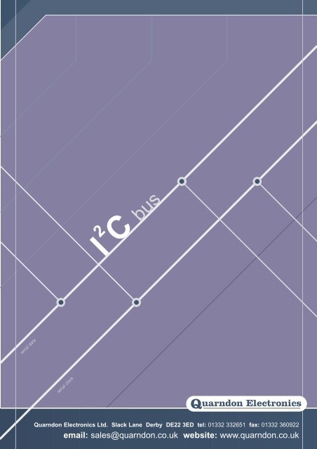
I 2 C bus<br />
serial data<br />
serial clock<br />
Quarndon Electronics<br />
Quarndon Electronics Ltd. Slack Lane Derby DE22 3ED tel: 01332 332651 fax: 01332 360922<br />
email: sales@quarndon.co.uk website: www.quarndon.co.uk
Contents<br />
3<br />
3<br />
4<br />
4<br />
5<br />
5<br />
6<br />
6<br />
7<br />
7<br />
8<br />
8<br />
9<br />
9<br />
Philips Semiconductor I2C Devices<br />
Typical I2C Product Characteristics<br />
I 2 C Bus Basics - Address and Data<br />
I 2 C General Purpose I/O Expanders<br />
I 2 C LED Drivers and Blinkers<br />
I 2 C Bus Extenders<br />
I 2 C Switches<br />
I 2 C Bus Repeater and Hub<br />
PCA9518, Expandable 5-Channel I2C Hub<br />
I 2 C Hot Swap Bus Buffer<br />
I 2 C Analog / Digital Converter<br />
Parallel Bus to I2C Bus Controller<br />
Multiplexed/Latched I2C EEPROMs<br />
I 2 C Multiplexers<br />
10<br />
part2<br />
11<br />
11<br />
12<br />
12<br />
13<br />
13<br />
14<br />
14<br />
15<br />
16<br />
16<br />
17<br />
18<br />
19<br />
19<br />
20<br />
20<br />
22<br />
22<br />
23<br />
Real-time Clock/calendar PCF8563<br />
Clock/calendar with Power Fail Detector PCF8573<br />
Clock/calendar with 240 x 8-bit RAM PCF8583<br />
Low power clock/calendar PCF8593<br />
8-bit / 16-bit I/O expander <strong>for</strong> I2C PCF8574, 8575<br />
I 2 C bus Controller PCF8584<br />
CMOS I2C EEPROMS PCF8582, 8594, 8598, 85116<br />
Low Voltage 258 x 8 - bit RAM PCF8570C<br />
8-bit A/D and D/A Converter PCF8591<br />
Universal LCD driver <strong>for</strong> low multiplex rates PCF8576C<br />
LCD Direct/Duplex Driver with I2C PCF8577C<br />
LCD row/column driver <strong>for</strong> dot matrix displays PCF8578, 8579<br />
Universal LCD driver <strong>for</strong> low multiplex rates PCF8566<br />
I 2 C Bus extender P82B715<br />
4 Digit LED-driver with I2C-Bus interface SAA1064<br />
CMDS 8-bit Microcontrollers P80C 552<br />
Philips P87C 524 / 528<br />
Philips P80C 652 / 587C652, 87C654<br />
PCompact 80C51 with I2C P87C 751<br />
Compact 80C51 with Analogue I/O P87C 752<br />
email sales@quarndon.co.uk | website www.quarndon.co.uk 2
Philips Semiconductor I 2 C Devices<br />
• TV Reception<br />
• Radio Reception<br />
• Audio Processing<br />
• Infrared Control<br />
• DTMF<br />
• LCD display control<br />
• LED display control<br />
• Clocks/ timers<br />
• General Purpose I/ O<br />
• Bus Extension/ Control<br />
• A/ D and D/ A Converter<br />
• RAM<br />
• EEPROM<br />
• Hardware Monitors<br />
• TV Reception<br />
• Radio Reception<br />
• Audio Processing<br />
• Infrared Control<br />
• DTMF<br />
• LCD display control<br />
• LED display control<br />
• Clocks/ timers<br />
• 8 bit Microprocessors<br />
• 16 bit Microprocessors<br />
I 2 C devices are broken down<br />
into 16 different categories<br />
Focus on display and timing<br />
categories<br />
www.semiconductors.<br />
philips.com/I 2 C<br />
Real Time Clock<br />
LCD Driver<br />
•<br />
Type of function in device<br />
Description<br />
0M4085 96 segment LCD driver 16<br />
PCF2103<br />
24 character LCD controller/driver<br />
2<br />
PCF2104<br />
48 character LCD controller/driver<br />
2<br />
PCF2105<br />
48 character LCD controller/driver<br />
2<br />
PCF2113<br />
24 character +120 icon LCD controller/driver<br />
2<br />
PCF2116<br />
48 character LCD controller/driver<br />
2<br />
PCF2119<br />
32 character LCD controller/driver<br />
2<br />
PCF8531<br />
34 x 128 graphic LCD controller/driver<br />
2<br />
PCF8533<br />
320 segment LCD driver<br />
16<br />
PCF8535<br />
(65 + icon row) x 133 graphic LCD controller/driver<br />
4<br />
PCF8548<br />
65 x 102 graphic LCD controller/driver<br />
2<br />
PCF8549<br />
65 x 102 graphic LCD controller/driver<br />
2<br />
PCF8558 • 40 x 101 graphic LCD controller/driver<br />
2<br />
PCF8563 • ultra low power real time clock/calendar<br />
1<br />
PCF8566 • 96 segment LCD driver<br />
16<br />
PCF8573 • real time clock/calendar with power fail detector<br />
4<br />
PCF8576C<br />
160 segment LCD driver<br />
16<br />
PCF8577C<br />
64 segment LCD driver<br />
16<br />
PCF8578<br />
384+ segment LCD driver<br />
2<br />
PCF8579 • 384+ segment LCD driver<br />
2<br />
PCF8583<br />
real time clock/calendar with 240 x 8 bit RAM<br />
2<br />
PCF8593 • low power real time clock/calendar<br />
1<br />
PCF8811<br />
80 x 128 graphic LCD controller/driver<br />
4<br />
PCF8813<br />
67 x 101 4 greyscale graphic LCD controller/driver<br />
4<br />
PCF8814<br />
80 x 96 graphic LCD controller/driver<br />
4<br />
PCF8820<br />
67 x 101 4 greyscale graphic LCD controller/driver<br />
4<br />
PCF8831<br />
160 x 128RGB 256 colour STN controller/driver chipset 4<br />
PCF8832<br />
160 x 128RGB 256 colour STN controller/driver chipset 4<br />
Addresses<br />
Interrupt (Out)<br />
Hardware reset<br />
1<br />
1<br />
1<br />
1.0<br />
1.8<br />
Vcc Range (V)<br />
2.5<br />
3.3<br />
5<br />
5V tolerant<br />
100<br />
Features<br />
FREQ(kHz)<br />
2<br />
• •<br />
•••••••• •<br />
• •••••••••• •<br />
•<br />
•<br />
• •<br />
• • •<br />
••••••••••••••• •<br />
8<br />
• •<br />
•<br />
16<br />
1.1<br />
• •<br />
•<br />
8<br />
8<br />
•<br />
1.5<br />
• •<br />
•• •<br />
1.5<br />
• • •••••••••••••••••••••••••• •<br />
•<br />
•<br />
•<br />
1.5<br />
• • • •<br />
•<br />
400<br />
3400<br />
TEMP<br />
40 to 85 ºC<br />
Pin count<br />
Bare die<br />
TCP<br />
Other<br />
Packages<br />
DIP<br />
VSO40<br />
LQFP100<br />
P<br />
P T<br />
VS040<br />
P<br />
T<br />
LQFP64/VS056<br />
LQFP64<br />
LQFP64/VS056<br />
P<br />
P<br />
SO (narrow)<br />
T<br />
T<br />
SO (wide)<br />
TSSOP<br />
Typical I 2 C product chart<br />
DP<br />
Typical I 2 C Product Characteristics<br />
• Frequency Range<br />
Typically 100 kHz operation with newer general purpose devices operating up to 400 kHz to<br />
support newer, higher frequency applications.<br />
• Operating Supply Voltage Range<br />
2.5 to 5.5 V or 2.7 to 5.5V with newer devices at 2.3 to 5.5V or 3.0 to 3.6V with 5V tolerance<br />
• Operates on both I 2 C and SMBus<br />
• Operating temperature range<br />
Typically -40 to +85 ºC with some 0 to +70 ºC or 0 to +120 ºC<br />
• Hardware address pins<br />
Typically three (A O, A 1, A 2) are provided to allow up to eight of the identical device on the<br />
same I 2 C bus but sometimes due to pin limitations there are fewer<br />
• Package Offerings<br />
Typically older devices in DIP, SO or SSOP. New devices will be offered only in SO and<br />
TSSOP and with future devices in TVSOP or MLP<br />
3<br />
Quarndon Electronics Ltd. | tel 01332 332651 | fax 01332 360922
I 2 C Bus Basics - Address and Data<br />
SCL<br />
I/O<br />
A/D<br />
D/A<br />
LCD<br />
RTC<br />
µcontroller<br />
µcontroller<br />
II<br />
SDA<br />
Each device is addressed<br />
individually by software with a<br />
unique address that can be<br />
modified by hardware pins<br />
1010A 1 A 2 A 3 R/W<br />
A0<br />
A1<br />
A2<br />
new<br />
function<br />
New devices or functions<br />
can be easily clipped on<br />
to an existing bus!<br />
Write data<br />
Master<br />
Slave<br />
S slave address W A data A data A P<br />
transmitter<br />
receiver<br />
Read data<br />
< n data bytes ><br />
S slave address R A data A data A P<br />
receiver<br />
transmitter<br />
< n data bytes > last data byte<br />
Data is transmitted at speeds of 100kHz, 400kHz or 3.4 MHz.<br />
S = Start condition<br />
A = Acknowledge<br />
P = Stop condition<br />
I 2 C General Purpose I/O Expanders<br />
• Used <strong>for</strong> general-purpose input and output<br />
(GPIO) extension from the I 2 C/SMBus.<br />
• Connect parallel I/O to the serial I 2 C/SMBus<br />
and provide expansion capability <strong>for</strong> te I/O<br />
controller Hub (South Bridge).<br />
• Four sets registers <strong>for</strong>:<br />
- Configuration (I or O)<br />
- Input (value)<br />
- Output (value)<br />
- Polarity (active high or low)<br />
• Devices have either Interrupt or Hardware Reset pin.<br />
• PCA9554, 8-bit I 2 C and SMBus I/O Port with Interrupt<br />
I 2 C Bus<br />
Interrupt Pin<br />
Reset Pin<br />
Input<br />
keypad or switch<br />
Output<br />
relay or enable pin or<br />
LED<br />
• PCA9554, 8-bit I 2 C and SMBus I/O Port with Interrupt<br />
• PCA9554A, 8-bit I 2 C and SMBus I/O Port with Interrupt<br />
• PCA9555, 16-bit I 2 C and SMBus I/O Port with Interrupt<br />
• PCA9556, Octal SMBus and I 2 C Registered Interface<br />
• PCA9557, Octal SMBus and I 2 C Registered Interface<br />
# of Outputs<br />
Reset and POR Interrupt and POR POR and 2K EEPROM Interrupt and POR and 2K EEPROM<br />
Quasi Output (20-25 ma sink and 100 uA source)<br />
8 -<br />
PCA9556/57<br />
PCA9556/57<br />
PCA9556/57<br />
16<br />
- PCF8575<br />
- -<br />
True Output (20-25 ma sink and 10 mA source)<br />
8<br />
16<br />
PCA9556/57<br />
-<br />
PCA9556/57A<br />
PCA9555<br />
PCA9558<br />
-<br />
-<br />
-<br />
email sales@quarndon.co.uk | website www.quarndon.co.uk 4
I 2 C LED Drivers and Blinkers<br />
• Used <strong>for</strong> general-purpose LED driving and blinking<br />
• Internal oscillator, no external components required.<br />
• Two user definable blink rates and duty cycles.<br />
• Single transmission to turn LEDs on, off, or blink at<br />
one of the two programmable blink rates.<br />
• I 2 C/SMBus not tied up by sending repeated<br />
transmissions to blink LEDs.<br />
• Hardware Reset pin.<br />
• High current open drain outputs.<br />
I 2 C Bus<br />
Reset Pin<br />
Oscillator<br />
Output<br />
LED<br />
Input<br />
LED<br />
• PCA9550, 2-Bit I 2 C/SMBus LED Driver and Blinker<br />
• PCA9551, 8-bit I 2 C/SMBus LED Driver and Blinker<br />
• PCA9552, 16-bit I 2 C/SMBus LED Driver and Blinker<br />
# of Outputs<br />
2<br />
8<br />
16<br />
Reset and POR<br />
PCA9550<br />
PCA9551<br />
PCA9552<br />
I 2 C Bus Extenders<br />
+V CC = 15V<br />
+V CC = 15V<br />
+5V 1k<br />
1k<br />
+5V<br />
SDA<br />
Tx<br />
Tx<br />
SI<br />
Rx<br />
* 15V Note: Schottky 15V *<br />
Rx<br />
diode or Zener clamps<br />
may be needed to limit<br />
spurious signals on<br />
1/2 P82B96 very long wiring<br />
1/2 P82B96<br />
*<br />
+V CC +V CC1<br />
KEY POINTS<br />
• High drive output are used to extend the reach of the I 2 C bus and<br />
exceed the 400 pF/system limit.<br />
• Typical distances - twisted wire (310’), Flat Ribbon Cable (1320’)<br />
• P82B96 has split high drive outputs which allows differential<br />
transmission and Opto-Electrical isolation of the I 2 C Bus<br />
I 2 C<br />
SDA<br />
+5V<br />
RxD<br />
(SDA)<br />
TxD<br />
(SDA)<br />
I 2 C<br />
SDA<br />
1/2 P82B96<br />
N.C.<br />
1<br />
8<br />
V CC<br />
Ex<br />
1<br />
8<br />
V CC<br />
L X<br />
S X<br />
GND<br />
2<br />
3<br />
4<br />
P82B715<br />
7<br />
6<br />
5<br />
L Y<br />
S Y<br />
N.C.<br />
Rx<br />
Tx<br />
GND<br />
2<br />
3<br />
4<br />
P82B96<br />
7<br />
6<br />
5<br />
S Y<br />
R Y<br />
Ty<br />
5<br />
Quarndon Electronics Ltd. | tel 01332 332651 | fax 01332 360922
I 2 C Switches<br />
I 2 C Bus<br />
OFF<br />
I 2 C Bus 0<br />
I 2 C Bus 1<br />
Reset<br />
Interrupt Out<br />
I 2 C<br />
Controller<br />
OFF<br />
Interrupt 0<br />
Interrupt 1<br />
FEATURES<br />
• Fan out main I 2 C/SMBus to multiple channels<br />
• Select off or individual downstream channels one at a<br />
time, all at once or in any combination.<br />
• I 2 C/SMBus commands used to select channel<br />
• Hardware Reset pin or POR opens all channels<br />
• Interrupt logic provides flag to master<br />
KEY POINTS<br />
• Switches allow the master to communicate to one<br />
channel or multiple downstream channels at a time but<br />
don’t isolate the bus capacitance<br />
• Other Applications include: sub-branch isolation and<br />
I 2 C/SMBus level shifting (1.8, 2.5, 3.3 or 5.0V)<br />
I 2 C Bus Repeater and Hub<br />
400<br />
pf<br />
SCL0<br />
SCA0<br />
PCA9515<br />
SCL1<br />
SCA1<br />
400<br />
pf<br />
Enable<br />
400<br />
pf<br />
400<br />
pf<br />
400<br />
pf<br />
SCLO<br />
SCAO<br />
SCL1<br />
SDA1<br />
E1<br />
SCL2<br />
SDA2<br />
GND<br />
1<br />
2<br />
3<br />
4<br />
5<br />
6<br />
7<br />
8<br />
PCA9516<br />
16<br />
15<br />
14<br />
13<br />
12<br />
11<br />
10<br />
9<br />
V CC<br />
E4<br />
SDA4<br />
SCL4<br />
E3<br />
SDA3<br />
SCL3<br />
E2<br />
400<br />
pf<br />
400<br />
pf<br />
I 2 C Bus Repeater<br />
5-Channel I 2 C Hub<br />
FEATURES<br />
• Bi-directional I 2 C drivers isolate the I 2 C bus<br />
capacitance to each segment.<br />
• Multi-master capable (e.g., repeater transparent to bus<br />
arbitration and contention protocol) with only one<br />
repeater delay between segments.<br />
• Segments can be individually isolated<br />
KEY POINTS<br />
• Accommodate more I 2 C devices or a longer bus length<br />
(i.e., up to 400 pF/segment)<br />
• Voltage Level Translation - 3.3V or 5V voltage<br />
levels allowed on the segment.<br />
• Only one hub or repeater is allowed in a I 2 C system<br />
email sales@quarndon.co.uk | website www.quarndon.co.uk 6
PCA9518, Expandable 5-Channel I 2 C Hub<br />
Interconnect<br />
Bus<br />
Enables<br />
9518<br />
9518 9518 9518 9518<br />
I 2 C/SMBus<br />
1 2 3 4<br />
5 6 7 8 9 10 11 12 13 14 15 16<br />
17 18 19 20<br />
• Similar to the PCA9516 but with four extra open drain signal pins that allow the internal device logic to be<br />
interconnected into an unlimited number of segments with only one repeater delay between any two segments.<br />
• The PCA9518, like the PCA9515/16, is transparent to bus arbitration and contention protocols in a multi-master<br />
environment and any master can talk to any other master on any segment.<br />
• The enable pins can be used to isolate four of the five segments per device. Place a pull up resistor on the<br />
unisolatable segment and leave it unused if there is a requirement to enable or disable the segment.<br />
I 2 C Hot Swap Bus Buffer<br />
Enable<br />
SCLOUT<br />
SCLIN<br />
GND<br />
VCC<br />
SDAOUT<br />
SDAIN<br />
READY<br />
PCA9511<br />
Heart Microprocessor<br />
Terminators<br />
Backplane Trace<br />
Connectors<br />
• Allows I/O card insertion into a live backplane without corruption of the data and clock busses.<br />
• Control circuitry prevents connected to the card until a stop bit or bus idle occurs on the backplane.<br />
• After connection, bi- directional buffering isolates capacitance and allowing 400 pF on either side.<br />
• PCA9511 can be used in series and more than one can be used in the same I 2 C system.<br />
• Rise time accelerator allows use of weaker DC pull- up currents while still meeting rise time requirements.<br />
• SDA and SCL lines are precharged to 1V, minimising current required to charge chip parasitic capacitance.<br />
• Incorporates a digital ENABLE input pin, which <strong>for</strong>ces the part into a low current mode when asserted low.<br />
• Open drain READY output pin indicates that the backplane and card sides are connected together.<br />
7<br />
Quarndon Electronics Ltd. | tel 01332 332651 | fax 01332 360922
I 2 C Analog / Digital Converter<br />
V REF<br />
Analog GND<br />
OSC Input switch<br />
Oscillator I/O<br />
Reset<br />
I 2 C Bus<br />
Analogue Input-Output<br />
Features<br />
• 4 channel<br />
• Internal oscillator<br />
• Hardware Reset pin and Power On Reset (POR)<br />
KEY POINTS<br />
• Converts signals from digital to analog and analog to digital<br />
• Two programmable thresholds above and below mean<br />
Voltage range Max I 2 C freq Resolution<br />
PCA8591 2.5 - 5.5V w/5V tolerance 100 kHz 100 kHz<br />
Parallel Bus to I 2 C Bus Controller<br />
I 2 C Bus<br />
I 2 C Interface<br />
Operation<br />
Control<br />
Control<br />
Bus Buffer<br />
Chip Enable<br />
Write Strobe<br />
Read Strobe<br />
Reset<br />
Address Inputs<br />
Interrupt Request<br />
Data (8-bits)<br />
Microcontroller<br />
FEATURES<br />
• Provides both master and slave functions.<br />
• Controls all the I 2 C bus specific sequences, protocol, arbitration and timing<br />
• Hardware Reset pin and Power On Reset (POR)<br />
KEY POINTS<br />
• Serves as an interface between most standard parallel-bus microcontrollers/ microprocessors and the serial I 2 C bus<br />
• Allows the parallel bus system to communicate with the I 2 C<br />
PCA8584<br />
PCA9564<br />
Voltage range Max I 2 C freq Clock source Parallel interface<br />
4.5 - 5.5V 90 kHz<br />
External<br />
Slow<br />
2.3 - 3.6V w/5V tolerance 360 kHz<br />
Internal<br />
Fast<br />
email sales@quarndon.co.uk | website www.quarndon.co.uk 8
Multiplexed/Latched I 2 C EEPROMs<br />
I 2 C Bus<br />
Hardware<br />
Input Pins<br />
EEPROM<br />
Mux<br />
Non MUX<br />
Output Pin<br />
Hardware<br />
Output Pins<br />
• Replacement <strong>for</strong> jumpers or dip switches.<br />
• I 2 C controlled integrated EEPROM and Multiplexer<br />
eliminates need to open equipment to modify<br />
jumpers/dip switches by hand.<br />
• Multiplex between the default values or the setting<br />
programmed from the I 2 C bus and stored in the onboard<br />
I 2 C EEPROM register.<br />
• The non-volatile I 2 C EEPROM register values stay<br />
resident even when the device is powered down.<br />
• PCA8550, 4-bit Multiplexed/I-bit<br />
Latched 5-bit EEPROM<br />
• PCA9559, 5-bit<br />
Multiplexed/I-bit Latched 6-bit EEPROM<br />
• PCA9560, Dual 5-bit<br />
Multiplexed/I-bit Latched EEPROM<br />
• PCA9561, Quad 6-bit Multiplexed EEPROM<br />
PCA8550<br />
PCA9559<br />
PCA9560<br />
PCA9561<br />
# of Non Volatile registers # of register bits # of hardware input bits # of Muxed output Non-muxed output<br />
1 5<br />
4 4 YES<br />
1<br />
2<br />
4<br />
6<br />
6<br />
6<br />
5<br />
5<br />
6<br />
5<br />
5<br />
6<br />
YES<br />
YES<br />
NO<br />
I 2 C Multiplexers<br />
I 2 C Bus 0<br />
I 2 C Bus 1<br />
I 2 C<br />
Controller<br />
Interrupt 0<br />
Interrupt 1<br />
FEATURES<br />
• Fan out main I 2 C/SMBus to multiple channels<br />
• Select off or individual downstream channel<br />
• I 2 C/SMBus commands used to select channel<br />
• Power On Reset (POR) opens all channels<br />
• Interrupt logic provides flag to master <strong>for</strong> system<br />
monitoring.<br />
KEY POINTS<br />
• Many specialised devices have only one I 2 C address and<br />
sometimes many are needed in the same system.<br />
• Multiplexers allow the master to communicate to one downstream<br />
channel at a time but don’t isolate the bus capacitance<br />
• Other Applications include sub-bach isolation.<br />
# of Channels POR Only Interrupt Logic and POR<br />
2 PCA9540<br />
PCA9542<br />
4<br />
-<br />
PCA9544<br />
9<br />
Quarndon Electronics Ltd. | tel 01332 332651 | fax 01332 360922
p a r t 2
Real-time Clock/calendar PCF8563<br />
CLK OUT<br />
DESCRIPTION<br />
The PCF8563 is a CMOS real-time clock/calendar<br />
optimized <strong>for</strong> low power consumption. A<br />
programmable clock output, interrupt output and<br />
voltage-low detector are also provided. The built-in<br />
word address register is incremented automatically<br />
after each written or read data byte.<br />
FEATURES<br />
• Provides year, month, day, weekday, hours, minutes<br />
and seconds based on 32.768 kHz quartz crystal<br />
• Century flag<br />
• Wide operating supply voltage range: 1.0 to 5.5V<br />
• Low back-up current; typical 0.25µA at VDD = 3.0V<br />
and Tamb = 25ºC<br />
• 400 kHz two-wire I 2 C-bus interface<br />
(at VDD = 1.8 to 5.5V)<br />
• Programmable clock output <strong>for</strong><br />
32.768 kHz, 1.24 Hz, 32 Hz 1 Hz<br />
• Alarm and timer functions<br />
• Integrated oscillator capacitor<br />
• Internal power-on reset<br />
OSCI<br />
OSCO<br />
INT<br />
VSS<br />
VSS<br />
SCL<br />
SDA<br />
Type number<br />
PCF8563P/F4<br />
PCF8563T/F4<br />
PCF8563TS/F4<br />
PCF8583<br />
Oscillator<br />
32.768 kHz<br />
Voltage<br />
Detector<br />
Oscillator<br />
Monitor<br />
I 2 C-BUS<br />
Interface<br />
Package<br />
DIP 8<br />
SO 8<br />
TSSOP 8<br />
POR<br />
Divider<br />
1:256<br />
or<br />
100 : 128<br />
Control<br />
logic<br />
Address<br />
FF register<br />
OSCI<br />
OSCO<br />
INT<br />
V SS<br />
1<br />
2<br />
3<br />
4<br />
control/status 1<br />
control/status 1<br />
second/VL<br />
minutes<br />
hours<br />
days<br />
weekdays<br />
months/century<br />
years<br />
minute alarm<br />
hour alarm<br />
day alarm<br />
weekday alarm<br />
clkout control<br />
timer control<br />
timer<br />
PCF8563P<br />
PCF8563T<br />
PCF8563TS<br />
8<br />
7<br />
6<br />
5<br />
0<br />
1<br />
2<br />
3<br />
4<br />
5<br />
6<br />
7<br />
8<br />
9<br />
A<br />
B<br />
C<br />
D<br />
E<br />
F<br />
V DD<br />
CLKOUT<br />
SCL<br />
SDA<br />
slave address<br />
1 0 1 0 0 0 A0 R/W<br />
Clock/calendar with Power Fail Detector PCF8573<br />
DESCRIPTION<br />
The PCF8573 is a low threshold,<br />
CMOS circuit that functions as a<br />
real time clock/calendar.<br />
A0<br />
A1<br />
1<br />
2<br />
16<br />
15<br />
V DD<br />
V SS1<br />
The IC incorporates an<br />
addressable time counter and an<br />
addressable alarm register <strong>for</strong><br />
minutes, hours, days and months.<br />
COMP<br />
SDA<br />
SCL<br />
EXTPF<br />
3<br />
4<br />
5<br />
6<br />
PCF8573P<br />
PCF8573T<br />
14<br />
13<br />
12<br />
11<br />
OSC0<br />
OSC1<br />
TEST<br />
FSET<br />
PFIN<br />
7<br />
10<br />
SEC<br />
FEATURES<br />
• Serial output I 2 C-bus<br />
• Alarm register <strong>for</strong> presetting<br />
a time <strong>for</strong> alarm or remote<br />
switching functions<br />
• On-chip power fail detector<br />
• Additional pulse outputs <strong>for</strong> seconds and minutes<br />
• Separate ground pin <strong>for</strong> the clock allows easy implementation<br />
of battery back-up during supply interruption<br />
• 1.2V nickel cadmium battery<br />
• Crystal oscillator control (32.768 kHz)<br />
• Low power consumption<br />
Type number<br />
PCF8573P<br />
PCF8573T<br />
slave address<br />
Package<br />
DIP 16<br />
SO 16<br />
V SS2<br />
8<br />
9<br />
MIN<br />
1 1 0<br />
1 0 A1 A0 R/W<br />
11<br />
Quarndon Electronics Ltd. | tel 01332 332651 | fax 01332 360922
Clock/calendar with 240 x 8-bit RAM PCF8583<br />
DESCRIPTION<br />
The PCF8583 is a clock/calendar circuit based on a<br />
256 x 8-bit static CMOS RAM. The built-in word<br />
address register is incremented automatically after<br />
each written or read data byte. Address pin AO is<br />
used <strong>for</strong> programming the hardware address, allowing<br />
the connection of two devices to the bus without<br />
additional hardware.The built-in 32.768 kHz oscillator<br />
circuit and the first 8 bytes of the RAM are used <strong>for</strong><br />
the clock/calendar and counter functions. The next 8<br />
bytes may be programmed as alarm registers or used<br />
as free RAM space. The remaining 240 bytes are free<br />
RAM locations.<br />
OSCI<br />
OSCO<br />
INT<br />
VSS<br />
VSS<br />
A0<br />
SCL<br />
SDA<br />
PCF8583<br />
Oscillator<br />
32.768 kHz<br />
Power-on<br />
reset<br />
I 2 C-BUS<br />
Interface<br />
Divider<br />
1:256<br />
or<br />
100 : 128<br />
Control<br />
logic<br />
Address<br />
FF register<br />
control/status<br />
hundredth of a second<br />
second<br />
minutes<br />
hours<br />
year/date<br />
weekdays/months<br />
timer<br />
alarm control<br />
alarm registers<br />
or RAM<br />
RAM<br />
(240 x 8)<br />
00<br />
01<br />
07<br />
08<br />
0F<br />
FF<br />
FEATURES<br />
• Clock operating supply voltage<br />
(0 to +70 ºC): 1.0 V to 6.0 V max. 50µA<br />
• 240 x 8-bit low-voltage RAM<br />
• Data retention voltage: 1.0 V to 6 V<br />
• Clock function with four year calendar<br />
• Universal timer with alarm and overflow indication<br />
• 24 or 12 hour <strong>for</strong>mat<br />
• 32.768 kHz or 50 Hz time base<br />
• Slave address: - READ: A1 or A3<br />
- WRITE: A0 or A2<br />
Type number<br />
PCF8583P/F5<br />
PCF8583T/F5<br />
Package<br />
DIP 8<br />
SOL 8<br />
slave address<br />
OSCI<br />
OSCO<br />
A0<br />
V SS<br />
1<br />
2<br />
3<br />
4<br />
PCF8583P<br />
PCF8583T<br />
8<br />
7<br />
6<br />
5<br />
V DD<br />
INT<br />
SCL<br />
SDA<br />
1 0 1<br />
0 0 0 A0 R/W<br />
Low power clock/calendar PCF8593<br />
DESCRIPTION<br />
The PCF8593 is a CMOS clock/calendar circuit,<br />
optimized <strong>for</strong> low power consumption. The built-in word<br />
address register is incremented automatically after<br />
each written or read data byte. The built-in 32.768 kHz<br />
oscillator circuit and the first 8 bytes of RAM are used<br />
<strong>for</strong> the clock/calendar and counter functions. The next<br />
8 bytes may be programmed as alarm registers or<br />
used as free RAM space.<br />
OSCI<br />
OSCO<br />
INT<br />
reset<br />
PCF8583<br />
Oscillator<br />
32.768 kHz<br />
reset<br />
Divider<br />
1:256<br />
or<br />
100 : 128<br />
Control<br />
logic<br />
control/status<br />
hundredth of a second<br />
second<br />
minutes<br />
hours<br />
year/date<br />
weekdays/months<br />
timer<br />
alarm control<br />
00<br />
01<br />
07<br />
08<br />
SCL<br />
SDA<br />
I 2 C-BUS<br />
Interface<br />
Address<br />
FF register<br />
alarm registers<br />
or RAM<br />
0F<br />
FEATURES<br />
• Operating supply voltage: 2.5 to 6.0 V<br />
• 8 bytes scratchpad RAM (when alarm not used)<br />
• Data retention voltage: 1.0 to 6.0 V<br />
• Operating current (fscl = 0 Hz, 32 kHz time base,<br />
VDD = 2.0 V): TYP. 1µA<br />
• Clock function with four year calendar<br />
• Universal timer with alarm and overflow indication<br />
• 24 or 12 hour <strong>for</strong>mat<br />
• 32.768 kHz or 50 Hz time base<br />
• Automatic word address incrementing<br />
• Slave address: - READ A3<br />
- WRITE A2<br />
Type number<br />
PCF8593P<br />
PCF8593T<br />
Package<br />
DIP 8<br />
SO 8<br />
slave address<br />
1 0 1 0 0 0 1 R/W<br />
OSCI<br />
OSCO<br />
RESET<br />
V SS<br />
1<br />
2<br />
3<br />
4<br />
PCF8593P<br />
PCF8593T<br />
8<br />
7<br />
6<br />
5<br />
V DD<br />
INT<br />
SCL<br />
SDA<br />
email sales@quarndon.co.uk | website www.quarndon.co.uk 12
8-bit / 16-bit I/O expander <strong>for</strong> I 2 C PCF8574, 8575<br />
DESCRIPTION<br />
The devices consist of an 8-bit/16-<br />
bit quasi-bidirectional port and an<br />
I 2 C-bus interface. The<br />
PCF8574/8575 have a low current<br />
consumption and include latched<br />
outputs with high current drive<br />
capability <strong>for</strong> directly driving LEDs.<br />
It also possesses an interrupt line<br />
(INT) which can be connected to<br />
the interrupt logic of the<br />
microcontroller.<br />
INT<br />
A0<br />
A1<br />
A2<br />
SCL<br />
SDA<br />
VDD<br />
VSS<br />
Input filter<br />
Power-on<br />
reset<br />
Interrupt logic<br />
I 2 C-BUS control<br />
PCF8574<br />
Shift<br />
Register<br />
Write pulse<br />
Read pulse<br />
LP Filter<br />
Input filter<br />
I/O<br />
Port<br />
4<br />
5<br />
6<br />
7<br />
8<br />
9<br />
10<br />
11<br />
P0<br />
P1<br />
P2<br />
P3<br />
P4<br />
P5<br />
P6<br />
P7<br />
A0<br />
A1<br />
A2<br />
P0<br />
P1<br />
P2<br />
P3<br />
V SS<br />
1<br />
2<br />
3<br />
4<br />
5<br />
6<br />
7<br />
8<br />
PCF8574<br />
PCF8574A<br />
16 V DD<br />
15 SDA<br />
14<br />
SCL<br />
13 INT<br />
12 P7<br />
11 P6<br />
10 P5<br />
9<br />
P4<br />
The PCF8574 and PCF8574A<br />
versions differ only in their slave<br />
address. The PCF8574A has an<br />
additional address bit, there<strong>for</strong>e 16<br />
devices can be addressed as<br />
opposed to 8.<br />
FEATURES<br />
• I 2 C to parallel port expander<br />
• Open-drain interrupt output<br />
• Remote I/O port <strong>for</strong> <strong>for</strong> the I 2 C-bus<br />
• Operating supply voltage 2.5 to 6V PCF8574<br />
• Low standby current consumption of<br />
10µA maximum<br />
slave address <strong>for</strong> 8574/8575<br />
0 1 0 0 A2 A1 A0 R/W<br />
slave address <strong>for</strong> 8574A<br />
0 1 1 1 A2 A1 A0 R/W<br />
PCF8575 is identical except that it has 16 I/O<br />
Part No.<br />
PCF8574AP<br />
PCF8574AT<br />
PCF8574P<br />
PCF8574T<br />
PCF8575CTS/F1<br />
PCF8575CT/F1<br />
Package<br />
DIP 16<br />
SOL 16<br />
DIP 16<br />
SOL 16<br />
SSOP 24<br />
SOL 24<br />
INT<br />
A1<br />
A2<br />
P00<br />
P01<br />
P02<br />
P03<br />
P04<br />
P05<br />
P06<br />
P07<br />
V SS<br />
1<br />
2<br />
3<br />
4<br />
5<br />
6<br />
7<br />
8<br />
9<br />
10<br />
11<br />
12<br />
PCF8575C<br />
24<br />
23<br />
22<br />
21<br />
20<br />
19<br />
18<br />
17<br />
16<br />
15<br />
14<br />
13<br />
V DD<br />
SDA<br />
SCL<br />
A0<br />
P17<br />
P16<br />
P15<br />
P14<br />
P13<br />
P12<br />
P11<br />
P10<br />
I 2 C bus Controller PCF8584<br />
DESCRIPTION<br />
The PCF8584 acts as an interface device between standard high-speed<br />
parallel buses and the serial I 2 C-bus. On the I 2 C-bus, it can act either as<br />
master or slave. Bidirectional data transfer between the I 2 C-bus and the<br />
parallel-bus microcontroller is carried out on a byte-wise basis, using either<br />
an interrupt or polled handshake. Interface to either 80XX-type (e.g. 8048,<br />
8051, Z80) or 68000-type buses is possible. Selection of bus type is<br />
automatically per<strong>for</strong>med.<br />
ADDRESS BUS<br />
A0<br />
ALE DECODER CS<br />
8048/8051<br />
DATA<br />
8048/8051<br />
RD<br />
FEATURES<br />
• Parallel-bus to I 2 C-bus protocol converter<br />
and interface<br />
• Compatible with most parallel-bus<br />
microcontrollers<br />
• Both master and slaver functions<br />
• Automatic detection and adaption to bus<br />
interface type<br />
• Programmable interrupt vector<br />
• Multi-master capability<br />
• I 2 C-bus monitor mode<br />
• Long-distance mode (4-wire)<br />
• Operating supply voltage 4.5 to 5.5 V<br />
CLK 1<br />
SDA 2<br />
SCL 3<br />
IACK 4<br />
INT 5<br />
A0 6<br />
DB0 7<br />
DB1 8<br />
DB2 9<br />
V SS 10<br />
PCF8584<br />
20<br />
19<br />
18<br />
17<br />
16<br />
15<br />
14<br />
13<br />
12<br />
11<br />
V DD<br />
RESET<br />
R/W<br />
CS<br />
RD<br />
DB7<br />
DB6<br />
DB5<br />
DB4<br />
DB3<br />
Part No.<br />
PCF8584P<br />
PCF8884T<br />
WR<br />
INT<br />
Package<br />
DIP 20<br />
SOL 20<br />
slave address<br />
0 1 1 1 A2 A1 A0 R/W<br />
13<br />
Quarndon Electronics Ltd. | tel 01332 332651 | fax 01332 360922
CMOS I 2 C EEPROMS PCF8582, 8594, 8598, 85116<br />
acknowledge<br />
from slave<br />
acknowledge<br />
from slave<br />
acknowledge<br />
from slave<br />
acknowledge<br />
from slave<br />
DESCRIPTION<br />
This family of CMOS I2C EEPRoms covers<br />
<strong>for</strong>mats 256x8,512x8, 1024x8 and 2048x8.<br />
Address select pins allow <strong>for</strong> a total of 2048 bytes<br />
of memory made up from 8 PCF8582, 4<br />
PCF8594, 2 PCF8598 on a single PCF85116. The<br />
PCF85116 has a second address field which<br />
allows selection of one of eight 256 byte blacks.<br />
When WP is taken high the upper half of a<br />
PCF8594, PCF8598 and the whole of PCF85116<br />
is write-protected.<br />
FEATURES<br />
• Max standby 10µA at 5.5V typical 4µA<br />
• Operational down to 2.7V<br />
• Single on 8 byte write modes<br />
(PCF85116 up to 32 bytes)<br />
• Sequential on Random Read<br />
• High Reliability by using redundant cells<br />
• Internal Write Times<br />
• Write Protect<br />
slave address<br />
1 0 1 0 A2 A1 A0 R/W<br />
S<br />
SLAVE ADDRESS 0 A WORD ADDRESS A S SLAVE ADDRESS<br />
R/W<br />
Type number<br />
PCF8582C-2P/03<br />
PCF8582C-2T/03<br />
PCF8594C-2P/02<br />
PCF8594C-2T/02<br />
PCF8598C-2P/02<br />
PCF8598C-2T/02<br />
PCF85116-3P/01<br />
PCF85116-3T/01<br />
at this moment master<br />
transmitter becomes master<br />
receiver and EEPROM slave<br />
receiver becomes slave<br />
transmitter<br />
Master reads PCF85xxC-2 slave after setting word<br />
address (write word address; read data)<br />
Package<br />
DIP 8<br />
SO 8<br />
DIP 8<br />
SO 8<br />
DIP 8<br />
SOL 8<br />
DIP 8<br />
SO 8<br />
Format<br />
256x8<br />
256x8<br />
512x8<br />
512x8<br />
1024x8<br />
1024x8<br />
2048x8<br />
2048x8<br />
1 A<br />
R/W<br />
n bytes<br />
auto increment word address<br />
no acknowledge<br />
from slave<br />
DATA 1 P<br />
n bytes<br />
DATA<br />
auto increment word address<br />
Max Current<br />
2.0µA<br />
2.0µA<br />
2.5µA<br />
2.5µA<br />
4.0µA<br />
4.0µA<br />
1.0µA<br />
1.0µA<br />
A<br />
A0<br />
1<br />
8<br />
V DD<br />
WP<br />
1<br />
8<br />
V DD<br />
WP<br />
1<br />
8<br />
V DD<br />
n.c.<br />
1<br />
8<br />
V DD<br />
A1<br />
A2<br />
2<br />
3<br />
PCF8582C-2<br />
7<br />
6<br />
PTC<br />
SCL<br />
A1<br />
A2<br />
2<br />
3<br />
PCF8594C-2<br />
7<br />
6<br />
PTC<br />
SCL<br />
n.c.<br />
A2<br />
2<br />
3<br />
PCF8598C-2<br />
7<br />
6<br />
PTC<br />
SCL<br />
n.c.<br />
n.c.<br />
2<br />
3<br />
PCF85116-3<br />
7<br />
6<br />
WP<br />
SCL<br />
V SS<br />
4<br />
5<br />
SDA<br />
V SS<br />
4<br />
5<br />
SDA<br />
V SS<br />
4<br />
5<br />
SDA<br />
V SS<br />
4<br />
5<br />
SDA<br />
Low Voltage 258 x 8 - bit RAM PCF8570C<br />
VDD<br />
DESCRIPTION<br />
The PCF85700C is ideal <strong>for</strong> applications requiring<br />
extremely low-current and low-voltage RAM retention,<br />
such as battery or capacitor - backed. See diagram <strong>for</strong> a<br />
typical multiple PCF8570C application.<br />
0<br />
A0<br />
0<br />
A1<br />
0<br />
A2<br />
TEST<br />
VDD<br />
PCF8570C<br />
‘1010’<br />
SCL<br />
SDA<br />
VSS<br />
SDA<br />
Master<br />
transmitter/<br />
SCL receiver<br />
FEATURES<br />
• Operating supply voltage 2.5<br />
to 6.0 V<br />
• Low data retention voltage;<br />
minimum 1.0 V<br />
• Low standby current;<br />
maximum 15 µA<br />
• Power-saving mode; typical<br />
50 nA<br />
• Serial input/output bus<br />
(I 2 C-bus)<br />
• Address by 3 hardware<br />
address pins<br />
• Automatic word address<br />
incrementing<br />
A0<br />
A1<br />
A2<br />
V SS<br />
1<br />
2<br />
3<br />
4<br />
Type number<br />
PCF8570P/F5<br />
PCF8570T/F5<br />
8570C<br />
8<br />
7<br />
6<br />
5<br />
V DD<br />
TEST<br />
SCL<br />
SDA<br />
Package<br />
DIP 8<br />
SOL 8<br />
slave address<br />
1 0 1 0 A2 A1 A0 R/W<br />
VDD<br />
1<br />
A0<br />
0<br />
A1<br />
0<br />
1<br />
A0<br />
1<br />
A1<br />
1<br />
A2<br />
TEST<br />
A2<br />
TEST<br />
VDD<br />
PCF8570C<br />
‘1010’<br />
VDD<br />
PCF8570C<br />
‘1010’<br />
SCL<br />
SDA<br />
VSS<br />
SCL<br />
SDA<br />
VSS<br />
SDA SCL<br />
(I 2 C-bus)<br />
up to 8 PCF8570C<br />
V DD<br />
R: pull-up resistor<br />
R R<br />
t r<br />
R =<br />
C BUS<br />
email sales@quarndon.co.uk | website www.quarndon.co.uk 14
8-bit A/D and D/A Converter PCF8591<br />
DESCRIPTION<br />
The PCF8591 is a low power 8-bit CMOS data<br />
acquisition device with four analog inputs, one<br />
analog output. Three address pins A), A1 and A2<br />
are used <strong>for</strong> programming the hardware address,<br />
allowing the use of up to eight devices.<br />
The functions of the device include analog input<br />
multiplexing, on-chip track and hold function, 8-bit<br />
analog-to-digital conversion and an 8-bit digital-toanalog<br />
conversion. The maximum conversion rate is<br />
given by the maximum speed of the I 2 C-bus.<br />
SCL<br />
SDA<br />
A0<br />
A1<br />
A2<br />
EXT<br />
VDD<br />
VSS<br />
OSC<br />
I 2 C BUS<br />
Interface<br />
Analogue<br />
multi-plexer<br />
Oscillator<br />
Status<br />
register<br />
Control logic<br />
Dac data<br />
register<br />
ADC data<br />
register<br />
AIN0<br />
AIN1<br />
AIN2<br />
AIN3<br />
Analogue<br />
multi-plexer<br />
S/H<br />
+<br />
comparator<br />
-<br />
Successive approximation<br />
register/logic<br />
FEATURES<br />
• Single power supply<br />
• Operating supply voltage 2.5 V to 6 V<br />
• Low standby current<br />
• Serial input/output via I 2 C-bus<br />
• Address by 3 hardware address pins<br />
• Sampling rate given by I 2 C-bus speed<br />
• 4 analog inputs programmable as single-ended or<br />
differential inputs<br />
• Auto-incremented channel selection<br />
• Analog voltage range from VSS to VDD<br />
• On-chip track and hold circuit<br />
• 8-bit successive approximation A/D conversion<br />
• Multiplying DAC with one analog<br />
AOUT<br />
S/H<br />
DAC<br />
VREF<br />
AGND<br />
AIN0<br />
1<br />
16<br />
V DD<br />
AIN1<br />
2<br />
15<br />
AOUT<br />
AIN2<br />
3<br />
PCF8591<br />
14<br />
VREF<br />
AIN3<br />
4<br />
13<br />
AGND<br />
A0<br />
5<br />
12<br />
EXT<br />
A1<br />
6<br />
11<br />
OSC<br />
A2<br />
7<br />
10<br />
SCL<br />
V SS<br />
8<br />
9<br />
SDA<br />
Type number<br />
PCA8591P<br />
PCA8591T<br />
Package<br />
DIP 16<br />
SO16<br />
slave address<br />
1 0 0<br />
1 A2 A1 A0 R/W<br />
15<br />
Quarndon Electronics Ltd. | tel 01332 332651 | fax 01332 360922
Universal LCD driver <strong>for</strong> low multiplex rates PCF8576C<br />
SDA<br />
1<br />
56<br />
S39<br />
DESCRIPTION<br />
The PCF8576C is a versatile peripheral device designed to interface to any microprocessor /<br />
microcontroller to a wide variety of LCDs. It can directly drive any static or multiplexed LCD<br />
containing up to four backplanes and up to 40 segments. The display configurations possible with<br />
the PCF8576C depend on the number of active backplane outputs required; a selection of<br />
display configurations is given in Table 1.<br />
SCL<br />
SYNC<br />
CLK<br />
V DD<br />
OSC<br />
A0<br />
A1<br />
2<br />
3<br />
4<br />
5<br />
6<br />
7<br />
8<br />
55<br />
54<br />
53<br />
52<br />
51<br />
50<br />
49<br />
S38<br />
S37<br />
S36<br />
S35<br />
S34<br />
S33<br />
S32<br />
A2<br />
9<br />
48<br />
S31<br />
SA0<br />
10<br />
VS056<br />
47<br />
S30<br />
FEATURES<br />
• Selectable backplane drive configuration: static or 2, 3,or 4 backplane multiplexing<br />
• Selectable display bias configuration: static, 1/2 or 1/3<br />
• Internal LCD bias generation with voltage-follower buffers<br />
• 40 segment drives: up to twelve 8-segment numeric characters; up to six 15-segment alphanumeric<br />
characters; or any graphics of up to 160 elements<br />
• Versatile blinking modes<br />
• Low power consumption<br />
V SS<br />
11<br />
V LCD 12<br />
BP0 13<br />
BP2 14<br />
BP1 15<br />
BP3 16<br />
S0 17<br />
S1 18<br />
S2 19<br />
46<br />
45<br />
44<br />
43<br />
42<br />
41<br />
40<br />
39<br />
38<br />
S29<br />
S28<br />
S27<br />
S26<br />
S25<br />
S24<br />
S23<br />
S22<br />
S21<br />
S3<br />
20<br />
37<br />
S20<br />
VDD<br />
VDD<br />
VLCD<br />
S4<br />
21<br />
36<br />
S19<br />
Type number<br />
PCF8576CT/F1<br />
PCF8576CH/F1<br />
Package<br />
VS056<br />
LQFP64<br />
Host microprocessor/<br />
microcontroller<br />
SDA<br />
SCL<br />
OSC<br />
1<br />
2<br />
3<br />
7<br />
5 12<br />
PCF8576CT<br />
8 9 10 11<br />
A0 A1 A2 SA0 VSS<br />
40 segment drives<br />
4 backplanes<br />
LCD panel<br />
(up to 160<br />
elements)<br />
S5<br />
S6<br />
S7<br />
S8<br />
22<br />
23<br />
24<br />
25<br />
35<br />
34<br />
33<br />
32<br />
S18<br />
S17<br />
S16<br />
S15<br />
VSS<br />
S9<br />
26<br />
31<br />
S14<br />
slave address<br />
0 1 1 1 0 0 A0 R/W<br />
S10<br />
S11<br />
27<br />
28<br />
30 S13<br />
29 S12<br />
LCD Direct/Duplex Driver with I 2 C PCF8577C<br />
DESCRIPTION<br />
The PCF8577C is a single chip, CMOS circuit, It is designed to drive liquid crystal displays<br />
with up to 32 segments directly, or 64 segments in a duplex configuration.<br />
S32<br />
S31<br />
S30<br />
1<br />
2<br />
3<br />
40<br />
39<br />
38<br />
SDA<br />
SCL<br />
V SS<br />
S29<br />
4<br />
37<br />
A0/OSC<br />
FEATURES<br />
• Direct/duplex drive modes with up to 32/64 LCD-segment drive capability per device<br />
• Auto-incremented loading across device subaddress boundaries<br />
• Operating supply voltage: 2.5 to 6 V<br />
• Low power consumption<br />
• Single-pin built-in oscillator<br />
• Display memory switching in direct drive mode<br />
• Power-on reset blanks display<br />
Type number<br />
PCF8577CP<br />
PCF8577CT<br />
Package<br />
DIP40<br />
VSO40<br />
S28<br />
S27<br />
S26<br />
S25<br />
S24<br />
S23<br />
5<br />
6<br />
7<br />
8<br />
9<br />
10<br />
PCF8577C<br />
36<br />
35<br />
34<br />
33<br />
32<br />
31<br />
A1<br />
V DD<br />
A2/BP2<br />
BP1<br />
S1<br />
S2<br />
S22<br />
11<br />
30<br />
S3<br />
SCL<br />
SDA<br />
39<br />
40<br />
Input<br />
filters<br />
I 2 C - Bus<br />
controller<br />
Segment byte registers<br />
and multiplex logic<br />
Backplane<br />
and<br />
segment<br />
driver<br />
1<br />
32<br />
33<br />
S32<br />
S1<br />
BP1<br />
S21<br />
S20<br />
S19<br />
S18<br />
12<br />
13<br />
14<br />
15<br />
29<br />
28<br />
27<br />
26<br />
S4<br />
S5<br />
S6<br />
S7<br />
VDD<br />
35<br />
34<br />
36<br />
37<br />
A2/BP2<br />
A1<br />
A0/OSC<br />
S17<br />
S16<br />
16<br />
17<br />
25<br />
24<br />
S8<br />
S9<br />
VSS<br />
38<br />
Power on reset<br />
PCF8577C<br />
Control register<br />
and comparator<br />
Oscillator and<br />
divider<br />
slave address<br />
0 1 1 1 0 1 0 R/W<br />
S15<br />
S14<br />
S13<br />
18<br />
19<br />
20<br />
23<br />
22<br />
21<br />
S10<br />
S11<br />
S12<br />
email sales@quarndon.co.uk | website www.quarndon.co.uk 16
LCD row/column driver <strong>for</strong> dot matrix displays PCF8578, 8579<br />
DESCRIPTION<br />
The PCF8578 is a low power<br />
CMOS LCD row/column driver,<br />
designed to drive dot matrix<br />
graphic displays at multiplex<br />
rates of 1 : 8, 1 : 16, 1 : 24 or 1 :<br />
32. The device has 40 outputs,<br />
of which 24 are programmable,<br />
configurable as 32 /8 , 24 /16 ,<br />
16 /24 or 8 /32 rows/columns.<br />
The PCF8578 can function as a<br />
stand-alone LCD controller/driver<br />
<strong>for</strong> use in small systems, or <strong>for</strong><br />
larger systems can be used in<br />
conjunction with up to 32<br />
PCF8579s <strong>for</strong> which it has been<br />
optimized. Together these two<br />
devices <strong>for</strong>m a general purpose<br />
LCD dot matrix driver chip set,<br />
capable of driving displays of up<br />
to 40960 dots.<br />
V DD<br />
R1<br />
C<br />
V 2<br />
HOST<br />
MICROCONTROLLER<br />
SCL<br />
SDA<br />
V SS<br />
C<br />
C<br />
C<br />
C<br />
R2<br />
R3<br />
R2<br />
R1<br />
V LCD<br />
R OSC<br />
V DD<br />
V 3<br />
V 4 PCF8578<br />
V 5<br />
V LCD<br />
V SS<br />
OSC<br />
n<br />
rows<br />
SA0<br />
SDA SCL CLK SYNC<br />
40 n<br />
columns<br />
V DD V DD<br />
V LCD<br />
V LCD<br />
subaddress 1<br />
V SS V SS<br />
V SS / V DD<br />
V SS / V DD<br />
V SS / V DD<br />
LCD DISPLAY<br />
SA0<br />
SDA<br />
SCL<br />
40<br />
columns<br />
A0<br />
A1<br />
PCF8579<br />
A2<br />
A3<br />
CLK SYNC V 4 V 3<br />
FEATURES<br />
• Stand-alone or may be used<br />
with up 32 PCF857s (40960<br />
dots possible)<br />
• 40 driver outputs, configurable<br />
as 32/8, 24/16, 16/24 or 8/32<br />
row/columns<br />
• Selectable multiplex rates;<br />
1 : 8, 1 : 16, 1 : 24 or 1 : 32<br />
• Provides display<br />
synchronisation <strong>for</strong> PCF8579<br />
• On-chip oscillator, requires<br />
only 1 external resistor<br />
• Power-on reset black display<br />
th<br />
R5 1<br />
R4 2<br />
R3 3<br />
R2 4<br />
R1 5<br />
R0 6<br />
SDA 7<br />
SCL 8<br />
SYNC 9<br />
CLK 10<br />
V SS 11<br />
TEST 12<br />
SA0 13<br />
n.c. 14<br />
n.c. 15<br />
OSC 16<br />
n.c. 17<br />
64 R6<br />
n.c. 18<br />
63 R7<br />
n.c. 19<br />
62 R8/C8<br />
V DD 20<br />
61 R9/C9<br />
V 2 21<br />
60 R10/C10<br />
22<br />
59 R11/C11<br />
V 3<br />
58 R12/C12<br />
57 R13/C13<br />
56 R14/C14<br />
55 R15/C15<br />
54 R16/C16<br />
53 R17/C17<br />
PCF8578<br />
LQFP64<br />
V 4 23<br />
V 5 24<br />
V LCD 25<br />
n.c. 26<br />
n.c. 27<br />
n.c. 28<br />
C39 29<br />
52 R18/C18<br />
C38 30<br />
51 R19/C19<br />
C37 31<br />
50 R20/C20<br />
C36 32<br />
49 R21/C21<br />
48 R22/C22<br />
47 n.c.<br />
46 R23/C23<br />
45 R24/C24<br />
44 R25/C25<br />
43 R26/C26<br />
42 R27/C27<br />
41 R28/C28<br />
40 R29/C29<br />
39 R30/C30<br />
38 R31/C31<br />
37 C32<br />
36 n.c.<br />
35 C33<br />
34 C34<br />
33 C35<br />
MBH588<br />
SDA<br />
SCL<br />
SYNC<br />
CLK<br />
V<br />
SS<br />
TEST<br />
SA0<br />
OSC<br />
V DD<br />
V 2<br />
V 3<br />
V 4<br />
V 5<br />
V LCD<br />
n.c.<br />
1<br />
2<br />
3<br />
4<br />
5<br />
6<br />
7<br />
8<br />
9<br />
10<br />
11<br />
12<br />
56<br />
55<br />
54<br />
53<br />
52<br />
51<br />
50<br />
49<br />
48<br />
47<br />
46<br />
45<br />
13 44<br />
14<br />
43<br />
PCF8578<br />
15<br />
42<br />
R0<br />
R1<br />
R2<br />
R3<br />
R4<br />
R5<br />
R6<br />
R7<br />
R8/C8<br />
R9/C9<br />
R10/C10<br />
R11/C11<br />
R12/C12<br />
R13/C13<br />
R14/C14<br />
SDA<br />
SCL<br />
SYNC<br />
CLK<br />
V<br />
SS<br />
TEST<br />
SA0<br />
A3<br />
A2<br />
A1<br />
A0<br />
1<br />
2<br />
3<br />
4<br />
5<br />
6<br />
7<br />
8<br />
9<br />
10<br />
11<br />
56<br />
55<br />
54<br />
53<br />
52<br />
51<br />
50<br />
49<br />
48<br />
47<br />
46<br />
V DD 12<br />
45<br />
n.c. 13 44<br />
V 3 14<br />
43<br />
PCF8579<br />
V 4 15<br />
42<br />
C0<br />
C1<br />
C2<br />
C3<br />
C4<br />
C5<br />
C6<br />
C7<br />
C8<br />
C9<br />
C10<br />
C11<br />
C12<br />
C13<br />
C14<br />
agewidth<br />
C6<br />
C7<br />
C8<br />
C9<br />
C10<br />
C11<br />
C12<br />
C13<br />
C14<br />
C15<br />
C16<br />
C17<br />
C18<br />
C19<br />
C20<br />
C21<br />
n.c. 16<br />
41<br />
R15/C15<br />
V LCD 16<br />
41<br />
C15<br />
C5 1<br />
C4 2<br />
64<br />
63<br />
62<br />
61<br />
60<br />
59<br />
58<br />
57<br />
56<br />
55<br />
54<br />
53<br />
52<br />
51<br />
50<br />
49<br />
48 C22<br />
47 C23<br />
C39<br />
C38<br />
17<br />
18<br />
40<br />
39<br />
R16/C16<br />
R17/C17<br />
C39<br />
C38<br />
17<br />
18<br />
40<br />
39<br />
C16<br />
C17<br />
Type number<br />
PCF8578T<br />
PCF8578H<br />
PCF8579T<br />
PCF8579H<br />
Package<br />
VS056<br />
LQFP64<br />
VS056<br />
LQFP64<br />
C3 3<br />
C2 4<br />
C1 5<br />
C0 6<br />
SDA 7<br />
SCL 8<br />
SYNC 9<br />
CLK 10<br />
V SS 11<br />
TEST 12<br />
SA0 13<br />
A3 14<br />
n.c. 15<br />
LQFP64<br />
PCF8579<br />
46 C24<br />
45 C25<br />
44 C26<br />
43 C27<br />
42 C28<br />
41 C29<br />
40 C30<br />
39 C31<br />
38 C32<br />
37 C33<br />
36 C34<br />
35 C35<br />
34 n.c.<br />
C37<br />
C36<br />
C35<br />
C34<br />
C33<br />
C32<br />
R31/C31<br />
R30/C30<br />
19<br />
20<br />
21<br />
22<br />
23<br />
24<br />
25<br />
26<br />
38<br />
37<br />
36<br />
35<br />
34<br />
33<br />
32<br />
31<br />
R18/C18<br />
R19/C19<br />
R20/C20<br />
R21/C21<br />
R22/C22<br />
R23/C23<br />
R24/C24<br />
R25/C25<br />
C37<br />
C36<br />
C35<br />
C34<br />
C33<br />
C32<br />
C31<br />
C30<br />
19<br />
20<br />
21<br />
22<br />
23<br />
24<br />
25<br />
26<br />
38<br />
37<br />
36<br />
35<br />
34<br />
33<br />
32<br />
31<br />
C18<br />
C19<br />
C20<br />
C21<br />
C22<br />
C23<br />
C24<br />
C25<br />
A2 16<br />
33 C36<br />
R29/C29<br />
27<br />
30<br />
R26/C26<br />
C29<br />
27<br />
30<br />
C26<br />
17<br />
A1<br />
18<br />
A0<br />
19<br />
n.c.<br />
20<br />
V DD<br />
21<br />
n.c.<br />
22<br />
V 3<br />
23<br />
V 4<br />
24<br />
V LCD<br />
25<br />
n.c.<br />
26<br />
n.c.<br />
27<br />
n.c.<br />
28<br />
n.c.<br />
29<br />
n.c.<br />
30<br />
C39<br />
31<br />
C38<br />
32<br />
C37<br />
MBH590<br />
R28/C28<br />
28<br />
MSA839<br />
29<br />
R27/C27<br />
C28<br />
28<br />
MSA918<br />
29<br />
C27<br />
slave address<br />
0 1 1<br />
1 1 0 A0 R/W<br />
17<br />
Quarndon Electronics Ltd. | tel 01332 332651 | fax 01332 360922
Universal LCD driver <strong>for</strong> low multiplex rates PCF8566<br />
DESCRIPTION<br />
The PCF8566 is a peripheral device which interfaces to almost<br />
any Liquid Crystal Display (LCD) having low multiplex rates. It<br />
generates the drive signals <strong>for</strong> any static or multiplexed LCD<br />
containing up to four backplanes and up to 24 segments and can<br />
easily be cascaded <strong>for</strong> larger LCD applications.<br />
S32<br />
SCL<br />
SYNC<br />
CLK<br />
V DD<br />
1<br />
2<br />
3<br />
4<br />
5<br />
PCF8566<br />
40<br />
39<br />
38<br />
37<br />
36<br />
S23<br />
S22<br />
S21<br />
S20<br />
S19<br />
OSC<br />
6<br />
35<br />
S18<br />
FEATURES<br />
• Single-chip LCD controller/driver<br />
• Selectable backplane drive configuration: static or 2, 3,or 4 back<br />
plane multiplexing<br />
• Selectable display bias configuration: static, 1/2 or 1/3<br />
• Internal LCD bias generation with voltage-follower buffers<br />
• 24 segment drives: up to twelve 8-segment numeric characters; uo<br />
to six 15-segment alphanumeric characters; or any graphics of up to<br />
96 elements<br />
• Versatile blinking modes<br />
• 2.5 to 6V power supply range<br />
• Low power consumption<br />
• May be cascaded <strong>for</strong> large LCD applications<br />
(up to 1536 segments possible)<br />
A0<br />
A1<br />
A2<br />
SA0<br />
V SS<br />
V LCD<br />
BP0<br />
BP2<br />
BP1<br />
BP3<br />
7<br />
8<br />
9<br />
10<br />
11<br />
12<br />
13<br />
14<br />
15<br />
16<br />
34<br />
33<br />
32<br />
31<br />
30<br />
29<br />
28<br />
27<br />
26<br />
25<br />
S17<br />
S16<br />
S15<br />
S14<br />
S13<br />
S12<br />
S11<br />
S10<br />
S9<br />
S8<br />
S0<br />
17<br />
24<br />
S7<br />
Type number<br />
PCF8566P<br />
PCF8566T<br />
Package<br />
DIP 40<br />
SO 40<br />
slave address<br />
0 1 1 1 1 1 A0 R/W<br />
S1<br />
S2<br />
S3<br />
18<br />
19<br />
20<br />
23<br />
22<br />
21<br />
S6<br />
S5<br />
S4<br />
h<br />
BP0 BP2 BP1 BP3<br />
S0 to S23<br />
V DD<br />
5<br />
R<br />
13<br />
14<br />
15<br />
BACKPLANE<br />
OUTPUTS<br />
16<br />
17 to 40<br />
DISPLAY SEGMENT OUTPUTS<br />
R<br />
LCD<br />
VOLTAGE<br />
SELECTOR<br />
DISPLAY LATCH<br />
V LCD<br />
12<br />
R<br />
LCD BIAS<br />
GENERATOR<br />
SHIFT REGISTER<br />
CLK<br />
SYNC<br />
OSC<br />
V SS<br />
4<br />
3<br />
6<br />
11<br />
TIMING<br />
OSCILLATOR<br />
BLINKER<br />
POWER-<br />
ON<br />
RESET<br />
PCF8566<br />
DISPLAY<br />
CONTROLLER<br />
COMMAND<br />
DECODER<br />
INPUT<br />
BANK<br />
SELECTOR<br />
DISPLAY<br />
RAM<br />
24 × 4 BITS<br />
DATA<br />
POINTER<br />
OUTPUT<br />
BANK<br />
SELECTOR<br />
SCL<br />
SDA<br />
2<br />
1<br />
INPUT<br />
FILTERS<br />
2<br />
I C-BUS<br />
CONTROLLER<br />
SUB-<br />
ADDRESS<br />
COUNTER<br />
10<br />
7<br />
8<br />
9<br />
SA0<br />
A0<br />
A1<br />
A2<br />
email sales@quarndon.co.uk | website www.quarndon.co.uk 18
I 2 C Bus extender P82B715<br />
DESCRIPTION<br />
The 82B715 is a bipolar integrated<br />
circuit intended <strong>for</strong> application in<br />
I 2 C bus systems.<br />
While retaining all the operating<br />
modes and features of the I 2 C<br />
system it permits extension of the<br />
practical separation distance<br />
between components on the I 2 C<br />
bus by buffering both the data<br />
(SDA) and the clock (SCL) lines.<br />
SDA<br />
SCL<br />
STANDARD<br />
I 2 C<br />
INTERFACE<br />
82B715<br />
1/2<br />
1/2<br />
V CC<br />
V CC<br />
BUFFERED<br />
INTERFACE<br />
LONG<br />
CABLE<br />
LDA<br />
LCL<br />
BUFFERED<br />
INTERFACE<br />
82B715<br />
1/2<br />
1/2<br />
SDA<br />
SCL<br />
STANDARD<br />
I 2 C<br />
INTERFACE<br />
I 2 C<br />
DEVICE<br />
The I 2 C bus capacitance limit of<br />
400pF restricts practical<br />
communication distances to a few<br />
meters. Using one 82B715 at each<br />
end of longer cables reduces the<br />
cable loading capacitance on the<br />
I 2 C<br />
SDA<br />
SCL<br />
82B715<br />
V CC<br />
BUFFER<br />
BUFFER<br />
LDA<br />
LCL<br />
N.C.<br />
L X<br />
S X<br />
1<br />
2<br />
3<br />
82B715<br />
8<br />
7<br />
6<br />
V CC<br />
L Y<br />
S Y<br />
GND<br />
4<br />
5<br />
N.C.<br />
FEATURES<br />
• Dual, bi-directional, unity voltage gain buffet<br />
• I 2 C bus compatible<br />
• Logic signal levels may include both supply and ground<br />
• X10 impedance trans<strong>for</strong>mation<br />
• Wide supply voltage range<br />
GND<br />
Type number<br />
P82B715N<br />
P82B715D<br />
Package<br />
DIP 40<br />
SO 40<br />
4 Digit LED-driver with I 2 C-Bus interface SAA1064<br />
DESCRIPTION<br />
The LED-driver is a bipolar integrated circuit<br />
made in an I 2 L compatible 18 volts process. The<br />
circuit is especially designed to drive four 7-<br />
segment LED displays with decimal point by<br />
means of multiplexing between two pairs of<br />
digits. It features an I 2 C-Bus slave transceiver<br />
interface with the possibility to program four<br />
different SLAVE ADDRESSES, a POWER<br />
RESET flag, 16 current sink OUTPUTS,<br />
controllable by software up to 21mA, two<br />
multiplex drive outputs <strong>for</strong> common anode<br />
segments, an on-chip multiplex drive outputs <strong>for</strong><br />
common anode segments, an on-chip multiplex<br />
oscillator, control bits to select static, dynamic<br />
and blank mode, and one bit <strong>for</strong> segment test.<br />
Part No.<br />
SAA1064<br />
SAA1064T<br />
Package<br />
DIP 24<br />
SOL 24<br />
slave address<br />
0 1 1<br />
1 0 A1 A0 R/W<br />
19<br />
Quarndon Electronics Ltd. | tel 01332 332651 | fax 01332 360922
CMDS 8-bit Microcontrollers P80C 552<br />
DESCRIPTION<br />
The PCF8577C is a single chip,<br />
silicon gate CMOS circuit, It is<br />
designed to drive liquid crystal<br />
displays with up to 32 segments<br />
directly, or 64 segments in a<br />
duplex configuration.<br />
The two-line I 2 C-bus interface<br />
substantially reduces wiring<br />
overheads in remote display<br />
applications. I 2 C-bus traffic is<br />
minimised in multiple IC<br />
applications by automatic<br />
address incrementing, hardware<br />
subaddressing and display<br />
memory switching (direct drive<br />
mode). To allow partial VDD<br />
shutdown the ESD protection<br />
system of the SCL and SDA pins<br />
does not use as diode<br />
connected to VDD.<br />
XTAL1<br />
XTAL2<br />
EA<br />
ALE<br />
PSEN<br />
3<br />
WR<br />
3<br />
RD<br />
0<br />
AD0-7<br />
2<br />
A8-15<br />
T0 T1 INT0 INT1<br />
3 3 3 3<br />
T0, T1<br />
TWO 16-BIT<br />
TIMER/EVENT<br />
COUNTERS<br />
80C51 CORE<br />
EXCLUDING<br />
ROM/RAM<br />
PARALLEL I/O<br />
PORTS AND<br />
EXTERNAL BUS<br />
CPU<br />
SERIAL<br />
UART<br />
PORT<br />
3 3<br />
V DD<br />
PROGRAM<br />
MEMORY<br />
8k x 8 ROM<br />
8-BIT<br />
PORT<br />
16<br />
8-BIT INTERNAL BUS<br />
FOUR<br />
16-BIT<br />
CAPTURE<br />
LATCHES<br />
P0 P1 P2 P3 TxD RxD P5 P4 CT0I-CT3I T2 RT2 CMSR0-CMSR5<br />
CMT0, CMT1<br />
V SS<br />
DATA<br />
MEMORY<br />
256 x 8 RAM<br />
T2<br />
16-BIT<br />
TIMER/<br />
EVENT<br />
COUNTERS<br />
PWM0 PWM1 AV SS AV ADC0-7 SDA SCL<br />
REF<br />
– + STADC 5 1 1<br />
AVDD<br />
16<br />
DUAL<br />
PWM<br />
T2<br />
16-BIT<br />
COMPARA-<br />
TORS<br />
wITH<br />
REGISTERS<br />
ADC<br />
COMPARA-<br />
TOR<br />
OUTPUT<br />
SELECTION<br />
1 1 1 4<br />
RST<br />
SERIAL<br />
I 2 C PORT<br />
T3<br />
WATCHDOG<br />
TIMER<br />
EW<br />
FEATURES<br />
• Direct/duplex drive modes with<br />
up to 32/64<br />
• LCD-segment drive capability<br />
per device<br />
• Operating supply voltage: 2.5<br />
to 6 V<br />
• Low power consumption<br />
• I 2 C-bus interface<br />
• Optimized pinning <strong>for</strong> single<br />
plane wiring<br />
• Single-pin built-in oscillator<br />
• Auto-incremented loading<br />
across device<br />
subaddress boundaries<br />
• Display memory switching in<br />
direct drive mode<br />
• May be used as I 2 C-bus output<br />
expander<br />
• System expansion up to 256<br />
segments<br />
• Power-on reset blanks display<br />
P4.3/CMSR3<br />
P4.4/CMSR4<br />
P4.5/CMSR5<br />
P4.6/CMT0<br />
P4.7/CMT1<br />
RST<br />
P1.0/CT0I<br />
P1.1/CT1I<br />
P1.2/CT2I<br />
P1.3/CT3I<br />
P1.4/T2<br />
P1.5/RT2<br />
P1.6/SCL<br />
10<br />
11<br />
12<br />
13<br />
14<br />
15<br />
16<br />
17<br />
18<br />
19<br />
20<br />
21<br />
22<br />
P4.2/CMSR2<br />
P4.1/CMSR1<br />
P4.0/CMSR0<br />
EW<br />
PWM1<br />
PWM0<br />
STADC<br />
V DD<br />
9 8 7 6 5 4 3 2 1 68 67 66 65 64 63 62<br />
P5.0/ADC0<br />
P5.1/ADC1<br />
P5.2/ADC2<br />
P5.3/ADC3<br />
P5.4/ADC4<br />
PLASTIC LEADED CHIP CARRIER<br />
P5.5/ADC5<br />
P5.6/ADC6<br />
P5.7/ADC7<br />
AV DD<br />
61<br />
60<br />
59<br />
58<br />
57<br />
56<br />
55<br />
54<br />
53<br />
52<br />
51<br />
50<br />
49<br />
48<br />
AV SS<br />
AV REF+<br />
AV REF–<br />
P0.0/AD0<br />
P0.1/AD1<br />
P0.2/AD2<br />
P0.3/AD3<br />
P0.4/AD4<br />
P0.5/AD5<br />
P0.6/AD6<br />
P0.7/AD7<br />
EA<br />
ALE<br />
P1.7/SDA<br />
23<br />
47<br />
PSEN<br />
P3.0/RxD<br />
24<br />
46<br />
P2.7/A15<br />
P3.1/TxD<br />
25<br />
45<br />
P2.6/A14<br />
Part No.<br />
P80C552 EBA108<br />
P80C552 IBA108<br />
Package<br />
PLCC-68<br />
PLCC-68<br />
P3.2/INT0<br />
26<br />
27<br />
P3.3/INT1<br />
28 29<br />
P3.4/T0<br />
P3.5/T1<br />
30 31 32 33 34 35 36<br />
P3.6/WR<br />
P3.7/RD<br />
NC*<br />
NC*<br />
XTAL2<br />
XTAL1<br />
V SS<br />
37 38<br />
V SS<br />
NC*<br />
39 40 41 42 43<br />
P2.0/A08<br />
P2.1/A09<br />
P2.2/A10<br />
P2.3/A11<br />
P2.4/A12<br />
44<br />
P2.5/A13<br />
email sales@quarndon.co.uk | website www.quarndon.co.uk 20
Philips P87C 524 / 528<br />
DESCRIPTION<br />
The 87C524 and P87C528 are CMOS<br />
single-chip 8-bit microcontrollers.<br />
• 80C51 instruction set<br />
- P87C524 - 16k x 8 EPROM<br />
- 512 x 8 RAM<br />
- P87C528 - 324 x 8 EPROM<br />
- Memory addressing capability<br />
64k ROM and 64k RAM<br />
- Three 16-bit counter/timer<br />
- Full duplex UART<br />
• Power control modes:<br />
- Idle mode<br />
- Power-down mode<br />
- Warm start from power-down<br />
• Two speed ranges at VCC = 5V ±10%<br />
FREQUENCY<br />
REFERENCE<br />
XTAL2 XTAL1<br />
OSCILLATOR<br />
AND<br />
TIMING<br />
CPU<br />
INT0 INT1 CONTROL<br />
EXTERNAL<br />
INTERRUPTS<br />
INTERNAL<br />
INTERRUPTS<br />
PROGRAM<br />
MEMORY<br />
(32K x 8<br />
EPROM)<br />
64K-BYTE BUS<br />
EXPANSION<br />
CONTROL<br />
RAM<br />
DATA<br />
MEMORY<br />
(256 x 8)<br />
PROGRAMMABLE I/O<br />
AUX–RAM<br />
DATA<br />
MEMORY<br />
(256 x 8)<br />
PARALLEL PORTS,<br />
ADDRESS/DATA BUS<br />
AND I/O PINS<br />
SERIAL IN<br />
COUNTERS<br />
T0<br />
T1<br />
TWO 16-BIT<br />
TIMER/EVENT<br />
COUNTERS<br />
PROGRAMMABLE<br />
SERIAL PORT<br />
FULL DUPLEX UART<br />
SYNCHRONOUS SHIFT<br />
SHARED WITH<br />
PORT 3<br />
SERIAL OUT<br />
T2 T2EX RST<br />
16-BIT TIMER/<br />
EVENT COUNTER<br />
BIT-LEVEL<br />
I 2 C<br />
INTERFACE<br />
SDA<br />
SCL<br />
WATCHDOG<br />
TIMER<br />
Part No.<br />
P87C524EBPN<br />
P87C528EBLKA<br />
P87C528EBPN<br />
P87C528LKA<br />
Package<br />
DIP-40<br />
PLCC-44<br />
DIP-44<br />
PLCC-44<br />
1<br />
22 V SS V DD<br />
6 1 40<br />
T2/P1.0<br />
40<br />
44<br />
7<br />
39<br />
T2EX/P1.1<br />
P1.2<br />
2<br />
3<br />
39<br />
38<br />
LCC<br />
P1.3<br />
P1.4<br />
4<br />
5<br />
37<br />
36<br />
17<br />
29<br />
18 28<br />
P1.5<br />
SCL/P1.6<br />
6<br />
7<br />
35<br />
34<br />
SDA/P1.7 8<br />
33<br />
Pin Function Pin Function<br />
1 NC*<br />
23 NC*<br />
RST 9<br />
32<br />
2 P1.0/T2<br />
24 P2.0/A8<br />
RxD/P3.0 10 DUAL<br />
3 P1.1/T2EX 25 P2.1/A9<br />
IN-LINE<br />
4 P1.2<br />
26 P2.2/A10<br />
TxD/P3.1 11<br />
PACKAGE<br />
5 P1.3<br />
27 P2.3/A11<br />
31<br />
30<br />
6 P1.4<br />
28 P2.4/A12<br />
INT0/P3.2 12<br />
29<br />
7 P1.5<br />
29 P2.5/A13<br />
8 P1.6/SCL 30 P2.6/A14<br />
INT1/P3.3 13<br />
28<br />
9 P1.7/SDA 31 P2.7/A15<br />
10 RST<br />
32 PSEN<br />
T0/P3.4 14<br />
27<br />
11<br />
13<br />
P3.0/RxD<br />
P3.1/TxD<br />
33<br />
35<br />
ALE<br />
EA<br />
12<br />
14<br />
NC*<br />
P3.2/INT0<br />
34<br />
36<br />
NC*<br />
P0.7/AD7<br />
T1/P3.5 15<br />
WR/P3.6 16<br />
26<br />
25<br />
15 P3.3/INT1 37 P0.6/AD6<br />
RD/P3.7 17<br />
24<br />
16 P3.4/T0<br />
38 P0.5/AD5<br />
17 P3.5/T1<br />
39 P0.4/AD4<br />
XTAL2 18<br />
23<br />
18 P3.6/WR 40 P0.3/AD3<br />
19 P3.7/RD<br />
41 P0.2/AD2<br />
XTAL1 19<br />
22<br />
20 XTAL2<br />
42 P0.1/AD1<br />
21 XTAL1<br />
43 P0.0/AD0<br />
V SS 20 21<br />
V DD<br />
P0.0/AD0<br />
P0.1/AD1<br />
P0.2/AD2<br />
P0.3/AD3<br />
P0.4/AD4<br />
P0.5/AD5<br />
P0.6/AD6<br />
P0.7/AD7<br />
EA<br />
ALE<br />
PSEN<br />
P2.7/A15<br />
P2.6/A14<br />
P2.5/A13<br />
P2.4/A12<br />
P2.3/A11<br />
P2.2/A10<br />
P2.1/A9<br />
P2.0/A8<br />
21<br />
Quarndon Electronics Ltd. | tel 01332 332651 | fax 01332 360922
Philips P80C 652 / 587C652, 87C654<br />
DESCRIPTION<br />
The P80C652/P87C652/P87C654 Single-Chip 8-<br />
Bit Microcontrollers is manufactured in an<br />
advanced CMOS process and is a derivative of the<br />
80C51 microcontroller family. The 80C652/83C652<br />
has the same instruction set as the 80C51. Three<br />
versions of the derivative exist:<br />
RST<br />
XTAL1<br />
XTAL2<br />
EA<br />
PSEN<br />
ALE<br />
V DD V SS<br />
PORT 0<br />
ADDRESS AND<br />
DATA BUS<br />
P1.0<br />
P1.1<br />
P1.2<br />
P1.3<br />
P1.4<br />
1<br />
2<br />
3<br />
4<br />
5<br />
40<br />
39<br />
38<br />
37<br />
36<br />
V DD<br />
P0.0/AD0<br />
P0.1/AD1<br />
P0.2/AD2<br />
P0.3/AD3<br />
80C652 - ROMless version<br />
87C652 - 8K EPROM version<br />
87C654 - 16K EPROM<br />
This device provides architectural enhancements<br />
that make it applicable in a variety of applications<br />
<strong>for</strong> general control systems.<br />
ALTERNATE<br />
FUNCTIONS<br />
PORT 3<br />
RxD<br />
TxD<br />
INT0<br />
INT1<br />
T0<br />
T1<br />
WR<br />
RD<br />
PORT 1<br />
PORT 2<br />
SCL<br />
SDA<br />
ADDRESS BUS<br />
P1.5 6<br />
SCL/P1.6 7<br />
SDA/P1.7 8<br />
RST 9<br />
RxD/P3.0 10<br />
TxD/P3.1 11<br />
INT0/P3.2 12<br />
INT1/P3.3 13<br />
PLASTIC<br />
DUAL<br />
IN-LINE<br />
PACKAGE<br />
35<br />
34<br />
33<br />
32<br />
31<br />
30<br />
29<br />
28<br />
P0.4/AD4<br />
P0.5/AD5<br />
P0.6/AD6<br />
P0.7/AD7<br />
EA<br />
ALE<br />
PSEN<br />
P2.7/A15<br />
T0/P3.4 14<br />
27<br />
P2.6/A14<br />
FEATURES<br />
• 80C51 central processing unit<br />
• 256 y 8 RAM, expandable externally<br />
to 64k bytes<br />
• Two standard 16-bit timer/counters<br />
• Four 8-bit I/O ports<br />
• I 2 C-bus serial I/O port with byte oriented master<br />
and slave functions<br />
• Full-duplex UART facilities<br />
Part No.<br />
P87C652-4N40<br />
P80C652EBA/04<br />
P87C654-4A44<br />
P87C654-4N40<br />
Package<br />
DIP-40<br />
PLCC-44<br />
PLCC-44<br />
DIP-44<br />
T1/P3.5 15<br />
26<br />
WR/P3.6 16<br />
25<br />
RD/P3.7 17<br />
24<br />
XTAL2<br />
XTAL1<br />
18<br />
19<br />
23<br />
22<br />
V 20 21<br />
SS<br />
P2.5/A13<br />
P2.4/A12<br />
P2.3/A11<br />
P2.2/A10<br />
P2.1/A9<br />
P2.0/A8<br />
PCompact 80C51 with I 2 C P87C 751<br />
T0 INT0 INT1<br />
1 1 1<br />
V CC V SS PWM out<br />
DESCRIPTION<br />
• 2K program memory<br />
• 64 bytes RAM<br />
• 5V ±10% operation<br />
• 16-bit auto reloadable<br />
counter/timer<br />
• Wide oscillato<br />
frequency range<br />
• Low power<br />
consumption<br />
- Idle mode<br />
- Power-down mode<br />
• LED drive outputs<br />
• On-chip oscillator<br />
XTAL1<br />
XTAL2<br />
0 ASEL<br />
0 0E-PGM<br />
3<br />
A0-A10<br />
1<br />
D0-D7<br />
Used <strong>for</strong><br />
programming only<br />
TIMER 0 &<br />
TIMER 1*<br />
(87C749*)<br />
Parallel<br />
I/O Ports<br />
CPU<br />
Program<br />
memory 2K<br />
EPROM<br />
8-bit internal bus<br />
I 2 C<br />
Serial<br />
Port<br />
0<br />
1<br />
3<br />
DATA<br />
Memory<br />
64 x 8<br />
RAM<br />
Alternate function of Port 0<br />
Alternate function of Port 1<br />
Alternate function of Port 3<br />
P3.4/A4<br />
P3.3/A3<br />
P3.2/A10<br />
P3.1/A1/A9<br />
P3.0/A0/A8<br />
P0.2/VPP<br />
*P0.1/OE-PGM/SDA<br />
*P0.0/ASEL/SCL<br />
RST<br />
X2<br />
X1<br />
1<br />
2<br />
3<br />
4<br />
5<br />
6<br />
7<br />
8<br />
9<br />
10<br />
11<br />
Ceramic,<br />
plastic<br />
dual<br />
and<br />
shrink<br />
small<br />
outline<br />
package<br />
24<br />
23<br />
22<br />
21<br />
20<br />
19<br />
18<br />
17<br />
16<br />
15<br />
14<br />
VCC<br />
P3.5/A5<br />
P3.6/A6<br />
P3.7/A7<br />
P1.7/T0/D7<br />
P1.6/INT1/D6<br />
P1.5/INT0/D5<br />
P1.4/D4<br />
P1.3/D3<br />
P1.2/D2<br />
P1.1/D1<br />
P0.0-P0.4 P0.0-P0.4 SDA SCL<br />
P3.0-P3.7<br />
0 0<br />
VSS<br />
12<br />
13<br />
P1.0/D0<br />
Part No.<br />
P87C751-4F24<br />
P87C751-4DB<br />
P87C751-4N24<br />
Package<br />
DIL-25<br />
SSOP-44<br />
DIP-44<br />
email sales@quarndon.co.uk | website www.quarndon.co.uk 22
Compact 80C51 with Analogue I/O P87C 752<br />
DESCRIPTION<br />
The Philips P87C752 offers many of the<br />
advantages of the 80C51 architecture in<br />
a small package and at low cost.<br />
The P87C752 contains a EPROM, a 64 y<br />
8 RAM, 21 I/O lines, a 16-bit auto-reload<br />
counter/timer, a fixed-priority level<br />
interrupt structure, a bidirectional interintegrated<br />
circuit (I 2 C) serial bus<br />
interface, an on-chip oscillator, a five<br />
channel multiplexed 8-bit A/D converter,<br />
and an 8-bit PWM output.<br />
FEATURES<br />
• Inter-integrated Circuit (I 2 C)<br />
serial bus interface<br />
• Small package sizes<br />
– 28-pin DIP, PLCC 02SSOP<br />
Wide oscillator frequency range<br />
• Low power consumption:<br />
– Normal operation: less than 11mA<br />
@ 5 V, 12 MHz<br />
• 5-channel 8-bit A/D converter<br />
• 8-bit PWM output/timer<br />
V CC<br />
V SS<br />
RST<br />
RAM ADDR<br />
REGISTER<br />
B<br />
REGISTER<br />
TIMING<br />
AND<br />
CONTROL<br />
X1<br />
PD<br />
INSTRUCTION<br />
REGISTER<br />
OSCILLATOR<br />
X2<br />
P0.0–P0.4<br />
PORT 0<br />
DRIVERS<br />
I 2 C<br />
CONTROL<br />
PWM<br />
RAM<br />
PORT 0<br />
PORT 2<br />
ROM/<br />
LATCH<br />
LATCH<br />
EPROM<br />
STACK<br />
ACC<br />
POINTER<br />
TMP2<br />
TMP1<br />
ALU<br />
PCON I2CFG I2STA TCON<br />
I2DAT I2CON IE<br />
TH0 TL0<br />
RTH RTL<br />
PSW<br />
INTERRUPT, SERIAL<br />
PORT AND TIMER BLOCKS<br />
PORT 1<br />
PORT 3<br />
LATCH<br />
LATCH<br />
ADC<br />
PORT 1<br />
PORT 3<br />
DRIVERS<br />
DRIVERS<br />
P1.0–P1.7<br />
P3.0–P3.7<br />
PROGRAM<br />
ADDRESS<br />
REGISTER<br />
BUFFER<br />
PC<br />
INCRE-<br />
MENTER<br />
PROGRAM<br />
COUNTER<br />
DPTR<br />
SU00319<br />
Part No.<br />
P87C752-1A28<br />
P87C752-4N28<br />
P87C752-4DB<br />
Package<br />
PLCC-28<br />
DIP-24<br />
SSOP-24<br />
5<br />
11<br />
4 1 26<br />
PLASTIC<br />
LEADED<br />
CHIP<br />
CARRIER<br />
12 18<br />
Pin Function<br />
Pin Function<br />
1 P3.4/A4<br />
15 P1.2/ADC2/D2<br />
2 P3.3/A3<br />
16 P1.3/ADC3/D3<br />
3 P3.2/A2/A10 17 P1.4/ADC4/D4<br />
4 P3.1/A1/A9<br />
18 AV SS<br />
5 P3.0/A0/A8<br />
19 AV CC<br />
6 P0.2/V PP<br />
20 P1.5/INT0/D5<br />
7 P0.1/SDA/OE-PGM 21 P1.6/INT1/D6<br />
8 P0.0/SCL/ASEL 22 P1.7/T0/D7<br />
9 RST<br />
23 P0.3<br />
10 X2<br />
24 P0.4/PWM OUT<br />
11 X1<br />
25 P3.7/A7<br />
12 V SS<br />
26 P3.6/A6<br />
13 P1.0/ADC0/D0 27 P3.5/A5<br />
14 P1.1/ADC1/D1 28 V CC<br />
25<br />
19<br />
P3.4/A4 1<br />
P3.3/A3 2<br />
P3.2/A2/A10 3<br />
P3.1/A1/A9 4<br />
P3.0/A0/A8 5<br />
P0.2/V PP 6<br />
P0.1/SDA/OE–PGM 7<br />
P0.0/SCL/ASEL 8<br />
RST 9<br />
X2 10<br />
X1 11<br />
V SS 12<br />
P1.0/ADC0/D0 13<br />
P1.1/ADC1/D1 14<br />
PLASTIC<br />
DUAL<br />
IN-LINE<br />
PACKAGE<br />
AND<br />
SHRINK<br />
SMALL<br />
OUTLINE<br />
PACKAGE<br />
28<br />
27<br />
26<br />
25<br />
24<br />
23<br />
22<br />
21<br />
20<br />
19<br />
18<br />
17<br />
16<br />
15<br />
V CC<br />
P3.5/A5<br />
P3.6/A6<br />
P3.7/A7<br />
P0.4/PWM OUT<br />
P0.3<br />
P1.7/T0/D7<br />
P1.6/INT1/D6<br />
P1.5/INT0/D5<br />
AV CC<br />
AV SS<br />
P1.4/ADC4/D4<br />
P1.3/ADC3/D3<br />
P1.2/ADC2/D2<br />
23<br />
Quarndon Electronics Ltd. | tel 01332 332651 | fax 01332 360922<br />
6
email sales@quarndon.co.uk | website www.quarndon.co.uk 24