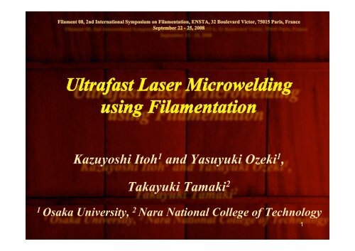
Ultrafast Laser Microwelding using Filamentation - Osaka University
Ultrafast Laser Microwelding using Filamentation - Osaka University
Ultrafast Laser Microwelding using Filamentation - Osaka University

You also want an ePaper? Increase the reach of your titles
YUMPU automatically turns print PDFs into web optimized ePapers that Google loves.
Filament 08, 2nd International Symposium on <strong>Filamentation</strong>, ENSTA, 32 Boulevard Victor, 75015 Paris, France<br />
September 22 - 25, 2008<br />
<strong>Ultrafast</strong> <strong>Laser</strong> <strong>Microwelding</strong><br />
<strong>using</strong> <strong>Filamentation</strong><br />
Kazuyoshi Itoh 1 and Yasuyuki Ozeki 1 ,<br />
Takayuki Tamaki 2<br />
1<br />
<strong>Osaka</strong> <strong>University</strong>, 2 Nara National College of Technology<br />
1
Outline<br />
-Brief introduction to application of<br />
filamentation<br />
- Ultra-fast laser micro-welding of<br />
transparent and<br />
heterogeneous materials<br />
<strong>using</strong> filamentation.<br />
Comparison of nano- and femto-second pulses,<br />
Airtight leak test of hermetic ceiling<br />
2
<strong>Filamentation</strong><br />
- balancing between self-foc<strong>using</strong> and defoc<strong>using</strong> by plasma -<br />
Scattering and/or<br />
luminescence from<br />
filament<br />
Micrograph of the<br />
resultant index<br />
change<br />
Magnified<br />
micrograph<br />
Δn z<br />
= Δn x,y<br />
Δn = 10 -4 ~ 10 -2<br />
3
Applications of filamentation<br />
- Waveguide writing<br />
Waveguides* 1,7 , WG Couplers* 2<br />
- Writing optical elements<br />
Mirrors* 3 , Lenses* 4 , Photonic Devices* 5<br />
- Drilling a hole array * 7<br />
- Welding materials<br />
* 1 K. Yamada, W. Watanabe, T. Toma, K. Itoh, J. Nishii, Opt. Lett. 26, 19 (2001).<br />
* 2 W. Watanabe, T. Asano, K. Yamada, K. Itoh, J. Nishii, Opt. Lett. 28, 2491 (2003).<br />
* 3 K. Yamada et al, Jpn. J. Appl. Phys., 42, Part 1, 6916(2003).<br />
* 4 K. Yamada, W. Watanabe, Y. Li, K. Itoh, and J. Nishii, Opt. Lett,. 29, 1846 (2004) .<br />
* 5 Y. Li, W. Watanabe, T. TamakiI, J. Nishii, and K. Itoh, J. J. Appl. Phys., . 44, 5014 (2005).<br />
* 6 S. Sowa, W. Watanabe, T. Tamaki, J. Nishii, and K. Itoh, Appl. Phys. A, 81,1587 (2005).<br />
* 7 S. Sowa, W. Watanabe, T. Tamaki, J. Nishii, and K. Itoh, Opt. Express 14, 291-297 (2006).<br />
4
- Ultra-fast laser micro-welding<br />
of glass with filaments<br />
T. Tamaki, W.Watanabe, J. Nishii, and K. Itoh, Jpn. J. Appl. Phys., Vol. 44, L687-L689 (2005).<br />
T. Tamaki, W.Watanabe, and K. Itoh, Optics Express, Vol. 14, Issue 22, 10460-10468 (2006).<br />
W. Watanabe, S. Onda, T. Tamaki, and K. Itoh, Appl. Phys. B, Vol. 87, pp. 85-89 (2007).<br />
5
Scanning the filament<br />
Low repetition source<br />
Fast scanning<br />
~ Gap<br />
High repetition source<br />
~ Accumulation of heat<br />
Low repetition<br />
Slow scanning<br />
~ No gap<br />
6
Optical setup<br />
Samples<br />
Fixture<br />
Setup<br />
· Wavelength: 800 nm<br />
· Pulse duration: 130 fs<br />
· Repetition: 1 kHz<br />
· Incidence energy: ~ 1.0 µJ/pulse<br />
Fixture<br />
· Numerical aperture: 0.30<br />
· Irradiation area: 100 µm x 100 µm<br />
· Translation speed: 5.0 µm/s<br />
7
Micrographs of welded silica glass samples<br />
Schematic<br />
Top view<br />
Side view<br />
8
Joining strength (Same material)<br />
Pulse Energy [µJ/pulse]<br />
10<br />
5<br />
15.4<br />
MPa 14.9<br />
MPa<br />
14.9<br />
MPa<br />
0.01<br />
15.3<br />
MPa<br />
15.2<br />
MPa<br />
15.1<br />
MPa<br />
15.2<br />
MPa<br />
15.0<br />
MPa<br />
14.9 MPa<br />
14.9<br />
MPa<br />
14.9<br />
MPa<br />
0.1 1<br />
Scanning Speed [mm/s]<br />
Map of joining strength<br />
Borosilicate glass<br />
Fused silica glass<br />
- 15 MPa ~ 153 kgf/cm 2<br />
- Usual adhesive ~ 50 kgf/cm 2<br />
(kgf: kilogram force)<br />
9
Optical transmittance<br />
81.4 %<br />
85.9 %<br />
87.0 %<br />
Pulse Energy [µJ/pulse]<br />
10<br />
5<br />
86.0 %<br />
87.1 % 88.2<br />
89.0 %<br />
%<br />
0.01<br />
86. 8<br />
%<br />
86.7 %<br />
87.3 %<br />
87.1<br />
%<br />
0.1 1<br />
Scanning Speed [mm/s]<br />
Borosilicate glass<br />
81 ~ 87 %<br />
Theoretical limit: 92 %<br />
Fused silica glass<br />
87 ~ 89 %<br />
Theoretical limit: 93 %<br />
10
Heterogeneous welding:<br />
10<br />
Pulse Energy<br />
[µJ/pulse]<br />
1<br />
0<br />
15.3 MPa 14.9 MPa<br />
15.2<br />
MPa<br />
15.1<br />
MPa<br />
15.2<br />
MPa 15.0<br />
MPa<br />
14.9<br />
MPa<br />
14.9 MPa<br />
15.0<br />
MPa<br />
14.9<br />
MPa<br />
0.1 1<br />
Scanning Speed [mm/s]<br />
Map of joining strength<br />
dissimilar kinds of glass<br />
<strong>Laser</strong><br />
Pulses<br />
Geometry<br />
Borosilicate glass<br />
39* [×10 ‐ /<br />
Fused silica glass<br />
5.9* [×10 ‐ /<br />
*Thermal expansion coefficient<br />
Wataru Watanabe, Satoshi Onda, Takayuki Tamaki,<br />
Kazuyoshi Itoh, and Junji Nishii,<br />
Appl. Phys. Lett., Vol. 89, No. 2, 021106 (2006).<br />
11
Joining strength and transmittance<br />
15.3 MPa 14.9 MPa<br />
71.5 %<br />
73.2 %<br />
10<br />
15.1<br />
MPa<br />
15.0<br />
MPa<br />
10<br />
72.6 % 73.0 %<br />
Pulse Energy<br />
[µJ/pulse]<br />
15.2<br />
MPa<br />
15.0<br />
MPa<br />
14.9<br />
MPa<br />
Pulse Energy<br />
[µJ/pulse]<br />
71.8 %<br />
73.0 %<br />
73.4 %<br />
15.2<br />
MPa<br />
14.9<br />
MPa<br />
72.1 %<br />
73.6 %<br />
14.9<br />
MPa<br />
0.1 1<br />
Scanning Speed [mm/s]<br />
88.3 %<br />
0.1 1<br />
Scanning Speed [mm/s]<br />
Joining strength<br />
Optical transmittance<br />
12
Effects of Annealing ( silica glass & silica glass)<br />
Welded part<br />
Micrograph<br />
before annealing<br />
100 µm 100 µm<br />
Micrograph<br />
after annealing<br />
Annealing makes welded part invisible.<br />
(Implication of disappearance of defects.)<br />
13
Enhancement of joining strength &<br />
optical transmittance<br />
Joining strength Borosilicate glass Fused silica glass<br />
Before<br />
annealing 15 MPa 15 Mpa<br />
After<br />
annealing 33 MPa 33 MPa<br />
Optical transmittance<br />
Before<br />
annealing 88 % 87 %<br />
After<br />
( 336 kgf/cm 2 )<br />
annealing 92 % 91 %:<br />
(Theoretical limit: 93 %) (Theoretical limit: 92 %)<br />
14
Enhancement of optical transmittance<br />
by annealing<br />
Borosilicate glass<br />
Fused silica glass<br />
Before<br />
annealing 88 % 87 %<br />
After<br />
annealing 92 % 91 %<br />
(Theoretical limit: 93 %) (Theoretical limit: 92 %)<br />
15
- Ultra-fast <strong>Laser</strong> Micro-welding of<br />
Glass and Copper<br />
Y. Ozeki, T. Inoue, T. Tamaki, H. Yamaguchi, S. Onda, W. Watanabe, T. Sano,S. Nishiuchi,<br />
A. Hirose, and K. Itoh, Appl. Phys. Express, vol.1, p. 082601, (2008).<br />
K. Itoh and T. Tamaki, SPIE Commercial and Biomedical Applications of <strong>Ultrafast</strong> <strong>Laser</strong>s VIII,<br />
Invited Paper, San Jose Convention Center, San Jose, CA. 20 - 23 January 2008.<br />
K. Itoh and T. Tamaki, PICALO 2008, The 3 rd Pacific International Conference on Application of<br />
<strong>Laser</strong>s and Optics, Invited Paper, April 16 - 18, Capital Hotel, Beijin China, 2008.<br />
16
Heterogeneous welding:<br />
Material<br />
*Thermal expansion coefficient<br />
Polymer<br />
Semiconductor<br />
Metal<br />
Alloy<br />
PMMA<br />
700 [×10 ‐ /<br />
Silicon<br />
28 [×10 ‐ /<br />
Cupper<br />
183 [×10 ‐ /<br />
Stainless steel<br />
175 [×10 ‐ /<br />
dissimilar kinds of materials<br />
Fused silica glass<br />
5.9 [×10 ‐ /<br />
<br />
<br />
<br />
<br />
Successful<br />
Borosilicate glass<br />
39 [×10 ‐ /<br />
<br />
<br />
<br />
<br />
Geometry<br />
<br />
<br />
Wide range of heterogeneous welding<br />
17
Ultra-fast <strong>Laser</strong> Micro-welding of Glass and<br />
Copper<br />
Realizing tight contact<br />
between<br />
glass and copper<br />
18
(a) Side view (b) Top view (c) Whole image<br />
Optical microscope images<br />
<strong>Laser</strong> source: Regenerative Ti:sapphire laser<br />
(Spectra Physics, Spitfire)<br />
Central wavelength: 800 nm<br />
Pulse duration: 130 fs<br />
Repetition rate: 1 kHz<br />
Pulse energy: 4 µJ/pulse<br />
Scan speed: 1 mm/s<br />
Joining strength:<br />
~20 MPa<br />
19
Joining Strength &<br />
Electron Micrograph of Interface<br />
Joining Strength [MPa]<br />
0.4 µJ Average: 21.5 MPa<br />
40<br />
35<br />
30<br />
25<br />
20<br />
15<br />
10<br />
5<br />
0<br />
0.1 1 10<br />
Pulse Energy [µJ]<br />
<br />
Glass<br />
Copper<br />
1 µm<br />
No crack nor gap observed but<br />
some bumpy irregularity presents.<br />
<br />
20
Comparison with ns-pulse welding<br />
30<br />
Joint strength [MPa]<br />
20<br />
10<br />
Femtosecond<br />
pulse<br />
Nanosecond<br />
pulse<br />
< 1/100 reduction<br />
0<br />
10 -1 10 0 10 1 10 2<br />
Pulse energy [µJ]<br />
Lower energy welding is possible by <strong>using</strong> fs pulses.<br />
Femtosecond pulse: 800 nm, 130 fs, 1 kHz<br />
Nanosecond pulse: 527 nm, 600 ns, 1 kHz<br />
Translation speed: 1 mm/s<br />
21
Sample morphology<br />
200 µm<br />
Nanosecond pulse welding<br />
(527 nm, 600 ns, 50 µJ,<br />
1 kHz, 1 mm/s)<br />
Femtosecond pulse welding<br />
(800 nm,
Difference of heat sources<br />
Femtosecond pulses<br />
Nanosecond pulses<br />
Glass<br />
Nonlinear absorption<br />
in filament<br />
(Heating)<br />
Glass<br />
No filament<br />
No absorption<br />
(No heating)<br />
Metal<br />
Linear absorption<br />
(Heating)<br />
Metal<br />
Linear absorption<br />
(Heating)<br />
23
Application of Ultra-fast <strong>Laser</strong> Micro-welding<br />
to Metal Package (Glass & Kovar)<br />
(a) Birds-eye view<br />
(b) Top view<br />
24
Hermetic ceiling of ceramic package<br />
Schott D263 glass<br />
50µm<br />
Ceramic cabity<br />
Electroless<br />
nickel plating<br />
Ceramic package<br />
(92% Alumina)<br />
Welded part<br />
25
Leakage test<br />
Group<br />
<br />
<br />
<br />
<br />
<br />
<br />
<br />
<br />
<br />
<br />
<br />
<br />
1<br />
<br />
<br />
<br />
<br />
<br />
<br />
<br />
<br />
<br />
<br />
<br />
<br />
<br />
2<br />
<br />
<br />
<br />
<br />
<br />
<br />
<br />
<br />
<br />
<br />
<br />
<br />
<br />
<br />
3<br />
<br />
<br />
<br />
<br />
<br />
<br />
<br />
<br />
<br />
<br />
<br />
<br />
<br />
<br />
The results are almost perfect.<br />
26
Summary<br />
-Ultra-fast laser micro-welding of<br />
homogeneous and heterogeneous materials<br />
- silica glass and copper<br />
average joining strength: 21.5 Mpa<br />
( ~220 kgf/cm 2 )<br />
- filaments alleviates the foc<strong>using</strong> requirements<br />
and acts as an important source of<br />
heat for welding.<br />
50µm<br />
27
Coworkers:<br />
Dr. Wataru WATANABE,<br />
Dr. Junji NISHII<br />
National Institute of Advanced Industrial Science<br />
and Technology<br />
Mr. Satoshi Onda<br />
Yokogawa Electric Corporation<br />
Mr. Seiji Sowa<br />
Konica Minolta Opto, Inc.<br />
28