Lect. 13: Dielectric Waveguide (2)
Lect. 13: Dielectric Waveguide (2)
Lect. 13: Dielectric Waveguide (2)

You also want an ePaper? Increase the reach of your titles
YUMPU automatically turns print PDFs into web optimized ePapers that Google loves.
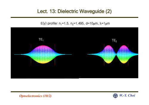
<strong>Lect</strong>. <strong>13</strong>: <strong>Dielectric</strong> <strong>Waveguide</strong> (2)<br />
E(y) profile: n 1 =1.5, n 2 =1.495, d=10μm, λ=1μm<br />
TE 1<br />
TE<br />
1 TE 2<br />
Optoelectronics (10/2)<br />
W.-Y. Choi
<strong>Lect</strong>. <strong>13</strong>: <strong>Dielectric</strong> <strong>Waveguide</strong> (2)<br />
E(y) profile: n 1 =1.5, n 2 =1.495, d=10μm, λ=1μm<br />
TE 1<br />
TE 3<br />
TE<br />
1 TE 2<br />
Optoelectronics (10/2)<br />
W.-Y. Choi
<strong>Lect</strong>. <strong>13</strong>: <strong>Dielectric</strong> <strong>Waveguide</strong> (2)<br />
Wave is not entirely confined within core: Confinement factor<br />
Power inside core<br />
Γ= =<br />
Total Power<br />
d<br />
y= 2<br />
2<br />
∫<br />
d<br />
y=−<br />
2<br />
y=∞<br />
∫<br />
y=−∞<br />
E( y)<br />
E( y)<br />
2<br />
dy<br />
dy<br />
For higher modes, how does Γ change<br />
Optoelectronics (10/2)<br />
W.-Y. Choi
<strong>Lect</strong>. <strong>13</strong>: <strong>Dielectric</strong> <strong>Waveguide</strong> (2)<br />
Partitioning of input field into different guided modes.<br />
n 2<br />
E ( ) in<br />
y<br />
n 1<br />
+ +<br />
Ein( y) ≅ ∑ amEm( y)<br />
n 2<br />
For a , use the fact that E ( y)'s are orthogonal.<br />
m<br />
∫ ∫∑<br />
E ( y ) E ( y ) dy ≈<br />
a E ( y ) ⋅<br />
E ( y )<br />
dy<br />
in m n n m<br />
n<br />
= ∫<br />
∫ in m<br />
∴ am<br />
=<br />
2<br />
∫ E y dy<br />
a E<br />
m<br />
E ( y) E ( y)<br />
dy<br />
m<br />
( )<br />
m<br />
2<br />
m<br />
( y)<br />
dy<br />
m<br />
Optoelectronics (10/2)<br />
W.-Y. Choi
<strong>Lect</strong>. <strong>13</strong>: <strong>Dielectric</strong> <strong>Waveguide</strong> (2)<br />
ω<br />
Slope = c/n 2<br />
Sl / Slope = c/n 1<br />
TE 3<br />
TE 2<br />
TE 2<br />
ω cut-off<br />
TE 1<br />
β m<br />
Schematic dispersion diagram, ω vs. β for the slab waveguide for various TE m . modes.<br />
ω cut–off Group corresponds velocities to V are = π/2. different The group for velocity different v g modes at any => ω is modal the slope dispersion of the ω vs. β<br />
curve at Need that frequency. a single-mode waveguide in order to avoid signal distortion.<br />
How do you design a single mode waveguide<br />
© 1999 S.O. Kasap, Optoelectronics (Prentice Hall)<br />
Optoelectronics (10/2)<br />
W.-Y. Choi
<strong>Lect</strong>. <strong>13</strong>: <strong>Dielectric</strong> <strong>Waveguide</strong> (2)<br />
n 3<br />
cladding<br />
b-V diagram for TE mode<br />
d<br />
n 1<br />
core<br />
n 2<br />
1<br />
2 2 2<br />
0<br />
(<br />
1 2<br />
)<br />
V = kd( kdn − n )<br />
(Normalized k)<br />
b =<br />
⎛β<br />
⎜<br />
⎝ k<br />
n<br />
2<br />
⎞<br />
⎟ − n<br />
⎠<br />
0<br />
2 2<br />
1<br />
−<br />
n<br />
2<br />
2<br />
2<br />
(Normalized β )<br />
b<br />
a =<br />
n<br />
− n<br />
2 2<br />
2 3<br />
2 2<br />
n1 − n2<br />
(Asymmetry factor)<br />
V<br />
Optoelectronics (10/2)<br />
W.-Y. Choi