Testing Virtual ECUs - Power Systems Design
Testing Virtual ECUs - Power Systems Design
Testing Virtual ECUs - Power Systems Design

Create successful ePaper yourself
Turn your PDF publications into a flip-book with our unique Google optimized e-Paper software.
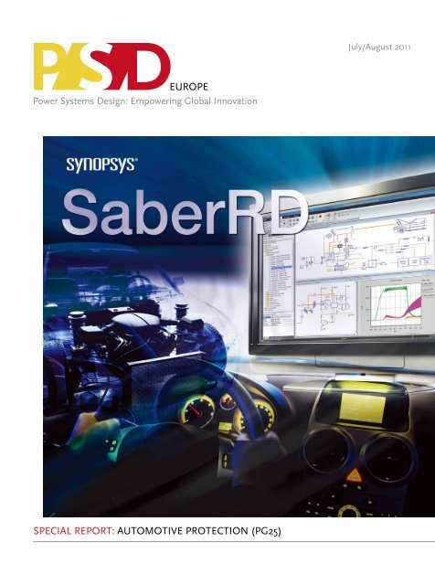
SPECIAL REPORT: AUTOMOTIVE PROTECTION (PG25)<br />
July/August 2011
36V, 4A Sync Buck<br />
VIN = 4.5V to 36V<br />
(Transients to 60V)<br />
The LT<br />
Features<br />
Info & Free Samples<br />
®<br />
3690 brings a new level of performance and features for high voltage point-of-load step-down conversion. Its wide<br />
input voltage range of 3.9V to 36V, with 60V transients, meets the needs of many of the rails common to industrial, medical<br />
and automotive applications. Up to 4A of continuous output current can be supplied to the load with minimal thermal design.<br />
Its The 70µA simplest of quiescent functions current are often in standby the most maximizes difficult to battery design. life The in current “always-on” source—a applications. basic circuit With element—has up to 1.5MHz not switching been<br />
frequency available and as an a high IC. Discrete level of implementations integration, the suffer external from components poor accuracy, are few high and TC small, or complexity. enabling Our a compact new current solution source, footprint. the<br />
LT<br />
LT3690 Demo Circuit<br />
® A Simple, Precise 2-Terminal Current Source<br />
3092, provides all the performance without the compromises: programmable up to 200mA, high AC and DC impedance,<br />
low TC and no capacitors required. Its two floating terminals make it easy to use in precision or remote current limiting, bias<br />
circuits, intrinsic safety circuits, temperature sensing, active load and signaling applications.<br />
• Input Voltage Range:<br />
3.9V to 36V (60V Transients)<br />
• 4A of Continuous Output Current<br />
• Quiescent Current of 70µA<br />
(12VIN to 3.3VOUT) • Low Output Ripple of
2SP0115T Gate Driver<br />
Unleash the full power of your converter design using<br />
the new 2SP0115T Plug-and-Play driver. With its<br />
direct paralleling capability, the scalability of your<br />
design into highest power ratings is unlimited.<br />
Rugged SCALE-2 technology enables the complete<br />
driver functionality on a single PCB board, exactly fitting<br />
the size of 17mm dual modules.<br />
Combined with the CONCEPT advanced active clamping<br />
function, the electrical performance of the IGBT<br />
can be fully exploited while keeping the SOA of the<br />
IGBT. Needless to say that the high integration level<br />
provides the best possible reliability by a minimzed<br />
number of components.<br />
CT-Concept Technologie AG, Renferstrasse 15, CH-2504 Biel, Switzerland, Phone +41-32-344 47 47<br />
Unleash<br />
Sheer <strong>Power</strong>!<br />
SAMPLES AVAILABLE!<br />
Features<br />
Plug-and-Play solution<br />
1W output power<br />
15A gate current<br />
4<br />
VIEWpoint<br />
AGS Media Group<br />
146 Charles Street<br />
Annapolis, MD 21401 USATel:<br />
+410.295.0177<br />
Fax: +510.217.3608<br />
www.powersystemsdesign.com<br />
Editor-in-Chief<br />
Cliff Keys<br />
cliff.keys@powersystemsdesign.com<br />
Contributing Editors<br />
Liu Hong, Editor-in-Chief, <strong>Power</strong> <strong>Systems</strong><br />
<strong>Design</strong> China<br />
powersdc@126.com<br />
Ash Sharma, IMS Research<br />
Ash.sharma@imsresearch.com<br />
Dr. Ray Ridley, Ridley Engineering<br />
RRidley@ridleyengineerng.com<br />
David Morrison, How2<strong>Power</strong><br />
david@how2power.com<br />
Publishing Director<br />
Jim Graham<br />
jim.graham@powersystemsdesign.com<br />
Publisher<br />
Julia Stocks<br />
Julia.stocks@powersystemsdesign.com<br />
Circulation Management<br />
Kathryn Philips<br />
Kathryn.phillips@powersystemsdesign.com<br />
Research Director<br />
Meghan Corneal<br />
meghan.corneal@powersystemsdesign.com<br />
Magazine <strong>Design</strong><br />
Louis C. Geiger<br />
louis@agencyofrecord.com<br />
Production Manager<br />
Chris Corneal<br />
chris.corneal@powersystemsdesign.com<br />
Registration of copyright: January 2004<br />
ISSN number: 1613-6365<br />
AGS Media Group and <strong>Power</strong> <strong>Systems</strong> <strong>Design</strong><br />
Europe magazine assume and hereby disclaim<br />
any liability to any person for any loss or damage<br />
by errors or ommissions in the material<br />
contained herein regardless of whether such<br />
errors result from negligence, accident or any<br />
other cause whatsoever.Send address changes<br />
to: circulation@powersystemsdesign.comFree<br />
Magazine Subscriptions,<br />
go to: www.powersystemsdesign.com<br />
Volume 8, Issue 6<br />
WWW.POWERSYSTEMSDESIGN.COM<br />
POWER SYSTEMS DESIGN<br />
Welcome to this issue of PSD Europe where we are featuring automotive electronics. With the<br />
rise in oil prices and the heightened ecological sensitivity in the public domain, driven by the<br />
mass media, HEVs and EVs are fast becoming a commercial viability. This is great news for<br />
the power industry and great for future generations. Also, with the political uncertainty and<br />
volatility of oil production outside of the US, many are concluding that electric power is the<br />
way forward for our automobiles.<br />
There are of course, challenges. Many of them you can read in this issue of PSD, aimed at<br />
giving you solutions. The visionaries are talking about infrastructure for widespread charging<br />
while power engineers working out how to design the new vehicles with all its drive, control<br />
and power issues presented by the battery management, lighting and electronic control for all<br />
the electronics. Quite a challenge, especially given the limited range - but it will get there in<br />
the end, power engineers will fix it.<br />
But what a wonderful project for any power engineer; working on a vehicle that is clean, in<br />
terms of emissions, with the new LED lighting systems and a new control system. This is a<br />
project with a wonderful legacy for mankind. I just hope they can build them cheap enough.<br />
It’s no wonder that Fairchild have decided to build a R&D centre in Southern Germany, right<br />
where the big automotive firms are.<br />
After making major inroads into the desktop market, quad-core PC microprocessors now<br />
are set to conquer the notebook segment with about half of the mobile computers shipped<br />
in 2015 expected to employ these advanced chips according to IHS. The recently introduced<br />
graphics-enabled microprocessor places the graphics processor on the processor die. These<br />
microprocessors will be found in excess of 90% of notebooks sold in 2015 delivering improved<br />
power management of the on-chip graphics unit, although in terms of graphics performance,<br />
are not able to outperform discrete graphics cards. Again, power is the key.<br />
Audi has demonstrated a device along with Qualcomm and Peiker that allowed for the wireless<br />
charging of smart phones, personal digital assistants (PDAs) and other devices. The<br />
wireless charging solution would be sold as an accessory by Audi.<br />
Meanwhile, at Volkswagen’s new Electronics Research Laboratory in Silicon Valley, research is<br />
being conducted on a centre console that can wirelessly charge smart phones, similar to the<br />
power mats now on the market for home use. The project, in development with Qualcomm,<br />
reportedly could use magnetic near-field resonance to power rear-seat entertainment or ambient<br />
lighting systems as well.<br />
I do hope you enjoy the magazine, please keep the feedback coming, and do check out Dilbert<br />
at the back of the magazine.<br />
All the best<br />
Cliff<br />
Editorial Director & Editor-in-Chief<br />
<strong>Power</strong> <strong>Systems</strong> <strong>Design</strong><br />
Cliff.Keys@powersystemsdesign.com<br />
AUTOMOTIVE<br />
INVESTS<br />
POWERline<br />
POWER SYSTEMS DESIGN JULY/AUGUST 2011<br />
DESIGN TOOLS FOR EV/HEV<br />
Simulation and test expert firm,<br />
dSPACE, is in the business of<br />
developing tools for the design of<br />
electronic control units (<strong>ECUs</strong>) and<br />
mechatronic systems.<br />
<strong>Testing</strong> <strong>Virtual</strong> <strong>ECUs</strong><br />
The virtual ECU, or<br />
V-ECU, comprises<br />
components from the<br />
application and the basic software,<br />
and provides functionalities<br />
comparable to those of a real<br />
ECU. Unlike a soft ECU, which<br />
uses only a simplified Simulink®/<br />
Stateflow® model, a V-ECU<br />
usually has the same software<br />
components that will run on<br />
the finished ECU. There is no<br />
strict dividing line between a soft<br />
ECU and a V-ECU, but a V-ECU<br />
generally represents the real ECU<br />
more realistically.<br />
Customers can use virtual ECU<br />
models for testing and validation<br />
throughout the ECU development<br />
process. The term 'virtual ECU<br />
testing' covers all simulation<br />
scenarios in which virtual <strong>ECUs</strong><br />
are used.<br />
Today's ECU software comprises<br />
numerous software components<br />
(SWCs) with intensive interactions.<br />
In the large ECU networks<br />
frequently installed in current<br />
vehicles, the number of SWCs can<br />
easily reach the thousands, and<br />
because the task of developing<br />
ECU components is usually shared<br />
by several departments or even<br />
different companies, not only<br />
the SWCs themselves have to be<br />
tested and validated, but also the<br />
interactions between them.<br />
Early <strong>Testing</strong> Without Hardware<br />
Previously, the testing and<br />
validation of ECU software could<br />
not even begin until the prototype<br />
<strong>ECUs</strong> were available. With virtual<br />
ECU testing (VET), the SWCs,<br />
which are already available, are<br />
combined to create a virtual ECU<br />
model. This is then tested and<br />
validated in offline simulation<br />
on a standard PC. This lets<br />
developers investigate real-world<br />
issues such as task scheduling,<br />
the behavior of the basic software,<br />
and communication behavior on a<br />
virtual CAN bus<br />
Simulating EV/ HEV Drives<br />
The dSPACE ASM Electric<br />
Components simulation package<br />
is now supported by JMAG, a<br />
Finite Element Analysis (FEA)<br />
tool for electromechanical<br />
design developed by the JSOL<br />
Corporation. Automotive<br />
Simulation Models (ASM) electric<br />
components are designed for the<br />
real-time simulation of vehicle<br />
electrical systems or hybrid<br />
drivetrains.<br />
With JMAG, users can now<br />
define the key characteristics of<br />
electric motors and export them<br />
to parameterize the generic ASM<br />
electric motor models. After virtual<br />
electric motors are defined, they<br />
can be executed on a hardwarein-the-loop<br />
(HIL) simulator in<br />
real time. The tool coupling<br />
gives users convenient graphical<br />
designs of complex systems and<br />
real-time performance. The easy<br />
workflow and high precision speed<br />
up developments and ensure the<br />
highest quality.<br />
www.dspace.com<br />
WWW.POWERSYSTEMSDESIGN.COM<br />
5
6<br />
POWERplayer<br />
GOOD NEWS TIME<br />
WWW.POWERSYSTEMSDESIGN.COM<br />
Reported by Cliff Keys, Editorial Director & Editor-in-Chief, <strong>Power</strong><br />
<strong>Systems</strong> <strong>Design</strong><br />
I had the pleasure to meet with Thomas Neyer,<br />
Vice President of High Voltage Semiconductor<br />
Technology at Fairchild Semiconductor, to discuss the setup of<br />
the company’s new High Voltage R&D Centre in Munich.<br />
P<br />
rior to working at<br />
Fairchild, Thomas<br />
served at Grace<br />
Semiconductor in<br />
Shanghai as EVP and Head of<br />
R&D and Fab Operation with the<br />
Vision to build the first Foundry<br />
for differentiated Technologies<br />
in Asia. Thomas holds a PhD<br />
in Physics from the Vienna<br />
University of Technology.<br />
This was an enjoyable meeting<br />
for me personally with the<br />
announcement of Fairchild’s<br />
new High Voltage R&D Centre,<br />
which will develop innovative<br />
products for the automotive and<br />
industrial markets. Thomas is<br />
now evaluating the availability of<br />
suitable premises to house the<br />
company’s exciting new venture.<br />
Thomas explained to me, that<br />
with the focus on Electric and<br />
Hybrid Electric Vehicles to use<br />
clean energy with low emissions,<br />
Fairchild is well placed to exploit<br />
this lucrative market. At the<br />
moment Japanese suppliers have<br />
over 50% of the HEV market<br />
share, but by 2016 strategy<br />
analysts predict that the EV<br />
market will be more uniformly<br />
spread. The opportunity for<br />
Fairchild is immense. Hence the<br />
applaudable investment in this<br />
R&D centre.<br />
The scope of the new centre will<br />
include:<br />
• Device and process<br />
simulation<br />
• <strong>Design</strong> and layout<br />
• Characterization and testing<br />
lab<br />
• Process integration, device<br />
architecture,<br />
• New materials and module<br />
development.<br />
For the initial phase, Fairchild is<br />
currently building the team for<br />
the start-up of this inspirational<br />
and expanding centre in Munich<br />
including fundamental and<br />
scientific research which has a<br />
high strategic impact and priority<br />
within this successful global<br />
company.<br />
The mission of this team will<br />
be to advance Fairchild’s power<br />
technology and product portfolio<br />
for High Voltage applications<br />
for Industrial, Automotive and<br />
Consumer markets to take over<br />
the leading-edge position in the<br />
industry.<br />
The newly formed R&D centre<br />
will liaise closely with existing<br />
global Fairchild Technologists in<br />
US, Sweden and Korea, as well<br />
as to work in partnership with<br />
Research institutes and hand<br />
selected partnership programs<br />
with competitors.<br />
The start-up team of the new centre<br />
will address next generation IGBT and<br />
SuperJunction device concepts utilizing<br />
state-of-the-art process and device<br />
simulation techniques, establishing new<br />
processing modules in Fairchild’s advanced<br />
6/8” manufacturing plants and focusing<br />
on improved device ruggedness and key<br />
figures of merit. Hence, wafer level device<br />
characterization, modelling expertise and<br />
advanced high power packaging expertise<br />
will be established accordingly.<br />
For the mid-term horizon, more efforts are<br />
being assigned to pursue development of<br />
wide bandgap switches and rectifiers, which<br />
are predicted to take over significant market<br />
share for high power and high efficiency<br />
types of application in the second half of this<br />
decade. Fairchild is certainly in this for the<br />
long-haul.<br />
Notably, in order to seize a head start in<br />
this, Fairchild has recently acquired TranSiC<br />
in Stockholm, which owns significant IP<br />
and expertise in SiC technology. Moreover,<br />
Fairchild is assessing several options to make<br />
a bold move into GaN technology where the<br />
R&D centre in Munich will be instrumental<br />
to mature and commercialize new product<br />
lines.<br />
Certainly this is good news for Fairchild, and<br />
great news for our industry.<br />
www.fairchildsemi.com<br />
Superior Solutions<br />
for Automotive<br />
• Multilayer ceramic chip capacitors for<br />
high-temperature applications<br />
• Aluminum electrolytic and film capacitors with<br />
high vibration stability<br />
• <strong>Power</strong> Capacitor Chip (PCC) with volume<br />
fill factor of nearly 1<br />
• Piezo actuators for fuel-saving injection systems<br />
• Common-mode filters for CAN bus and FlexRay<br />
• SMT power inductors up to 150 °C<br />
• Space-saving power transformers<br />
• Current sensors with high accuracy for EV<br />
• Transponder coils for TMPS<br />
• Self-regulating PTC heating elements<br />
• Customized NTC and PTC thermistors<br />
• Miniaturized pressure sensors up to 25 bar<br />
• Gear tooth sensors for angle and speed sensing<br />
• SAW components for telematics, RKE and TPMS<br />
• Multilayer varistors for ESD and transient protection<br />
• Switching spark gaps for Xenon head lights<br />
www.tdk-epc.com TDK-EPC Corporation<br />
SPS / IPC / DRIVES • Nuremberg, Germany<br />
November 22 to 24, 2011 • Hall 4, Stand 160
8<br />
MARKETwatch<br />
AUTOMOTIVE INDUSTRY WILD<br />
WEST: SILICON SLINGERS AND<br />
ELECTRIC SALOONS<br />
WWW.POWERSYSTEMSDESIGN.COM<br />
By Alastair Hayfield, Research Director, Automotive and Transport, IMS<br />
Research<br />
It is rare to get a glimpse into the past, but<br />
researching the electric vehicle industry at the<br />
moment gives a fascinating insight into the<br />
twilight years of the 19th century when Diesel, Benz, and<br />
others were leaving their indelible mark on a coming century<br />
of automotive transport.<br />
E<br />
lectric vehicles are<br />
nothing new; but like<br />
those early years,<br />
now is a ‘wild’ time<br />
of innovation, exploration<br />
and just a little uncertainty.<br />
There are different opinions on<br />
implementation – should we go<br />
full battery or hybrid? What type<br />
of hybrid? There are different<br />
views on charging – AC? DC?<br />
Fast or slow? And everybody<br />
knows that their design will be<br />
the next Model T.<br />
So what can the past tell us<br />
about the future?<br />
Opportunity breeds innovation<br />
and vice-versa. There is clear<br />
and growing demand for electric<br />
vehicles regardless of type (a<br />
forecast 15% of light vehicles<br />
produced in 2021 will be ‘electric’,<br />
versus 1.5% in 2010 according<br />
to IMS Research), prompting<br />
vehicle OEMs, tier1s, and other<br />
suppliers in the supply chain to<br />
join the electric bandwagon.<br />
Compared with ‘regular’ internal<br />
combustion engine vehicles,<br />
hybrid and electric vehicles<br />
require far higher semiconductor<br />
content, most notably for the<br />
battery management system<br />
and the inverter used to drive<br />
the main electric motor(s).<br />
IMS Research estimates that<br />
the semiconductor content per<br />
electric vehicle drivetrain will be<br />
over $600 in 2021.<br />
By 2021, IMS Research forecasts<br />
that the semiconductor<br />
opportunity in electric vehicle<br />
drivetrains will approach<br />
US$10bn. Much of this growth is<br />
being fuelled by power discretes,<br />
the core components at the heart<br />
of the electric vehicle inverter<br />
and AC/DC power supply unit.<br />
In fact, total sales of power<br />
discretes and modules is forecast<br />
to top US$8bn in 2021.<br />
The battery management<br />
system is another area where<br />
semiconductor vendors are<br />
‘eyeing’ their prospects. Li-ion<br />
battery technology looks set<br />
to be the de facto ‘standard’<br />
for storing power on board<br />
electric vehicles. Less stable
© National Semiconductor Corporation, 2011. National Semiconductor, , <strong>Power</strong>Wise, and WEBENCH are registered trademarks. All rights reserved. Complex<br />
LED<br />
<strong>Systems</strong>.<br />
Easy <strong>Design</strong>.<br />
<strong>Design</strong> Tool Creates Optimized Lighting <strong>Systems</strong><br />
in Minutes<br />
National Semiconductor’s WEBENCH ® LED Architect<br />
tool addresses temperature and current variation<br />
affecting light output and LED lifetime by helping<br />
determine the optimal design for your desired lumen<br />
output. Specify, review real-time tradeoffs, generate<br />
your prototype, and evaluate it – all in minutes.<br />
q<br />
national.com/LED<br />
than NiMH, Li-ion batteries require significantly<br />
more battery management (temperature<br />
monitoring, cell balancing, etc.) which increases<br />
the semiconductor content. IMS Research<br />
estimates that the semiconductor content of a<br />
LI-ion battery is currently five times that of an<br />
equivalent NiMH battery, with the majority of<br />
the difference coming from the number of ASSPs<br />
needed for cell pack voltage monitoring.<br />
Automotive OEMs have considerable intellectual<br />
property tied up in the design of their internal<br />
combustion engines. The same is true for<br />
hybrid and electric vehicles on the market at<br />
the moment, with the theory being that electric<br />
motor control is one way of keeping expertise inhouse.<br />
But is this really the ideal way of getting<br />
the most out of an electric vehicle?<br />
Much of the expertise needed to control high<br />
speed electric motors can be found in the<br />
industrial automation or motor industry. Players<br />
in these markets are setting their sights on the<br />
electric vehicle market, particularly with ‘offthe-shelf’<br />
inverter modules. Not only do these<br />
‘modules’ play to their strengths, but they give<br />
vehicle OEMs the opportunity to reduce R&D<br />
costs by outsourcing motor control design.<br />
The automotive OEMs have a big decision to<br />
make: do they go it alone on motor control<br />
design to retain the “engine IP”, or do they work<br />
with existing experts to take advantage of their<br />
experience?<br />
www.imsresearch.com<br />
DESIGNtips<br />
POWER SYSTEMS DESIGN JULY/AUGUST 2011<br />
POWER SUPPLY DEVELOPMENT<br />
DIARY PART XIV<br />
By Dr. Ray Ridley<br />
This article continues the series in which Dr.<br />
Ridley documents the processes involved in<br />
taking a power supply from the initial design to<br />
the full-power prototype. The second layout of the PC board<br />
incorporates significant changes in the power stage, changing<br />
the number of outputs from three to five. Some of the issues<br />
involved in the coupled-inductor magnetics design are<br />
discussed.<br />
T<br />
hree Output Coupled-<br />
Inductor <strong>Design</strong><br />
The original<br />
specification for the<br />
power supply design was as<br />
follows:<br />
1. Output 1 – 35 VDC @ 10A<br />
isolated<br />
2. Output 2 – 35 VDC @ 10 A<br />
isolated<br />
3. Output 3 – 15 VDC Bias<br />
power and regulated output,<br />
primary referenced<br />
4. Maximum power 350 W (only<br />
one output fully loaded at<br />
a time, application is for<br />
audio.)<br />
5. Input – 180 – 265 AC<br />
6. <strong>Power</strong> Topology: Two-switch<br />
forward<br />
Figure 1 shows the schematic<br />
of the three-output forward<br />
Figure 1: Forward Converter with Three Coupled-Inductor Outputs<br />
converter. A single core inductor<br />
is used with three windings,<br />
one for each of the outputs.<br />
This coupled-inductor approach<br />
provides the best cross-regulation<br />
between each of the outputs.<br />
There are two major advantages<br />
of coupled inductors – firstly, all<br />
of the outputs are tied together<br />
through the transformer action<br />
of the inductor, preventing them<br />
from having individual resonant<br />
frequencies. Secondly, regardless<br />
of individual loading on each<br />
of the outputs, the coupled<br />
inductor forces all of the outputs<br />
WWW.POWERSYSTEMSDESIGN.COM<br />
11
12<br />
DESIGNtips<br />
Figure 2: Three-Output Transformer Winding Layout<br />
to be in either continuous or<br />
discontinuous mode concurrently,<br />
greatly improving the regulation.<br />
As shown in an earlier part of this<br />
series, excellent regulation was<br />
achieved with a wide variation of<br />
output loading.<br />
Figure 2 shows the winding<br />
layout for the three-output<br />
transformer. The first layer of<br />
winding was the first secondary<br />
output, consisting of 15 turns<br />
wound with triple-insulated<br />
kapton wire. This winding used<br />
a single strand of wire, with a<br />
gauge selected to exactly fill one<br />
layer of the bobbin. One layer of<br />
magnetics tape was added on<br />
top of this secondary to provide<br />
a smooth winding surface for the<br />
subsequent windings.<br />
The next layer of winding is a<br />
single layer primary with 45 turns<br />
of magnet wire, followed by a<br />
layer of tape. The third layer is<br />
the other high-power secondary,<br />
followed by 6 turns on the final<br />
layer for the bias supply and<br />
regulation winding. For coupled<br />
designs, the lowest power<br />
winding is placed on the outside<br />
Figure 3: Three-Output Coupled-Inductor Winding<br />
Layout<br />
of the winding sequence for best<br />
cross-regulation.<br />
Figure 3 shows the winding<br />
layout of the coupled inductor.<br />
Notice from the schematic of<br />
Figure 1 that the turns ratios of<br />
the inductor and transformer are<br />
critical, and the ratio between the<br />
different secondaries must match<br />
exactly. Hence the transformer<br />
has a ratio of 15:15:6 for the<br />
secondaries, and this exactly<br />
matches the turns count for the<br />
inductor. Apart from this caution,<br />
the design of a coupled inductor<br />
is not particularly difficult. The<br />
simplest approach is to design<br />
the inductor as though it were a<br />
single-output design rated at the<br />
power of the sum of the three<br />
outputs. This sets the required<br />
number of turns for the inductor<br />
value required with the selected<br />
core area.<br />
The layout of the inductor in<br />
this case is the same as the<br />
transformer, starting with each<br />
of the high power secondaries,<br />
and finishing with the bias<br />
winding. Notice that the bias<br />
winding, which is<br />
primary referenced,<br />
is the one with the<br />
triple-insulated kapton<br />
wire. This reduces<br />
cost of materials<br />
and processing time<br />
during the inductor<br />
construction.<br />
Five-Output Coupled-<br />
Inductor <strong>Design</strong><br />
The original plan for<br />
this project was to provide two<br />
main power outputs, and one<br />
regulation winding. A second<br />
power supply was to be used to<br />
provide the exact same outputs<br />
to a second load amplifier of a<br />
stereo pair.<br />
However, during system testing,<br />
it became clear that the final load<br />
was less than expected, and that<br />
all four outputs could possibly<br />
be provided with a single power<br />
stage. A decision was made<br />
during the second board layout<br />
to incorporate this change into<br />
the design, providing five outputs<br />
from a single forward converter.<br />
The schematic of the five-output<br />
converter is shown in Figure 4.<br />
This is a significant change<br />
Figure 4: Redesigned Forward<br />
Converter with Five Coupled-<br />
Inductor Outputs<br />
to the project, but one which<br />
provides substantial savings<br />
in parts, board area, and cost.<br />
The risk is in whether the tight<br />
cross-regulation is lost with more<br />
outputs. The new design also<br />
presents something of a technical<br />
challenge during the board<br />
layout. One of the significant<br />
complications of coupledinductor<br />
designs is managing<br />
the multiple connections of the<br />
transformer, the inductor,<br />
and the rectifier diodes on<br />
the printed circuit board.<br />
The extra outputs also<br />
present significant changes<br />
to the transformer and<br />
inductor designs. There are<br />
now a total of six windings<br />
in the transformer, and<br />
changes must be made to<br />
accommodate the extra<br />
complexity. Figure 5 shows the<br />
winding layout of the transformer.<br />
The first two secondaries are<br />
wound bifilar with each other to<br />
exactly fill the layer with 13 turns<br />
on each secondary of magnet<br />
wire.<br />
The turns count was reduced<br />
because the primary layer could<br />
no longer accommodate the<br />
same 45 turns as before in the<br />
bobbin. With more secondaries,<br />
it made better manufacturing<br />
sense to use triple-insulated<br />
Figure 5: Five-Output Transformer Winding Layout<br />
wire for the primary rather than<br />
the secondaries. Only 38 turns<br />
could fit in the layer neatly. This<br />
POWER SYSTEMS DESIGN JULY/AUGUST 2011<br />
reduced turns count raises the<br />
core excitation, and the switching<br />
frequency must also be raised<br />
slightly to 250 kHz from 200 kHz<br />
in order to avoid saturation of<br />
the transformer.<br />
After the primary is wound, the<br />
remaining two secondaries are<br />
placed on top of this, wound<br />
bifilar with each other. Five turns<br />
of the bias winding complete the<br />
transformer design.<br />
The secondary turns ratio of the<br />
transformer is now 13:13:5, and<br />
this ratio must be maintained<br />
exactly in the inductor. For the<br />
previous inductor design, 15<br />
turns were used in the inductor<br />
main outputs, but this pushed<br />
the design hard in terms of flux<br />
level, and only 20 µH inductance<br />
could be used, resulting in<br />
significant output ripple.<br />
With the reduced power<br />
requirements observed in the<br />
system testing, a decision was<br />
made to raise the turns count<br />
on the main output to 26. This<br />
allowed a larger inductance of<br />
30 µH with a reduced core flux<br />
WWW.POWERSYSTEMSDESIGN.COM WWW.POWERSYSTEMSDESIGN.COM<br />
13
14<br />
DESIGNtips<br />
Figure 6: Five-Output Coupled-Inductor Winding Layout<br />
level. The value of 26 was chosen<br />
since it allows us to exactly the<br />
match the transformer turns<br />
ratio when 10 turns are placed<br />
on the bias winding of the<br />
inductor. Normally for a forward<br />
converter inductor, the value<br />
of inductance and the number<br />
of turns are determined by the<br />
current level and core area. In<br />
the case of the coupled inductor<br />
design, however, maintaining the<br />
proper turns ratio is paramount,<br />
and the number of turns is set<br />
by this requirement. This allows<br />
the value of inductance to be<br />
increased as a consequence.<br />
It must be remembered that in<br />
magnetics design, we have many<br />
degrees of freedom, and there<br />
are no hard rules determining the<br />
value of an output inductor. It is<br />
important not to overconstrain<br />
thinking, a common error<br />
of many design books on<br />
magnetics. For example,<br />
many texts will fix the value of<br />
inductance to give a specified<br />
ripple current, but this removes<br />
freedom for the designer to<br />
choose a value that, in reality,<br />
WWW.POWERSYSTEMSDESIGN.COM<br />
can be varied over a significant<br />
range without detriment to the<br />
overall performance.<br />
The layout of the new inductor is<br />
shown in Figure 6. Each winding<br />
occupies a single layer of the<br />
inductor, with the wire gauge<br />
choses to exactly fill the layer<br />
neatly. The final layer is the 10<br />
turns of bias winding, using<br />
triple insulated wire.<br />
Summary<br />
The turn of a PC board is usually<br />
a major project milestone. It<br />
presents the opportunity to clean<br />
up previous errors in a board,<br />
improve manufacturability, and<br />
move a step further towards a<br />
final product.<br />
However, in many projects, the<br />
PC board iteration is often seen<br />
as an opportunity to revisit<br />
project goals, and make major<br />
changes to a design project<br />
and its specifications. In this<br />
particular project, a large number<br />
of changes have been made, and<br />
the risk of incorporating these<br />
changes has to be balanced<br />
against the potential gains in the<br />
final product. The risk here is not<br />
too great since there is always<br />
the option of reverting back to<br />
the previous design of just three<br />
outputs if the regulation achieved<br />
during testing is insufficient.<br />
It must be stated, however,<br />
that substantial changes to<br />
components, especially the<br />
magnetics, will result in the<br />
need to reiterate much of the<br />
testing of the power supply,<br />
and the time to do this must<br />
not be underestimated. The<br />
changed turns of the transformer<br />
and inductor will affect the<br />
cross-regulation, EMI, ringing,<br />
snubbers, current protection, and<br />
semiconductor stresses.<br />
If the second iteration had<br />
been undertaken with none of<br />
these changes, and the design<br />
remained unchanged with three<br />
outputs, there is a reasonable<br />
expectation that this would be the<br />
final PC layout before production.<br />
However, the substantial changes<br />
make it likely that a third layout<br />
pass will be needed before<br />
finishing the design.<br />
Author: Dr. Ray Ridley<br />
President<br />
Ridley Engineering<br />
www.ridleyengineering,com<br />
POWER SYSTEMS DESIGN JULY/AUGUST 2011<br />
MULTI-DOMAIN SIMULATION<br />
Automotive power electronics components and systems<br />
By Thorsten Gerke & Kurt Mueller<br />
Electrification is driving the need for comprehensive multidomain<br />
system simulation in hybrid-electric and electric<br />
vehicles.<br />
A<br />
Cover Story<br />
vehicle’s power<br />
electronic<br />
components, coupled<br />
with the overall<br />
power management and control<br />
system, introduces a new set<br />
of challenges for electrical<br />
system design. These power<br />
electronic components include:<br />
energy storage devices (such as<br />
batteries, ultracapacitors), DC/DC<br />
converters, inverters, and drives.<br />
SaberRD, the latest addition to the<br />
Synopsys® automotive product<br />
portfolio, is designed for modeling<br />
and simulating power electronics<br />
with a focus on addressing the<br />
challenges of integrated power<br />
system design and validation.<br />
The combination of electrical<br />
drive systems to traditional low<br />
voltage power networks takes the<br />
design challenge of vehicle level<br />
efficiency to new dimensions.<br />
Weight, aerodynamics and engine<br />
efficiency have always been a<br />
significant consumer of vehicle<br />
power. In today’s complex vehicle<br />
designs, the electrothermal and<br />
Figure 1: Structure of the SaberRD environment<br />
electromagnetic behavior of DC/<br />
DC converters, electric motors,<br />
and drives are a significant<br />
piece of overall vehicle power.<br />
Consumer demands for greater<br />
fuel efficiency, reduced carbon<br />
footprint along with traditional<br />
vehicle performance require new<br />
and creative trade-offs between<br />
important system characteristics<br />
that can only be done at an<br />
integrated, multi-domain level.<br />
During a panel discussion at<br />
Convergence 2010 in Detroit,<br />
Michigan, Senior Chief Engineer<br />
from Honda, Yoshio Suzuki,<br />
emphasized that carmakers need<br />
more support from software<br />
providers to help them model and<br />
simulate complete systems in an<br />
electronics context. SaberRD was<br />
developed specifically to target this<br />
need: an intuitive tool for power<br />
electronics design, validation and<br />
system integration built upon 25<br />
years of experience and success in<br />
the power electronics industry.<br />
The complexity of modeling and<br />
simulating physical systems<br />
can be daunting, especially for<br />
someone coming from a less<br />
power-electronics focused point of<br />
view. As a result, tool developers<br />
are faced with a delicate balancing<br />
WWW.POWERSYSTEMSDESIGN.COM<br />
15
16<br />
Cover Story<br />
act – making the product simple<br />
and intuitive to use so that even<br />
novices can quickly and effectively<br />
simulate, but capable enough<br />
to deliver accurate simulation<br />
results. To guide users through<br />
a simulation-based development<br />
project, SaberRD uses a<br />
modern integrated development<br />
environment (IDE) to step users<br />
from initial design creation<br />
through to the final analysis and<br />
interpretation of simulation results.<br />
The environment includes four<br />
primary modules (see Figure 1):<br />
• Circuit and system design<br />
for defining the system<br />
topology as schematics of<br />
interconnected multi-domain<br />
blocks<br />
• Modeling and characterization<br />
for fast, accurate development<br />
of simulation models including<br />
power semiconductor devices<br />
(IGBTs, MOSFETs, diodes),<br />
electrical machines, control<br />
blocks, and a variety of<br />
additional effects to account<br />
for thermal, magnetic, and<br />
other behaviors of interest<br />
• Simulation and test<br />
procedures for intuitively<br />
creating test benches, defining<br />
test scenarios and analyzing<br />
worst-case scenarios<br />
• Analysis and reporting with<br />
logging of measurements and<br />
the automated evaluation of<br />
system robustness and quality<br />
including thermal, electrical<br />
and magnetic losses, efficiency<br />
metrics, and statistical<br />
distributions<br />
Intuitive and Flexible Modeling<br />
The key to capturing integrated<br />
physical behavior of a system is<br />
to have accurate and appropriate<br />
simulation models available. In<br />
order to accurately quantify the efficiency<br />
of an electric drive system,<br />
it is best to model the system in<br />
a single simulation environment.<br />
This environment needs to incorporate<br />
important loss mechanisms<br />
such as magnetic effects (saturation,<br />
thermal dependencies),<br />
electrical effects (electro-thermal<br />
coupled transistor behavior),<br />
mechanical loading, along with<br />
control algorithms. In automotive<br />
power electronics, self-heating<br />
behavior and statistical production<br />
variation can give rise to unpredictable<br />
complex system interactions.<br />
Inclusion of these physical<br />
domains allows for optimization<br />
at the component, sub-system,<br />
system and control software levels<br />
to meet overall vehicle design<br />
criteria.<br />
Modeling these behaviors is difficult<br />
- how does one go from physical<br />
devices to models with enough<br />
detail to accurately describe system<br />
behavior? Primary challenges<br />
include access to proprietary data<br />
about particular components or<br />
subsystems, inclusion of enough<br />
detail for system relevant quantities<br />
(e.g. thermal effects on electrical<br />
signals) without overly complicated<br />
formulas (e.g. co-dependent<br />
equations based on physics first<br />
principles), and methods for validating<br />
that the model is accurate.<br />
SaberRD addresses these modeling<br />
needs with an extensive library<br />
of over 30,000 physical models in<br />
all domains mentioned as well as<br />
providing graphical tools for creating<br />
or characterizing models beyond<br />
those available in the library.<br />
These tools include the ability to<br />
bring in datasheet characteristics<br />
or measurement data and use<br />
optimization algorithms to match<br />
model performance to the desired<br />
component behavior, all without<br />
requiring a user to have knowledge<br />
of modeling methods or programming<br />
languages. For those who<br />
need additional flexibility and<br />
capability, SaberRD supports open<br />
standard Hardware Description<br />
Languages (HDLs), including<br />
VHDL-AMS and OpenMAST.<br />
Another important source of system<br />
models is finite element solvers,<br />
computational fluid dynamics<br />
solvers and electromagnetic field<br />
solvers. Generation of behavioral<br />
models for power semiconductor<br />
devices (IGBTs, MOSFETs, and<br />
diodes) from device simulators<br />
(such as Synopsys TCAD tools)<br />
allows for early and accurate loss<br />
calculations for Hybrid and Electric<br />
Vehicle DC/DC converters and<br />
motor drive inverters.<br />
Extraction of S-element data for<br />
signal integrity analyses from electromagnetic<br />
field solvers such as<br />
those from CST AG permits physical<br />
layer validation of signal integrity<br />
for internal control communication<br />
busses such as CAN, LIN<br />
and FlexRay. Moreover, SaberRD<br />
helps companies to protect their<br />
investment in their existing model<br />
libraries by providing a high de-<br />
Figure 2: Multi-domain modeling of a generator<br />
gree of flexibility to reuse models<br />
originally created in other software<br />
(e.g. SPICE).<br />
Figure 2 shows an example of<br />
an alternator charging system<br />
that models mechanical dynamics<br />
of the crankshaft to rotor,<br />
electro-thermally coupled active<br />
electronics (diodes), a thermomagnetically<br />
coupled machine<br />
model, as well as system heat<br />
sinks, electrical protection and<br />
electrical network loads. This<br />
level of detail in simulation allows<br />
for a deep understanding of the<br />
electrical system characteristics of<br />
the alternator and AC rectification<br />
scheme including ripple voltage<br />
and harmonics.<br />
The simulation models used to<br />
build up the alternator charging<br />
system testbench, including<br />
the multi-domain model of the<br />
alternator, are taken directly from<br />
SaberRD’s existing model library<br />
or have been created using one<br />
of several device characterization<br />
tools. For example, the alternator<br />
regulator contains a power MOS-<br />
FET that controls the current that<br />
is supplied to the rotor windings.<br />
This model can be created based<br />
on semiconductor datasheet information<br />
using the <strong>Power</strong> MOSFET<br />
characterization tool in SaberRD.<br />
The tool supports both modeling<br />
of pure electrical or coupled electrothermal<br />
behavior. In addition,<br />
POWER SYSTEMS DESIGN JULY/AUGUST 2011<br />
the environment around the transistor<br />
has been modeled to represent<br />
the dynamic thermal behavior<br />
of the circuit by using a thermal<br />
impedance network. The alternator<br />
model includes several effects<br />
critical to the design, including the<br />
electric, magnetic and mechanical<br />
dynamics to represent the translation<br />
of the rotational power into<br />
electrical power made available to<br />
the vehicle power network after<br />
rectification.<br />
The core of the alternator is also<br />
modeled to take into account<br />
the dynamic thermal effects that<br />
reflect the impact on the alternator’s<br />
capability to supply electrical<br />
current. In order to do so, the core<br />
WWW.POWERSYSTEMSDESIGN.COM WWW.POWERSYSTEMSDESIGN.COM<br />
17
18<br />
Cover Story<br />
has been equipped with a thermal<br />
network model, including the air<br />
windage (e.g. cooling) effects. In<br />
order to construct the testbench<br />
with a realistic electrical consumer<br />
and supply environment that<br />
would be found in a vehicle, additional<br />
parts have been added from<br />
the standard SaberRD model library:<br />
Lithium Ion battery, cabling,<br />
and configurable power loads to<br />
model various mission profiles of<br />
the vehicle.<br />
Consumer loads are incorporated<br />
to model load dump scenarios and<br />
can be either be used directly from<br />
the model library or modeled with<br />
a load modeling tool. This feature<br />
allows users to graphically define<br />
loads and configure models with<br />
different operating characteristics<br />
(e.g. cyclic switching). From here<br />
many important system simulations<br />
can be performed to validate<br />
and optimize resonant load behavior,<br />
load dump and transient<br />
suppression protection or detailed<br />
field current regulator implementations.<br />
Important accurate fault behavior<br />
can be analyzed for conditions<br />
such as shorted or open<br />
diode connections, or field winding<br />
shorts in the alternator. The<br />
system model also accounts for<br />
dynamic charging and discharging<br />
behavior of the battery depending<br />
on the system loadings and the<br />
alternator’s ability to supply sufficient<br />
electrical power.<br />
The alternator’s supply ability is<br />
impacted by the rotational speed<br />
of the armature shaft as well as<br />
losses due to mechanical friction,<br />
damping and thermal behavior associated<br />
with the alternator components.<br />
All of these effects can<br />
be taken into account using the<br />
SaberRD simulation and modeling<br />
solution. Vehicle platform optimization<br />
can no longer afford to<br />
overly simplify or ignore the impact<br />
of electrical systems on size,<br />
mass, placement, performance<br />
and cost of the components and<br />
subsystems that define the final<br />
production vehicle.<br />
SaberRD’s links to TCAD device<br />
simulation tools provide another<br />
important opportunity for hybridelectric<br />
and full electric vehicle<br />
applications: co-optimization of<br />
the devices (IGBTs, MOSFETs,<br />
and diodes) and the application<br />
(inverters, DC/DC converters,<br />
etc.). Rather than having to rely<br />
on repackaging of existing classes<br />
of power devices and then utilizing<br />
circuit techniques to compensate<br />
for less than ideal performance<br />
of devices, it is now possible to<br />
perform virtual device iterations<br />
and generate accurate circuitlevel<br />
models in a short enough<br />
timeframe to link the efforts of<br />
the circuit designers and device<br />
designers in real time. For different<br />
applications, different device<br />
characteristics can affect overall<br />
efficiency of the circuit.<br />
Understanding the application<br />
needs and being able to create<br />
accurate circuit simulation models<br />
from detailed device physics allows<br />
power semiconductor com-<br />
panies to more quickly develop<br />
differentiated solutions specifically<br />
designed for vehicle power electronics<br />
challenges. Add to this the<br />
capability to extract thermal impedance<br />
models from detailed 2-D<br />
and 3-D geometric and material<br />
data in the TCAD environment and<br />
then quickly generate an equivalent<br />
thermal impedance network<br />
for system simulation and now<br />
there is a comprehensive tool flow<br />
addressing two of the most critical<br />
aspects of hybrid-electric and<br />
electric vehicle design long before<br />
physical prototypes are even available.<br />
Support for a Model Supply Chain<br />
Today’s complex electrical systems<br />
are composed of components and<br />
sub-systems designed, developed<br />
and manufactured by numerous<br />
different companies. In order to<br />
understand system behavior, it<br />
is important to have a common<br />
language between different tiers of<br />
the supply chain through which to<br />
communicate requirements, performance<br />
and anomalous operation<br />
characteristics of the physical<br />
content of the system.<br />
As domain experts with respect to<br />
the components and subsystems<br />
they deliver, suppliers are typically<br />
the best equipped to create simulation<br />
models that accurately reflect<br />
performance of real hardware.<br />
Further, they have the most direct<br />
access to performance measurements<br />
and test data required for<br />
model validation.<br />
The needs of a sub-system or<br />
system integrator have to be balanced<br />
against each contributing<br />
supplier’s ability to protect their intellectual<br />
property, yet still provide<br />
portable models that allow subsystem<br />
and system-level integration<br />
and test in a single simulation<br />
environment. The hybrid and<br />
electrical vehicle community has<br />
been looking to adopt methods<br />
and technology gained in other domains<br />
with similar power electronics<br />
content such as the aerospace<br />
industry.<br />
Saber® tools have been used<br />
successfully for power electronic<br />
system design, validation and<br />
Federal Aviation Administration<br />
(FAA) certification at major aircraft<br />
OEMs for over a decade. Typical<br />
aircraft power systems involve<br />
different voltages busses (115AC,<br />
230AC, 28VDC, 5VDC) driven by<br />
either fixed or variable frequency<br />
generators (400Hz fixed, 380Hz –<br />
800Hz variable) and a wide variety<br />
of loads, many of which include<br />
active power factor correction<br />
(PFC) circuitry and internal DC/<br />
DC converters. System stability is<br />
critical especially due to negative<br />
incremental resistance of DC/DC<br />
converters loads.<br />
These systems, while larger and<br />
more complex than typical automotive<br />
systems, have much in<br />
common with hybrid-electric and<br />
electric drivetrain power architectures.<br />
SaberRD models and<br />
simulation technology built up<br />
over years of usage in aerospace<br />
applications can readily be leveraged<br />
for hybrid-electric and pure<br />
electrical vehicle power systems.<br />
Saber’s multi-domain<br />
modeling capabilities and<br />
robust simulation algorithms<br />
typical of switchmode<br />
power systems<br />
coupled with the ability<br />
to protect intellectual<br />
property have put Saber<br />
technology at the center<br />
of these efforts. SaberRD<br />
supports standard encryption<br />
mechanisms for<br />
industry standard HDLs<br />
(e.g. IEEE standard for<br />
VHDL-AMS encryption)<br />
that allow for portability and protection<br />
from one level of the supply<br />
chain to the next. SaberRD’s<br />
analysis, post processing and report<br />
generation capabilities enable<br />
clear specification and validation<br />
definition as well as easy mechanisms<br />
to transfer pertinent data<br />
from the simulation environment<br />
to other useful forms for report<br />
generation and documentation.<br />
Another complexity arises when<br />
the different companies within a<br />
supply chain use different tools<br />
and/or languages (HDLs, programming<br />
languages, or other<br />
data standards such as IBIS or<br />
Touchstone) to model physical<br />
behavior of components. Figure<br />
3 illustrates the range of modeling<br />
languages and formats supported<br />
by SaberRD to support modeling<br />
of physical behavior from a variety<br />
of available sources.<br />
Multi-domain simulation of physical<br />
systems is only a part of the<br />
overall tool chain necessary for<br />
system design, validation and<br />
POWER SYSTEMS DESIGN JULY/AUGUST 2011<br />
Figure 3: Model formats in SaberRD<br />
production of power electronic<br />
systems for hybrid-electric and<br />
electric vehicles.<br />
SaberRD supports various important<br />
classes of integrations that<br />
enable extensive digital modeling<br />
and simulation of such systems,<br />
including:<br />
• Digital verification through cosimulation<br />
with popular digital<br />
logic simulators<br />
• <strong>Design</strong> and verification of<br />
embedded algorithms/software<br />
through co-simulation<br />
and model import with/from<br />
MathWorks® Simulink® and<br />
other tools<br />
• Validation of embedded<br />
control systems running on<br />
virtual <strong>ECUs</strong> through Synopsys<br />
<strong>Virtual</strong> Prototyping solutions<br />
• Verification of board-level<br />
analog electronics through<br />
integration with popular PCB<br />
design environments<br />
• Verification of electrical wiring<br />
and cabling through integrations<br />
into Saber Harness and<br />
WWW.POWERSYSTEMSDESIGN.COM WWW.POWERSYSTEMSDESIGN.COM<br />
19
20<br />
Cover Story<br />
other third-party design environments<br />
• Generation of power semiconductor<br />
models in connection<br />
with Synopsys TCAD device<br />
simulation products<br />
Complex power electronics, in<br />
conjunction with stringent space,<br />
weight, performance and cost<br />
considerations, require integrated<br />
optimization of vehicle electrical<br />
systems. Electrical system impact<br />
on thermal, mechanical and magnetic<br />
behavior (and vice-versa)<br />
needs to be accurately accounted<br />
for to inform pragmatic and feasible<br />
system-level tradeoffs for viable<br />
vehicle development. Software<br />
controls of power systems also<br />
require physically representative<br />
models to validate system stability<br />
and control algorithms over the<br />
full range of normal and anomalous<br />
operation.<br />
Hybrid-electric and electric vehicle<br />
systems are driving traditionally<br />
mechanical-based engineering<br />
organizations to incorporate more<br />
and more complex electronics into<br />
their platform designs. Optimization<br />
at the software, hardware, and<br />
system level is necessary - linking<br />
component, sub-system and<br />
system integrators earlier in the<br />
design cycle. SaberRD provides a<br />
unified environment, an extensive<br />
set of model libraries and modeling<br />
tools, as well as intellectual<br />
property protection allowing for<br />
early virtual integration in a multidomain<br />
simulation environment<br />
suitable for novices and experts.<br />
Author: Thorsten Gerke<br />
WWW.POWERSYSTEMSDESIGN.COM<br />
Business Development Manager<br />
Saber product line<br />
Synopsys Inc<br />
Kurt Mueller<br />
Business Development and<br />
Consulting Services Manager<br />
Saber product line<br />
Synopsys Inc<br />
www.synopsys.com<br />
EMC COMPLIANCE<br />
Best practice design recommendations<br />
By Paul Lee<br />
ELECTROMAGNETIC COMPATIBILITY<br />
POWER SYSTEMS DESIGN JULY/AUGUST 2011<br />
International regulations regarding electromagnetic<br />
compatibility (EMC) affect many aspects of circuit and system<br />
design. However, there are numerous techniques that can be<br />
applied to reduce both the emissions from and susceptibility<br />
to, electromagnetic interference (EMI).<br />
S<br />
tarting at the power supply<br />
end of the system,<br />
make sure that any<br />
supply line loops are<br />
minimized and the lines are decoupled<br />
at local boundaries using<br />
filters with low Q (see Figure 1).<br />
High-speed sections of the system<br />
should be placed closest to the<br />
power line input, and the slowest<br />
sections further away, to help reduce<br />
power plane transients.<br />
Make use of low pass filters on signal<br />
lines to reduce the bandwidth<br />
to the minimum necessary. On<br />
wide bandwidth lines, keep feed<br />
and return loops close. The terminations<br />
of lines carrying HF or RF<br />
signals need to be implemented<br />
correctly to minimize reflection,<br />
ringing and overshoot. Lines carrying<br />
signals external to a board are<br />
best terminated at the board edge;<br />
avoid lead terminations within the<br />
board and loose leads crossing the<br />
board. It’s important that all sig-<br />
Figure 1: Supply lines – eliminate loops and decouple at local boundaries<br />
nals on the board are tracked with<br />
no ‘flying leads’.<br />
To avoid resonance within a signal<br />
conductor, steer clear of cabling or<br />
tracking which is close to a quarter<br />
wavelength of the signal frequency.<br />
Slew rate limiting, that is, minimizing<br />
rise and fall times on signal<br />
and clock edges, reduces crosstalk<br />
since sharp edges produce wide<br />
HF spectra.<br />
PCB Considerations<br />
There are quite a few things to<br />
consider when optimizing a PCB<br />
layout for EMC performance. The<br />
following aspects of board design<br />
should be avoided. The use of slit<br />
apertures, particularly in ground<br />
planes or near current paths. Also,<br />
do not use narrow tracks for power<br />
lines. This creates areas of high<br />
impedance and gives rise to high<br />
EMI. Do not overlap power planes.<br />
Keep them separate over common<br />
ground in an attempt to reduce<br />
system noise and power coupling.<br />
Track stubs should not be used.<br />
WWW.POWERSYSTEMSDESIGN.COM<br />
21
22<br />
ELECTROMAGNETIC COMPATIBILITY<br />
Figure 2: Keep HF tracks short, avoid track stubs, make<br />
mitre corners and orthogonal tracking on separate layers<br />
These cause reflection and harmonics<br />
(see Figure 2). Likewise,<br />
do not make localised concentrations<br />
of via and through-hole<br />
pads. Do not loop tracks, even<br />
between layers since this forms<br />
very effective receiving or radiating<br />
antenna. In the same way, do<br />
not leave any floating conductor<br />
areas - these act as EMI radiators.<br />
If possible connect to the ground<br />
plane. Often these sections are<br />
placed for thermal dissipation,<br />
hence polarity should be unimportant<br />
but check the component<br />
data sheet.<br />
Ensure that all signal tracks are<br />
stripline and include a ground<br />
plane and power plane whenever<br />
you can. Remember that the return<br />
current from a signal line is ‘mirrored’<br />
in a ground plane above or<br />
below it and these mirror paths<br />
should not be interrupted or combined.<br />
Keep HF and RF tracks as<br />
short as possible and lay out the<br />
HF tracks first. Track mitring (bevelling<br />
the edges at corners) helps<br />
to reduce field concentration,<br />
which is helpful when considering<br />
EMC performance. A final tip for<br />
signal lines is<br />
to where possible,<br />
make<br />
tracking run<br />
orthogonally<br />
between adjacent<br />
layers.<br />
These tips are<br />
illustrated in<br />
Figure 2.<br />
On sensitive<br />
components<br />
and terminations, a surrounding<br />
guard ring and ground fill can be<br />
used (see Figure 3). A guard ring<br />
around trace layers reduces emission<br />
out of the board. Only connect<br />
to ground at a single point<br />
and make no other use of the<br />
guard ring (i.e. do not use it to<br />
Figure 3: Use guard ring and ground fill<br />
carry ground return from a circuit).<br />
Component considerations<br />
Now, let’s look at EMC considerations<br />
surrounding specific<br />
components. The first step is to<br />
locate biasing and pull up/down<br />
components close to driver or bias<br />
points. The output drive from clock<br />
circuits should be minimized. An<br />
excellent way to increase coupling<br />
between a signal line and its return<br />
and cancel stray fields between<br />
current carrying and signal lines is<br />
to use common mode chokes.<br />
Reduce component noise<br />
and power line transients by<br />
decoupling close to chip supply<br />
lines. For decoupling and<br />
bypassing, ceramic multilayer<br />
capacitors are preferred due<br />
to their low impedance, high<br />
resonant frequency and stability.<br />
Where possible, use discrete<br />
components for optimum filtering<br />
effect. Surface mount is preferable<br />
due to lower parasitics and<br />
antenna effects of terminations<br />
on through-hole parts. Include<br />
filtering of cables and over voltage<br />
protection at their terminations.<br />
This is especially important for<br />
cabling which is external to the<br />
system. If possible, all external<br />
cabling should be isolated at the<br />
equipment boundary.<br />
You can minimize capacitive<br />
loading on digital outputs by<br />
minimizing fan-out, especially on<br />
CMOS ICs since this reduces the<br />
current loading and surge per IC.<br />
Shielding, whilst effective at<br />
improving EMC performance, can<br />
be expensive and should therefore<br />
be kept as a ‘last resort’. Where<br />
shielding is available, use it on fast<br />
switching circuits, mains power<br />
supply components and low power<br />
Figure 4: Basic SMPS and filter configuration<br />
circuitry. Consider specifying<br />
magnetic shields or ‘belly bands’<br />
around transformers or inductors<br />
and electrostatic shields between<br />
transformer windings. In general,<br />
keeping the bandwidth of all parts<br />
of the system to a minimum and<br />
isolating circuits where possible<br />
reduces susceptibility and emissions.<br />
EMC-specific components<br />
Parts like transformer isolators,<br />
standard inductors and common<br />
mode chokes can offer simple solutions<br />
to specific EMC problems<br />
within an existing circuit.<br />
Inductors<br />
Inductors are ideal for reducing<br />
EMI on power lines and for<br />
filtering high current signals. In<br />
switched mode power supply<br />
(SMPS) circuits, inductors are<br />
used for both energy storage and<br />
line filtering (see Figure 4). We<br />
recommend that a toroidal or<br />
shielded inductor be used if EMC<br />
problems are suspected. Toroidal<br />
inductors better maintain the<br />
magnetic field within the core<br />
shape and hence have virtually<br />
zero radiated field. By the same<br />
token, the susceptibility of a toroid<br />
to EMI is also very low.<br />
In power sections of circuits, an<br />
inductor between the local supply<br />
and the main feed provides<br />
good filtering of the supply and<br />
reduces noise from localised circuits<br />
in the system, preventing<br />
noise from polluting the main<br />
power line. To select an inductor,<br />
consider the current handling and<br />
relative switching speed of the<br />
circuit section. Generally, use the<br />
lowest value of inductance that<br />
gives the desired filtering effect<br />
as higher values have lower selfresonant<br />
frequencies which can<br />
produce troublesome ringing with<br />
circuit disturbances. A resistor<br />
across the inductor is often useful<br />
to lower the Q of the filter circuit<br />
to dampen ringing waveforms.<br />
Low inductances will also generally<br />
have lower DC losses and will<br />
produce lower transient voltages<br />
with load steps.<br />
In signal lines with a reactive load<br />
POWER SYSTEMS DESIGN JULY/AUGUST 2011<br />
Figure 5: Amplifier filtering with inductors<br />
or driver, a matched termination<br />
may be required using a passive<br />
reactive circuit. The frequency<br />
response of the load/driver needs<br />
to be known, but can be matched<br />
by a relatively simple and easily<br />
characterised RCL network. Another<br />
area where inductors can be<br />
used with great benefit to the EMI<br />
of a circuit is in an amplifier bias<br />
network (see Figure 5). By using<br />
an inductive element in the bias<br />
or compensation arms, a filter can<br />
be added to the circuit without<br />
loading the signal with additional<br />
inductance. Careful choice of inductance<br />
value is required and<br />
placement close to the amplifier is<br />
essential. This method is suitable<br />
for filtering HF noise, particularly<br />
on video and TV type signals.<br />
Common Mode Chokes<br />
Common mode chokes can be<br />
employed in signal lines to eliminate<br />
common mode noise or EMI<br />
on cables or induced in signal<br />
tracks. The choke should be located<br />
as near to the driver/receiver<br />
circuit as possible, or at the entry<br />
point of a signal to a board. The<br />
WWW.POWERSYSTEMSDESIGN.COM WWW.POWERSYSTEMSDESIGN.COM<br />
23
24<br />
ELECTROMAGNETIC COMPATIBILITY<br />
Figure 6: Filtering a DC-DC converter<br />
choke works by cancelling interference<br />
appearing on both signal<br />
and return lines (i.e. induced<br />
EMI) while allowing wanted differential<br />
mode signals and DC to<br />
pass.<br />
Choosing the right inductance<br />
will also help in maintaining a<br />
match to the characteristic line<br />
impedance and act as a filter to<br />
bandwidth-limit the termination.<br />
On power lines, common mode<br />
chokes are employed to reduce<br />
common mode EMI. Differential<br />
mode noise can also be filtered in<br />
the same component by judicious<br />
selection of a common mode<br />
choke that is deliberately designed<br />
to have less than perfect coupling<br />
between windings. This results in<br />
‘leakage’ inductance which acts as<br />
a series mode choke in each line.<br />
Transformers<br />
The main EMC benefit of using a<br />
signal transformer is to provide<br />
an isolation barrier between a signal<br />
line and associated circuits.<br />
This is particularly the case where<br />
the signal line exits the board or<br />
system. This is true of signals<br />
being driven or received, since<br />
isolating the line reduces common<br />
mode noise and eliminates<br />
WWW.POWERSYSTEMSDESIGN.COM<br />
ground (or signal return) potential<br />
differences between systems.<br />
Isolated DC-DC converters<br />
An isolated DC-DC converter can<br />
really help reduce susceptibility<br />
and conducted emissions by isolating<br />
both power rail and ground<br />
from the system supply. Isolated<br />
NEW!<br />
DC-DC converters are switching<br />
devices and as such, have a<br />
characteristic switching frequency<br />
themselves which may need some<br />
additional filtering, such as the<br />
setup shown in Figure 6.<br />
These general design recommendations<br />
should prove a useful<br />
guide to minimizing EMI and help<br />
systems achieve EMC certification<br />
first time.<br />
Author: Paul Lee<br />
Director of Engineering<br />
Murata <strong>Power</strong> Solutions<br />
www.murata-ps.com<br />
<strong>Power</strong> Modules<br />
for 500W to 50kW<br />
Solar Inverters<br />
Widest Selection of Standard Inverter Modules<br />
Custom Modules Available<br />
Part Number Voltage Amps<br />
APTGV30H60T3G 600V 30A<br />
APTGV50H60T3G 600V 50A<br />
APTGV75H60T3G 600V 75A<br />
APTGV100H60T3G 600V 100A<br />
APTGV15H120T3G 1200V 15A<br />
APTGV25H120T3G 1200V 25A<br />
APTGV50H120T3G 1200V 50A<br />
APTGV50H60BG 600V 50A<br />
APTGV25H120BG 1200V 25A<br />
APTGV100H60BTPG 600V 100A<br />
Key Features & Benefits<br />
APTGV50H120BTPG 1200V 50A<br />
• Unique Full Bridge Solution for Unipolar Switching DC-AC Inverters<br />
• Optimized for inverter operation, reduced power loss<br />
• More efficient than “motor drive” modules<br />
• Modern packages reduce stray inductance and resistance<br />
• Smaller, lower cost magnetics<br />
• Capable of high operating frequency<br />
• Reduced EMI, “Quiet Switching” technology<br />
Phone USA: 541-382-8028<br />
Phone Europe: 33-557-92.15.15<br />
© 2009 Microsemi Corporation<br />
SP6-P SP4 SP3<br />
www.microsemi.com<br />
Special Report:<br />
Automotive Electronics<br />
Inside:<br />
Auto Efficiency...<br />
<strong>Power</strong> Packaging...<br />
Electric Vehicle Dynamics...<br />
<strong>Power</strong> <strong>Design</strong> For Vital Auto Devices...<br />
Automotive Lighting...<br />
26<br />
30<br />
33<br />
37<br />
40
26<br />
SPECIAL REPORT : AUTOMOTIVE ELECTRONICS<br />
AUTO EFFICIENCY<br />
Fuel saving automotive start/stop electronic systems<br />
By Bruce Haug<br />
Many automotive manufactures have devised a clever way of<br />
saving fuel in automobiles by using a new concept called a<br />
“Start/Stop” system. This system automatically switches off<br />
the engine when the car is at a standstill and in neutral, then<br />
restarts it as soon as the driver presses the clutch pedal again.<br />
The principle of this is<br />
simple, if the engine<br />
is not running, it does<br />
not consume fuel. In<br />
a traffic jam or even in stop-andgo<br />
traffic, simply putting the car<br />
into neutral and taking the foot<br />
from the clutch will activate the<br />
function. A Start/Stop message<br />
on the info display will signal that<br />
the engine has been turned off. To<br />
start up the engine again, depress<br />
the clutch, put the car back into<br />
gear and the engine immediately<br />
springs back to life ready to drive<br />
on without delay.<br />
Driving comfort and safety are<br />
not affected by the Auto Start/<br />
Stop function. The function is<br />
not activated, for example, until<br />
the engine has reached an ideal<br />
running temperature. The same<br />
applies if the air conditioner has<br />
not yet brought the cabin to the<br />
desired temperature, if the battery<br />
is not adequately charged or if the<br />
driver moves the steering wheel.<br />
Figure 1: Typical LTC3859A Start/Stop Application Schematic<br />
The Auto Start/Stop function is<br />
coordinated by a central control<br />
unit that monitors data from all<br />
relevant sensors, including the<br />
starter motor and the alternator.<br />
If necessary for comfort or<br />
safety, the control unit will automatically<br />
restart the engine. For<br />
example, if the vehicle begins to<br />
roll, the battery charge falls too<br />
low or condensation forms on the<br />
windscreen. Furthermore, most<br />
systems recognize the difference<br />
between a temporary stop and the<br />
end of the trip. It will not restart<br />
the engine if driver’s seatbelt is<br />
undone, or if the door or trunk is<br />
open. If desired, the Auto Start /<br />
Stop function can be completely<br />
deactivated with the press of a<br />
button.<br />
However, when the engine restarts<br />
and there is an infotainment<br />
system on or any other<br />
electronic device requiring greater<br />
Figure 2: Burst Mode Operation Voltage Diagram for the LTC3859A<br />
than 5V, there is a possibility that<br />
the 12-volt battery can dip to below<br />
5 volts causing these systems to<br />
reset. Some infotainment systems<br />
operate from a 5V and 8.5V input<br />
voltage fed from a step-down<br />
converter operating from the car<br />
battery. When the input voltage<br />
dips to below 5V during an engine<br />
re-start (cold crank), these systems<br />
will reset when the DC/DC<br />
converter only has the capability to<br />
stepping-down the input voltage.<br />
Obviously, it is not acceptable to<br />
be watching a video or listening to<br />
a CD and have them automatically<br />
reset every time the car restarts.<br />
A New Solution<br />
Linear Technology has a triple<br />
output DC/DC controller, the LT-<br />
C3859A that combines a synchronous<br />
boost controller and two synchronous<br />
step-down controllers in<br />
a single package. The synchronous<br />
boost converter output feeds the<br />
step-down converters to maintain<br />
a high enough voltage to prevent<br />
electronic systems requiring greater<br />
than 4V to reset during an engine<br />
restart. In addition, when the<br />
input voltage from the car battery<br />
to the boost converter is higher<br />
than its programmed output volt-<br />
age, it runs at 100% duty cycle and<br />
simply passes the input voltage directly<br />
to the step-down converters<br />
minimizing power loss. Figure 1<br />
shows a LTC3859A schematic with<br />
the synchronous boost converter<br />
supplying 10 volts to the synchronous<br />
step-down converters when<br />
the battery voltage drops below 10<br />
volts. In addition to powering the<br />
two step-down converters, which<br />
produce 5V/5A and 8.5V/3A in this<br />
example, the boost converter can<br />
be used as a third output that can<br />
provide an additional 2A output.<br />
The LTC3859A is low quiescent<br />
current, current mode control,<br />
triple output synchronous DC/DC<br />
controller that operates with all<br />
N-channel MOSFETs from input<br />
voltages ranging from 4.5V to 38V<br />
during start-up and can operate<br />
down to 2.5V after start-up. The<br />
two buck controllers, channels 1<br />
and 2, operate 180 degrees out<br />
of phase and can produce output<br />
voltages from 0.8V to 24V that are<br />
ideal for navigation, Infotainment<br />
systems, processors and memory.<br />
The boost controller, channel 3<br />
operates in phase with channel 1<br />
and can produce output voltages<br />
up to 60V. The powerful 1.1Ω on-<br />
POWER SYSTEMS DESIGN JULY/AUGUST 2011<br />
board gate drivers for each channel<br />
minimize MOSFET switching<br />
losses. The operating frequency<br />
can be programmed from 50kHz<br />
to 900kHz or can be synchronized<br />
to an external clock with internal<br />
phase-locked-loop (PLL) over<br />
a 75kHz to 850kHz range. The<br />
LTC3859A differs from the LTC3859<br />
by having an internal clamp on the<br />
INTVCC pin. This clamp is a failsafe<br />
approach that prevents excessive<br />
voltage on the INTVCC pin if<br />
the user inadvertently uses a leaky<br />
schottky bootstrap diode.<br />
Additional features include an onboard<br />
LDO for IC power and gate<br />
drive, programmable soft start, a<br />
power good signal and external<br />
VCC control. The VREF accuracy<br />
is ±1% over an operating temperature<br />
range of -40°C to 85°C and<br />
the LTC3859A is available in the<br />
38-lead SSOP or a 38-lead 5mm x<br />
7mm QFN packages.<br />
Extending Battery Run Times<br />
Any battery powered system that<br />
requires an “Always-On” power<br />
bus while the rest of the system is<br />
turned off must conserve battery<br />
energy. The need for low quiescent<br />
current to conserve battery<br />
energy is especially important in<br />
automotive applications that can<br />
have several electrical circuits<br />
such telematics, CD/DVD players,<br />
remote keyless entry and multiple<br />
always-on bus lines.<br />
The LTC3859A draws a mere 75µA<br />
when in sleep mode with the<br />
boost converter and one of the<br />
WWW.POWERSYSTEMSDESIGN.COM WWW.POWERSYSTEMSDESIGN.COM<br />
27
28<br />
SPECIAL REPORT : AUTOMOTIVE ELECTRONICS<br />
Figure 3: LTC3859A Efficiency vs. Load Current for Different Converter<br />
Sections<br />
buck converters on. With all three<br />
channels on and in sleep mode<br />
the LTC3859A draws only 100µA<br />
which significantly extends battery<br />
run times when in idle mode. This<br />
is done by configuring the part to<br />
enter high efficiency Burst Mode®<br />
operation, were the LTC3859A<br />
delivers short bursts of current to<br />
the output capacitor followed by<br />
a sleep period where the output<br />
power is delivered to the load by<br />
the output capacitor only. Figure 2<br />
shows the conceptual timing diagram<br />
of how this works.<br />
The Burst Mode output ripple is<br />
load independent, only the length<br />
of the sleep intervals will change.<br />
In sleep mode, much of the internal<br />
circuitry is turned off except<br />
for the critical circuitry needed to<br />
respond quickly, further reducing<br />
its quiescent current. When<br />
the output voltage drops enough,<br />
the sleep signal goes low and the<br />
controller resumes normal Burst<br />
Mode operation by turning on the<br />
top external MOSFET. Alternatively,<br />
there are instances when the<br />
user will want to operate in forced<br />
Figure 4: Size & Layout of LTC3859A Demo Board (a) Top and (b) Bottom<br />
sides<br />
continuous or constant frequency<br />
pulse skipping mode at light load<br />
currents. Both of these modes<br />
are easily configurable, will have<br />
a higher quiescent current and a<br />
lower peak to peak output ripple.<br />
Load-Dump/Efficiency/Solution<br />
Size<br />
Load dump is a term that refers<br />
to the inductive kick that happens<br />
after the starter motor is turned<br />
off. This surge voltage is normally<br />
clamped to 36 volts maximum for<br />
a 12 volt lead acid automotive type<br />
battery system. This surge requires<br />
the controller, MOSFETs and associated<br />
components being capable<br />
of operating at the clamped<br />
voltage. These higher voltage<br />
devices (such as 40V MOSFETs)<br />
can degrade efficiency and care<br />
must be taken to minimize this effect.<br />
Based on the circuit in Figure<br />
1, the efficiency is above 92% for<br />
each rail as shown in Figure 3. For<br />
clarity the efficiency of each buck<br />
and boost section is show separately.<br />
In addition, the layout and<br />
circuit size for this circuit is shown<br />
in Figure 4 with the tallest part being<br />
4.8mm high.<br />
Soft Start or Tracking<br />
The TRACK/SS1 and TRACK/SS2<br />
pins of the two buck controllers<br />
can be used for adjusting the soft<br />
start turn-on time or to track two<br />
(or more) supplies with Coincident<br />
or Ratiometric tracking during<br />
start up. These associated curves<br />
are shown in Figure 5 and is accomplished<br />
by putting a resistor<br />
divider from the master supply,<br />
to the TRACK/SS pin of the slave<br />
At higher temperatures, or in cases<br />
where the internal power dissipation<br />
causes excessive self heating<br />
on chip, the over temperature<br />
shutdown circuitry will shut down<br />
the LTC3859A. When the junction<br />
temperature exceeds approximately<br />
170°C, the over temperature<br />
circuitry disables the on-board<br />
bias LDO, causing the bias supply<br />
POWER SYSTEMS DESIGN JULY/AUGUST 2011<br />
Figure 5: LTC3859A Output Voltage Tracking: (a) Coincident Tracking and (b) Ratiometric Tracking<br />
supply.<br />
to drop to zero volts and effective ler. Combined with two synchro-<br />
shutting down the entire LTC3859A nous step-down controllers, ideal<br />
in an orderly manner. Once the for powering many automotive<br />
junction temperature drops back electronic devices, the LTC3859A<br />
to approximately 155°C, the LDO maintains regulation for all output<br />
turns back on.<br />
voltages during an engine restart.<br />
Conclusion<br />
The LTC3859A provides a solution<br />
by boosting the battery voltage to<br />
a safe operating level with is onboard<br />
synchronous boost control-<br />
Author: Bruce Haug<br />
Senior Product Marketing Engineer<br />
Linear Technology Corporation<br />
www.linear.com<br />
WWW.POWERSYSTEMSDESIGN.COM WWW.POWERSYSTEMSDESIGN.COM<br />
29
30<br />
SPECIAL REPORT : AUTOMOTIVE ELECTRONICS<br />
POWER PACKAGING<br />
The gatekeeper of performance<br />
By Benjamin Jackson<br />
The 2011 automotive year started with the Detroit Auto show<br />
where the new Chrysler 300 was launched, its headline, a 3.6l<br />
V6 engine delivering a whopping 292 hp (218 kW), 41 hp (31<br />
kW) more than the previous model year of the same car.<br />
Of course it will come<br />
as no surprise to<br />
learn that the old<br />
model was a smaller<br />
engine with a displacement of 3.5<br />
Litres compared to the new 3.6<br />
Litres. But what is surprising is<br />
that despite having a bigger, more<br />
powerful engine, the new vehicle<br />
delivers an 8% improvement in<br />
fuel economy over its predecessor.<br />
In a similar manner Ford announced<br />
that from 2012 its Escape/Kuga<br />
models will feature<br />
start-stop technology delivering<br />
a 10% improvement in efficiency.<br />
Meanwhile Hyundai Mobis debuted<br />
their new Gamma 1.6l<br />
engine, their smallest gasoline<br />
engine to feature direct injection (a<br />
technology traditionally limited to<br />
diesel cars) which they claim will<br />
deliver fuel economy of 40 mpg<br />
fractionally better than the 39 mph<br />
boasted by the new hybrid Honda<br />
CR-Z.<br />
The rapidly rising gasoline prices<br />
over the last few months clearly are<br />
making consumers hungry for fuel<br />
efficient cars.<br />
But perhaps<br />
more significant<br />
in driving the<br />
eco-car trend is<br />
that car manufactures<br />
need<br />
to sell more<br />
fuel efficient<br />
cars. A swathe<br />
of increasingly<br />
stringent emissionsregulations<br />
is forcing car manufactures<br />
to release more fuel efficient cars<br />
and in some parts of the world<br />
they risk loosing profitability if they<br />
do not step up to the challenge. In<br />
Europe from 2012 car manufacturers<br />
will be fined if the average CO2<br />
emissions of the new cars sold<br />
is more than a certain threshold.<br />
In the near term fines will be significant<br />
at around 5 - 15€ for every<br />
gram of CO2 per vehicle over the<br />
target, however this seems modest<br />
when compared to the alarmingly<br />
high 95€ per gram over target fine<br />
that will be imposed from 2019<br />
onwards! Clearly fuel efficiency is<br />
not just fashionable; it is going to<br />
Figure 1: The Die Free package resistances of different<br />
power semiconductor packages<br />
make business sense.<br />
One way to improve fuel economy<br />
and emissions is to move to hybrid<br />
and fully electric topologies.<br />
But the dominance of the internal<br />
combustion engine is unquestionably<br />
strong and for good reason.<br />
There is a highly establish refueling<br />
infrastructure, a refined and<br />
experienced servicing and repair<br />
network, the technology is well<br />
understood and relatively cheap to<br />
mass produce. But gasoline and<br />
the internal combustion engine<br />
also has another strength: power<br />
density. A car can only be so big<br />
or so heavy, with gasoline having<br />
an energy density of 45MJ/kg compared<br />
to 0.1MJ/Kg for a lead acid<br />
battery it is easy to see why a gasoline<br />
internal combustion engine<br />
makes such a compelling source<br />
of power for a car. To this end car<br />
manufactures are making improvements<br />
to this traditional power<br />
source to improve efficiency and<br />
system needing power semiconductors<br />
like electric fuel pumps,<br />
fuel injection and electric power<br />
steering are being widely adopted.<br />
With efficiency being a driving<br />
actor semiconductor companies<br />
need to continually offer better<br />
performance and traditionally<br />
the biggest challenge to advancing<br />
performance has been the<br />
semiconductor itself. But as the<br />
silicon becomes better we need to<br />
consider the rest of the chain and<br />
in particular the package which<br />
houses the silicon.<br />
A simple figure of merit when<br />
considering MOSFETs is the<br />
RDS(ON), a parameter which directly<br />
impacts the conduction losses<br />
of the system and ultimately its<br />
efficiency. This single value on the<br />
data sheet is comprised of two values,<br />
firstly the on resistance of the<br />
MOSFET die and secondly the resistance<br />
of the package, summed<br />
together these give the stated<br />
RDS(ON). In a D2Pak the package<br />
resistance can be as high as<br />
0.5mOhm, this does not sound a<br />
lot, but considering that a state-ofthe-art<br />
40V MOSFET would have<br />
an RDS(ON) of around 1mOhm,<br />
its impressionable that around<br />
50% of the RDS(ON) can be attrib-<br />
Figure 2a: Traditional TO-262<br />
package<br />
uted solely to the package.<br />
To combat this various packages<br />
have been developed, one the<br />
more established being the Direct-<br />
FET form International Rectifier<br />
which has a package resistance<br />
of around 150µOhm, or 70% less<br />
than a D2Pak (see figure 1).<br />
Clearly, as semiconductor performance<br />
becomes increasingly<br />
better, the role that the package<br />
plays becomes more and more<br />
important. We must not forget<br />
that the package is a series element<br />
in the system; all of the current<br />
must flow through the package<br />
and heat generated inside<br />
must flow out unrestricted. With<br />
the advent of high performance<br />
surface mount packages like the<br />
DirectFET system manufacturers<br />
can achieve higher power densities<br />
with the convenience of SMD<br />
manufacturing and assembly. But<br />
in some very high power systems<br />
there is still a need or indeed a<br />
preference for through-hole assemblies.<br />
Considering this and<br />
the fundamental values of Direct-<br />
FET, International Rectifier took a<br />
fresh look at the established longleaded<br />
cousin of the D2Pak, the<br />
POWER SYSTEMS DESIGN JULY/AUGUST 2011<br />
Figure 2b: New Wide Lead TO-262<br />
package<br />
TO-262 (figure 2a).<br />
It is not widely known that on the<br />
TO-262 package that the leads add<br />
significant resistance in addition<br />
to the RDS(ON) of the device. In<br />
fact the drain and source leads of<br />
a typical TO-262 have a total resistance<br />
of just under 1mOhm. Many<br />
years ago when the RDS(ON) of<br />
a MOSFET was in the 10mOhm<br />
range 1mOhm of extra resistance<br />
on the leads was insignificant. Today<br />
given improvements in silicon<br />
technology a 1 or 2mOhm MOS-<br />
FET in a TO-262 is to be expected,<br />
so 1mOhm of lead resistance suddenly<br />
becomes very significant in<br />
the total drain to source on resistance<br />
of the device.<br />
With an aim to improve the efficiency<br />
of the TO-262 package International<br />
Rectifier has developed<br />
and recently released the new<br />
WideLead TO-262 package. In<br />
terms of dimensions this package<br />
is identical to the traditional TO-<br />
262, but the leads are significantly<br />
wider. This has the benefit of<br />
reducing the total drain and source<br />
lead resistance from just under<br />
1mOhm to around 0.5mOhm.<br />
Furthermore by enhancing the wire<br />
WWW.POWERSYSTEMSDESIGN.COM WWW.POWERSYSTEMSDESIGN.COM<br />
31
32<br />
SPECIAL REPORT : AUTOMOTIVE ELECTRONICS<br />
Figure 3a: Thermal image of<br />
WideLead package<br />
bonding used inside the package<br />
the RDS(ON) is also reduced by<br />
20% compared to a traditional TO-<br />
262.<br />
The obvious benefit here (like the<br />
DirectFET) is that by reducing the<br />
package resistance conduction<br />
losses are reduced and indeed<br />
a smaller area of silicon can be<br />
used to achieve a total overall on<br />
resistance. A second and perhaps<br />
more significant advantages is that<br />
by reducing the lead resistance the<br />
joule heating or self heating which<br />
occurs when an electrical current<br />
flows is dramatically reduced. Figure<br />
3b shows a thermal image of a<br />
standard TO-262, and next to it figure<br />
3a showing the WideLead under<br />
the same electrical conditions;<br />
the WideLead is running cooler.<br />
In looking at figure 4 is possible<br />
to see the significant difference in<br />
lead temperature between the two<br />
packages.<br />
At a current of 60A the lead temperature<br />
of the standard TO-262 is<br />
around 121ºC, by comparison the<br />
WideLead is running almost 40%<br />
cooler at 74 ºC. In fact the current<br />
WWW.POWERSYSTEMSDESIGN.COM<br />
Figure 3b: Thermal image of a<br />
standard TO-262 package<br />
in the WideLead can be increased<br />
to 80A before it reaches the same<br />
lead temperature which the standard<br />
TO-262 exhibited at only 60A,<br />
thereby handling 30% more current<br />
for at the same temperature point!<br />
The result is a package with lower<br />
conduction losses and lower selfheating.<br />
By running cooler the<br />
designer has more room to tradeoff<br />
higher currents and power<br />
densities for a given operating<br />
temperature or indeed, make benefit<br />
of the lower conduction losses.<br />
Moreover running at a lower temperature<br />
only improves long term<br />
reliability and indeed might<br />
even allow a lower temperature<br />
substrate material to be<br />
used in some cases.<br />
With a compulsive need to<br />
go to increasing levels of efficiency<br />
on vehicles through<br />
power electronics it’s vital<br />
that the new electronic systems<br />
deliver on efficiency,<br />
reliability and power density.<br />
Advanced silicon technologies and<br />
new semiconductor materials like<br />
Gallium Nitride will only put more<br />
pressure on the package; today’s<br />
gatekeeper of performance.<br />
Figure 4: Difference in lead temperature between a standard TO-262 package<br />
and the new WideLead TO-262 across a range of currents.<br />
Simultaneous innovation on both<br />
the semiconductor and package<br />
fronts will however ensure the gate<br />
remains open.<br />
Author: Benjamin Jackson<br />
Manager Automotive <strong>Power</strong> Switch,<br />
Product Management & Business<br />
Development International Rectifier<br />
www.irf.com<br />
SPECIAL REPORT : AUTOMOTIVE ELECTRONICS<br />
ELECTRIC VEHICLE DYNAMICS<br />
G3-PLC technology finally makes it smart<br />
By Jim LeClare and Scot Robertson<br />
Electric vehicles (EVs) and plug-in hybrid electric vehicles<br />
(PHEVs) are building a viable market of mobile electrical<br />
energy consumers. New relationships between electricity<br />
providers (the utility companies) and automobile owners are<br />
emerging.<br />
EVs impose new dynamics<br />
and demands on<br />
the electrical supply<br />
itself. There is, in fact, a<br />
symbiotic relationship developing<br />
between the EV and energy<br />
provider. Because of their large<br />
storage capacity, often 10kVH,<br />
EVs draw currents of 80A or<br />
greater over a period of hours.<br />
This strains electrical grid components,<br />
especially low-voltage<br />
transformers which can overheat<br />
and fail while serving consumers’<br />
homes. Meanwhile, the EVs’ electrical<br />
storage capacity can also<br />
reverse the current flow. It can<br />
then supply power back to the<br />
grid, thereby helping the utilities<br />
to meet demand peaks without<br />
starting up high-carbon-output<br />
diesel generators.<br />
To enable this new dynamic relationship,<br />
the EV and the energy<br />
provider must communicate. The<br />
utility must be able to authen-<br />
ticate the<br />
individual<br />
vehicle, and<br />
bidirectional<br />
communications<br />
is<br />
needed to<br />
support negotiation<br />
of<br />
power flow<br />
rates and<br />
direction. To<br />
address this<br />
new market<br />
requirement,<br />
standards G3-PLC operation<br />
organizations, including the Society<br />
of Automotive Engineers<br />
(SAE), International Organization<br />
for Standardization (ISO), and<br />
International Electrotechnical<br />
Commission (IEC), are working<br />
to specify a communications system<br />
that connects EVs and the<br />
charging station, referred to as<br />
the electric vehicle service equipment<br />
(EVSE).<br />
Figure 1: Spectrum of a 250A DC charger used for testing<br />
Integrating this secure, reliable,<br />
bidirectional communication into<br />
the existing electrical power delivery<br />
system involves many critical<br />
design issues. Meanwhile, as<br />
charging EVs has become a critical<br />
industry need, a new standard<br />
for the smart grid, G3-PLC, has<br />
emerged as the leading technology<br />
for energy-management communication<br />
on powerlines.<br />
WWW.POWERSYSTEMSDESIGN.COM<br />
33
34<br />
SPECIAL REPORT : AUTOMOTIVE ELECTRONICS<br />
EV-to-EVSE Communication<br />
Criteria<br />
Automotive companies have been<br />
studying and testing various EVto-EVSE<br />
communication solutions<br />
for over three years. Recently, the<br />
automotive community has narrowed<br />
its testing to two powerline<br />
communications (PLC) solutions,<br />
with focus on a G3-PLC system as<br />
the low-frequency option.<br />
G3-PLC Is Optimized for EV-to-<br />
EVSE Communications<br />
For some time and in parallel with<br />
the automotive industry’s investigations,<br />
the utility industry has<br />
been developing robust, high-reliability<br />
G3-PLC implementations<br />
with 10+ year lifetimes. These efforts<br />
have been supported by the<br />
world’s largest utilities, including<br />
Electricité de France® (EDF®).<br />
The G3-PLC powerline modem<br />
was designed to uniquely work in<br />
harsh conditions where a negative<br />
SNR is expected. The importance<br />
of this G3-PLC capability cannot<br />
be overemphasized. It is crucial<br />
for ensuring reliable communication<br />
across the full range of EV-to-<br />
EVSE conditions.<br />
Handling High-Noise Charging<br />
Cables<br />
Most of the independent PLC<br />
solutions tested worked in the<br />
lower amperes; G3-PLC was the<br />
only PLC system tested that functioned<br />
reliably at 250A. The test<br />
data (Figure 1) show that noise<br />
can be 20dB or higher than the<br />
signal. The noise from the switching<br />
power supply can also be at<br />
different frequencies, depending<br />
Figure 2: Transmit and receive signals show no communication across open<br />
contact when G3-PLC is used<br />
on the switcher. A G3-PLC system<br />
incorporates unique features to<br />
combat such harsh conditions,<br />
including a robust mode (robo<br />
mode), adaptive tone mapping,<br />
two levels of error correction, and<br />
a two-dimensional interleaver.<br />
These features enable G3-PLC’s<br />
unique capability to reliably communicate<br />
through the telephone<br />
pole line transformer.<br />
Combating EMC<br />
Prior to the G3-PLC transceiver,<br />
EMC was typically a critical drawback<br />
in PLC implementations outside<br />
the home. However, because<br />
a G3-PLC system operates in the<br />
low frequencies (under 500kHz)<br />
and is designed for the global<br />
smart grid utility network, EMC is<br />
not an issue. In fact, tests showed<br />
EMC levels below the CISPR-25<br />
limits in the low-frequency band<br />
(below 500kHz).<br />
Preventing Association and<br />
Crosstalk Interference<br />
EVs are often charged side by side<br />
with a neighboring vehicle. Consequently,<br />
association and crosstalk<br />
are primary concerns in EV-to-<br />
EVSE networks because mistaken<br />
communications will cause bill-<br />
Figure 3: Scope plot of inductively coupled G3-PLC signal on control pilot line<br />
supports PWM and PLC communication<br />
ing errors. The automotive industry<br />
initially considered wireless<br />
solutions for this application,<br />
but guaranteeing correct associations<br />
proved to be a problem.<br />
PLC guarantees that the EV being<br />
charged is the one billed. A<br />
G3-PLC implementation resolves<br />
this issue. When the EVSE switch<br />
is open, no communication is<br />
possible (Figure 2). This ensures<br />
that in EVSEs with multiple<br />
charging lines, no communication<br />
occurs across open contacts<br />
or between charging lines.<br />
Using a global solution is a key<br />
goal for automotive makers. G3-<br />
PLC systems have been extensively<br />
tested in many parts of the<br />
world; each operates in licensed<br />
bands internationally within<br />
the 10kHz to 500kHz range. To<br />
support regional differences in<br />
licensed bands, the Maxim G3-<br />
PLC implementation can be<br />
programmed to conform to the<br />
locale where it is deployed. Thus,<br />
for European utility testing, a G3-<br />
PLC system is programmed in<br />
the CENELEC® A band (up to<br />
95kHz). In the Americas, G3-PLC<br />
is programmed in the FCC band<br />
(up to 490kHz), and in the ARIB<br />
band (up to 450kHz) for Japan.<br />
Operating on the Control Pilot<br />
Line<br />
<strong>Design</strong>ing for the control pilot<br />
added additional challenges that<br />
G3-PLC transceivers overcame.<br />
To adhere to SAE J1772 specification,<br />
two key features are needed<br />
when operating on the pilot line:<br />
ultra-low voltage, and coupling<br />
so there is no interference with<br />
the PWM parameters. Because<br />
a G3-PLC system is robust, operating<br />
at low voltage (and low<br />
current) is not an issue. Figure<br />
3 shows that operation below<br />
500mV can be achieved with no<br />
lost packets or repetition needed.<br />
POWER SYSTEMS DESIGN JULY/AUGUST 2011<br />
It is also important both to avoid<br />
loading down the PWM signal,<br />
which will adversely affect the<br />
slew rates, and to avoid PWM<br />
harmonics from the 1kHz, 12V<br />
signal. To ensure no overlap of<br />
the PWM frequency band and<br />
G3-PLC transmission, the G3-PLC<br />
system is set to operate above<br />
150kHz.<br />
Versatility Suggests Even More<br />
Possibilities<br />
G3-PLC implementations have<br />
been widely tested as an AC<br />
mains solution by numerous<br />
global utilities. SAE-sponsored<br />
tests have independently verified<br />
that tens of millions of automotive<br />
utility messages can be sent<br />
by a G3-PLC system with zero<br />
errors. This remarkably reliable<br />
performance is possible because<br />
a G3-PLC system can operate on<br />
powered and unpowered lines<br />
(AC mains, a control pilot, CAN,<br />
or any medium).<br />
With the strong interest for a<br />
G3-PLC implementation in the<br />
advanced metering infrastructure<br />
(AMI), EV-to-EVSE communications<br />
on the AC mains opens an<br />
interesting possibility: let a G3-<br />
PLC system communicate back<br />
directly to the meter. Figure 4<br />
illustrates the broad ecosystem<br />
that G3-PLC can provide. It is expected<br />
that the EVSE in the home<br />
will have a separate, dedicatedcircuit<br />
breaker, thus providing a<br />
direct path back to the main external<br />
circuit breaker. Therefore,<br />
phase differences will not be an<br />
issue.<br />
WWW.POWERSYSTEMSDESIGN.COM WWW.POWERSYSTEMSDESIGN.COM<br />
35
Solar energy committed<br />
to a lifetime of safety<br />
and performance<br />
CTSR<br />
LEM commits to renewable energy<br />
sources of the future by enabling control<br />
and ensuring safety of today’s solar<br />
power solutions. CTSR transdu cers<br />
combine safety and performance,<br />
accurately measuring small AC and DC<br />
leakage currents. Easy installation for<br />
single or three phase residual current<br />
measurement: CTSR is today’s choice<br />
for the energy of tomorrow.<br />
• Two nominal current ranges:<br />
0.3 and 0.6 A RMS<br />
• Printed circuit mounting<br />
• Large 20.1 mm diameter aperture<br />
• Available with primary inserted<br />
conductor<br />
• +5 V single supply<br />
• Up to 11 mm creepage and clearance<br />
distances + CTI 600 for high insulation<br />
• Low offset drift<br />
• –40 to +105° C operation<br />
• Reference Voltage access and control<br />
• Self-test and degauss<br />
• High overload capability: 3300 A<br />
www.lem.com<br />
At the heart of power electronics.<br />
Figure 4: G3-PLC communication route from EV to utility<br />
Some utilities were adding IPv6 addressing to G3-PLC system requirements<br />
before automotive manufacturers began requiring it. In<br />
fact, IPV4 addresses have almost run out. Thus, supporting IPv6 was<br />
always a priority. A G3-PLC implementation uses 6LowPAN compression<br />
to ensure true IPv6 addressing. With true IPv6 networking in<br />
G3-PLC, PHY and MAC agnostic energy management solutions run<br />
seamlessly over its network.<br />
What Matters at the End of the Day<br />
Automotive companies face many challenges to implement EV-to-<br />
EVSE communications. But now there is a low-frequency solution. A<br />
G3-PLC system, the MAX2992 powerline transceiver is a proven, robust<br />
solution that has been independently tested and verified globally.<br />
The MAX2992 is in production today, is rated for automotive grade,<br />
and complies with the imminent SAE J2931/3 PLC specification for EVto-EVSE<br />
communication. It is also fully interoperable with the upcoming<br />
IEEE 1901.2 specification.<br />
Author: Jim LeClare<br />
Principal Member of Technical Staff<br />
and<br />
Scot Robertson<br />
Executive Business Manager for <strong>Power</strong>line Products<br />
Maxim Integrated Products<br />
www.maxim-ic.com<br />
SPECIAL REPORT : AUTOMOTIVE ELECTRONICS<br />
POWER DESIGN FOR VITAL<br />
AUTO DEVICES<br />
Boost-Buck structure solution for battery fluctuations<br />
By Jun Liu and Zaki Moussaoui<br />
A main challenge for an automotive power system designer<br />
is to deal with the 12V car battery voltage fluctuations. The<br />
battery voltage can drop significantly during load crank.<br />
This voltage drop can<br />
aversely affect the infotainment<br />
system and<br />
other electronic devices<br />
powered from the battery. Some<br />
of these devices would reset, while<br />
others, like brake lights, headlamps,<br />
or airbags, would became<br />
a safety risk and are not allowed<br />
to shut down or reset during these<br />
transient battery-low situations.<br />
The designers for automotive power<br />
systems have to seek schemes<br />
to keep the related power rails<br />
within regulation. Although the<br />
specification regarding the lowest<br />
voltage in cold crank varies according<br />
to different customer requirements,<br />
more and more system designers<br />
are looking for regulators<br />
capable operating from voltages as<br />
low as 3V or below.<br />
Manufacturers are now looking<br />
at saving any watt possible. The<br />
efficiency has to be high during<br />
steady state operation, even<br />
Figure 1: Boost Buck Structure<br />
though the alternator is providing<br />
all the power, because of the need<br />
for full efficiency. The car’s alwayson<br />
functions like anti-theft system,<br />
keyless devices, CAN bus, etc.,<br />
consume current from the battery<br />
continuously, so high efficiency in<br />
standby mode is also desired. In<br />
summary, the power IC is required<br />
to have very high efficiency at<br />
steady state load, at light load and<br />
during standby.<br />
Boost Buck Structure<br />
In order to deal with a large fluctuation<br />
of the battery voltage most<br />
system engineers will use a two-<br />
stage bus structure, with a boost<br />
as pre-regulator (see Fig. 1), this<br />
architecture provides a regulated<br />
bus for single or multiple buck<br />
rails powering various loads like<br />
LED lights, MCU, CAN bus, drivers,<br />
and displays. With this twostage<br />
approach the boost converter<br />
is always running and the<br />
efficiency will always suffer. To<br />
solve this problem Intersil introduces<br />
a unique IC that only activates<br />
the boost when the output<br />
needed is higher than the input.<br />
The ISL78200 is a synchronous<br />
buck controller with high side<br />
WWW.POWERSYSTEMSDESIGN.COM<br />
37
38<br />
SPECIAL REPORT : AUTOMOTIVE ELECTRONICS<br />
Figure 2: (a) ISL78200 Configured as Boost Buck Structure (b) Output kept stable under input voltage<br />
drops (Simulating cold crank conditions)<br />
MOSFET and low side driver<br />
integrated. The ISL78200 can<br />
support a continuous load up to<br />
3A (depending on duty cycle and<br />
ambient temperature) with wide<br />
input voltage range, 3V to 40V.<br />
The low side driver can be either<br />
used to drive an external low side<br />
MOSFET for a synchronous buck<br />
converter, or can be used to drive a<br />
boost converter as a pre-regulator<br />
for the buck, to handle the battery<br />
low situations. Fig. 2 (a) shows the<br />
boost buck configuration using the<br />
ISL78200. The threshold to start<br />
up the boost is programmable by<br />
setting the resistor divider R1 and<br />
R2 to sense the battery voltage.<br />
For example, consider an application<br />
where 5V is needed at buck<br />
output. With R1 1M and R2 130k,<br />
the boost starts to work when<br />
the battery drops below 7V and it<br />
stops working when battery recovers<br />
above 10V. Both the threshold<br />
and the hysteresis for recovering<br />
are programmable. In this way the<br />
boost output voltage is kept above<br />
~7V (7V minus the boost diode<br />
drop). The load is never affected by<br />
the voltage dip in the battery. Fig.<br />
2 (b) shows the test waveforms<br />
under the Fig. 2 (a) configurations,<br />
where the output voltage is regulated<br />
to be stable at 5V in the event<br />
of battery voltage dropping to 3V<br />
below. The IC actually can handle<br />
even lower voltage (
40<br />
SPECIAL REPORT : AUTOMOTIVE ELECTRONICS<br />
AUTOMOTIVE LIGHTING<br />
Challenges and solutions for driving and diagnosing LEDs<br />
By Herbert Hopfgartner and Stefan Stoegner<br />
One of the latest automotive design trends is LED lighting.<br />
LEDs (Light Emitting Diodes) are used for tail lights, interior<br />
lights such as ambient lighting, and LED front lights.<br />
Front light LEDs enable<br />
brand recognition beyond<br />
the typical car attributes.<br />
In addition to the new<br />
design possibilities, reliability and<br />
reduction of fuel consumption are<br />
key arguments for LED instead<br />
of bulbs. However, this new light<br />
source challenges the car electronics<br />
architecture as well as the fault<br />
diagnostics, which is required for<br />
maintenance, security and legal<br />
perspectives. Those challenges<br />
and solutions are explained in this<br />
article.<br />
The typical body electronics architecture<br />
for exterior and interior<br />
lighting consists of a body control<br />
module (BCM), wires and the light<br />
sources as shown in figure 1. The<br />
BCM includes communication<br />
interfaces (i.e. CAN, LIN), micro<br />
controllers, intelligent semiconductor<br />
switches, and driver ICs.<br />
Control and diagnosis of the loads<br />
is realized by integrated semiconductor<br />
switches such as Infineon’s<br />
latest PROFET+ family within the<br />
BCM. Usually, the BCM is mount-<br />
ed in the passenger or engine<br />
compartment in plastic or partial<br />
aluminum housings.<br />
Body electronic architectures<br />
supporting LED lamps are very<br />
similar, but there is more intelligence<br />
required directly at the light source,<br />
i.e. the LED. LEDs need to be driven<br />
with a constant current. Infineon<br />
offers for each application a suitable<br />
LED driver:<br />
• Basic LED Driver: Linear current<br />
sources for low to medium<br />
brightness LEDs<br />
• <strong>Power</strong> LED Driver: DC/DC<br />
converters and controllers for<br />
high brightness LEDs<br />
• LIN LED Driver: LIN controlled<br />
LED driver for RGB or<br />
multicolor ambient lighting<br />
(under development)<br />
Today the BCM’s tasks are becoming<br />
greater, because more electrical<br />
functions are established (e.g.<br />
ambient lighting) and included<br />
within it. Consequently, the physical<br />
dimensions of the BCM should<br />
not be increased. This conflicts<br />
with the required space for additional<br />
semiconductor devices<br />
but also with the maximum power<br />
dissipation. Today there are many<br />
car platforms where LEDs are not<br />
used for all car variants. Therefore,<br />
the BCM should support driving<br />
bulbs as well as LEDs, so that only<br />
the light source is differing. This<br />
requires smart concepts for the diagnostic,<br />
which is discussed later<br />
in this article.<br />
New light features like AFS (Adaptive<br />
Frontlighting <strong>Systems</strong>) require<br />
extensive functionalities and intelligence.<br />
They are usually implemented<br />
directly in the LED lamp,<br />
which is shown in figure 2.<br />
Therefore, in either case, the required<br />
PCB (Printed Circuit Board)<br />
contains a micro controller and a<br />
system basis chip. Thus, the step<br />
to an innovative body electronic architecture<br />
is not so significant. In<br />
other words: All functions like dimming,<br />
diagnostics or fail safe actions<br />
could be done directly inside<br />
Figure 1: The new innovative body architecture allows a significant wire harness<br />
reduction in comparison to today’s architecture<br />
the smart decentral lamp module.<br />
The intelligence and power of the<br />
LED module are increased on<br />
one hand, on the other hand the<br />
above mentioned BCM limitations<br />
are relaxed. E.g. A failing LED<br />
would be reported via a bus interface<br />
like CAN or LIN to the BCM.<br />
Furthermore, another LED could<br />
be activated in dimmed mode to<br />
replace the failing LED function.<br />
Figure 1 compares today’s<br />
body architectures to potential<br />
innovative decentral<br />
architectures mainly<br />
supported by LED<br />
lamps, because some of<br />
the required hardware<br />
such as PCB is already<br />
present. Smart decentral<br />
light modules inside the<br />
LED lamp require only<br />
a protected supply line<br />
and the bus lines as a<br />
connection to the BCM.<br />
This reduces the cars wire<br />
harness. For example: for<br />
the left tail light with five light<br />
functions, five power wires would<br />
be replaced by only one power<br />
wire and one or two bus wires<br />
(ground connection locally).<br />
The new concept reduces wire<br />
harness cost but also car weight.<br />
Another benefit is that additional<br />
diagnostic features can be<br />
realized easier, e.g. diagnostics<br />
for each LED or LED-chain.<br />
What are the Challenges for the<br />
Diagnosis?<br />
POWER SYSTEMS DESIGN JULY/AUGUST 2011<br />
Especially in the automotive<br />
area it is often required to know<br />
the exact load status. This is<br />
guaranteed by a quick diagnosis<br />
in case of a malfunction and<br />
serves the user’s convenience<br />
and protection. In the following<br />
the diagnosis of a LED lightmodule<br />
is described in detail on a<br />
decentralized architecture.<br />
Figure 3 shows a possible<br />
simplified BCM in connection to a<br />
LED module. The protection and<br />
diagnosis for the load’s status is<br />
realized with a micro controller<br />
that interprets the sense signal of<br />
a PROFET+.<br />
The BCM is usually designed<br />
to drive different types of loads<br />
with varying current profiles and<br />
therefore has to offer flexibility<br />
to make the connected load<br />
interchangeable. There are several<br />
critical cases, which endanger<br />
the electronic components or the<br />
user’s safety.<br />
These are the most common<br />
failures of the load-side:<br />
Figure 2: Decentralized light modules allow in comparison to centrally controlled<br />
modules a significant reduction of wires<br />
WWW.POWERSYSTEMSDESIGN.COM WWW.POWERSYSTEMSDESIGN.COM<br />
41
42<br />
SPECIAL REPORT : AUTOMOTIVE ELECTRONICS<br />
• Short Circuit: Connection to<br />
battery or to ground<br />
• Open Load: Failure of the<br />
whole LED-module / partial<br />
module fail<br />
A short circuit to battery or ground<br />
is a well known issue that is highly<br />
safety relevant, if no protection<br />
is available. We will not go into<br />
more detail for this case as the<br />
high short circuit robustness of<br />
the latest generation of high-side<br />
switch offers good protection, and<br />
the diagnosis is now a standard<br />
procedure.<br />
The open load scenarios are more<br />
challenging for the diagnosis<br />
circuits and the micro controllers’<br />
interpretation of the signal.<br />
Especially if a pure bulb solution<br />
is replaced by a LED module after<br />
some car facelift or upgrade,<br />
the current range changes<br />
significantly. While a front light<br />
architecture with bulbs uses<br />
typically an H1 55W bulb for the<br />
low beam (LB) and an indicator<br />
(IND) with a P21/27W bulb.<br />
Equivalent LED solutions offer a<br />
comparable brightness with only<br />
30W or 4W respectively.<br />
Solution Watts DC Current<br />
Bulb LB 55W 5A<br />
LED LB 30W 1A<br />
Bulb IND 21W 2.7A<br />
LED IND 4W 0.2A<br />
While the bulb failure causes a<br />
difference of several amps and is<br />
easy to detect, the LEDs require<br />
more accurate diagnosis circuits.<br />
WWW.POWERSYSTEMSDESIGN.COM<br />
Figure 3: High-side switches like Infineon’s PROFET+ family allow in combination<br />
with LED drivers an accurate diagnosis modules a significant reduction<br />
of wires<br />
How can we realize the diagnosis<br />
for LEDs?<br />
As mentioned before, the<br />
diagnosis is performed by<br />
the micro controller, which<br />
receives an analog sense signal<br />
(VSENSE) from the PROFET+<br />
and converts it to a digital value<br />
for the interpretation through the<br />
software. The ISENSE current is<br />
proportional to the load current,<br />
which is converted to a voltage<br />
VSENSE via a sense resistor.<br />
Therefore one of the main drivers<br />
for the secure load state detection<br />
is the accuracy of the sense<br />
current from the high-side switch.<br />
Infineon’s new PROFET+ switches<br />
can reach a sense accuracy of<br />
up to +/- 5.5% in higher current<br />
ranges, which makes them the<br />
most accurate devices on the<br />
market.<br />
Assuming the complete loss of<br />
a LED light function such as the<br />
low beam would require a highside<br />
switch sense accuracy of<br />
approximately +/- 30%, depending<br />
on the sense resistor and ADC<br />
accuracy.<br />
However, some light functions are<br />
built up of several LED chains (see<br />
figure 2, turn indicator), which<br />
means a fail of one LED leads<br />
to a loss of one chain, while the<br />
other chain is still working. This<br />
is not detectable by the BCM,<br />
because the physical limit of the<br />
system accuracy is surpassed. It<br />
requires a complete deactivation<br />
of the entire light function at the<br />
centrally controlled light module<br />
or a diagnosis at the decentralized<br />
light control module as shown in<br />
Figure 2 to make it detectable.<br />
For more information on Infineon<br />
Automotive Lighting Products<br />
please visit: www.infineon.com/<br />
lighting<br />
Author: Herbert Hopfgartner and<br />
Stefan Stoegner<br />
Application Engineers<br />
Infineon Technologies<br />
www.infineon.com<br />
Brand_<br />
new_<br />
<strong>Design</strong>_<br />
North America : Europe : China<br />
<strong>Power</strong> <strong>Systems</strong> <strong>Design</strong> : Empowering Global Innovation<br />
www.powersystemsdesign.com
44<br />
CAREERdevelopment<br />
EV CHARGING SOLUTIONS: A<br />
NEW OUTLET FOR POWER<br />
DESIGNERS<br />
Over the next few years, the adoption of<br />
electric vehicles is expected to accelerate as<br />
more consumers across the globe adopt plugin<br />
hybrid electric vehicles (PHEVs) and battery-only electric<br />
vehicles (EVs). With their extensive requirements for power<br />
management, the development of these plug-in vehicles<br />
has already begun to create many opportunities for power<br />
electronics engineers in the automotive industry.<br />
However, the arrival<br />
of PHEVs and EVs<br />
also signals the<br />
beginnings of a<br />
new industry that is building the<br />
energy management infrastructure<br />
needed to support these<br />
vehicles. This article looks at one<br />
component of this infrastructure—<br />
the electric vehicle charging<br />
station—and how the technical<br />
challenges associated with its<br />
development will likely create<br />
many new opportunities for power<br />
electronics engineers and other<br />
EEs in the years ahead.<br />
The much anticipated arrival<br />
of PHEVs and EVs in the global<br />
By David G. Morrison, Editor, How2<strong>Power</strong>.com<br />
Fig. 1. Unit sales of plug-in hybrid electric vehicles (PHEVs) and electric<br />
vehicles (EVs) is forecast to surpass 1 million vehicles by 2015 with strong<br />
growth in North America, Western Europe, and the Asia Pacific region.<br />
(Source: Pike Research)<br />
Fig. 2. In the global marketplace, annual unit sales of electric vehicle charging<br />
stations, also known as electric vehicle supply equipment or EVSEs, are<br />
forecast to rise at a pace similar to that of plug-in vehicles. (Source: Pike<br />
Research)<br />
automotive marketplace has<br />
begun and market analysts are<br />
predicting a rapid rise in the sales<br />
of these “plug-in” vehicles over the<br />
next few years. According to Pike<br />
Research, annual sales of plug-ins<br />
will grow from several thousand<br />
last year to over a million vehicles<br />
by 2015 (Fig. 1). Although these<br />
figures represent a small fraction<br />
of the overall number of cars on<br />
the road, the trend points toward a<br />
more substantial market share and<br />
a potentially dominant future for<br />
plug-in vehicles.<br />
To support the rollout of plugin<br />
vehicles, particularly the EVs, a<br />
refueling infrastructure consisting<br />
of EV charging stations (EVCSs)<br />
is developing (Fig. 2.) These<br />
charging stations, which are more<br />
formally referred to as electric<br />
vehicle supply equipment (or<br />
EVSEs), are being created to meet<br />
the needs of different residential<br />
and commercial environments,<br />
with their different requirements<br />
for functionality, performance,<br />
durability, and price. In terms of<br />
performance, a key differentiator<br />
for EVSEs is the speed with<br />
which they can recharge an EV’s<br />
batteries.<br />
This charging time is largely<br />
determined by the applicable EVSE<br />
standards. For example, in North<br />
America, the Society of Automotive<br />
Engineers (SAE) has established<br />
the J-1772 standard, which<br />
defines Level 1 charging from a<br />
conventional 120-Vac outlet and<br />
Level 2 charging from a 208- to<br />
240-Vac source such as would be<br />
commonly used to power certain<br />
household appliances. In Europe,<br />
IEC 61851 defines comparable<br />
forms of charging under its Mode<br />
1 and Mode 2 specifications.<br />
Electric vehicles are typically<br />
POWER SYSTEMS DESIGN JULY/AUGUST 2011<br />
provided with Level 1 capability<br />
on board, but the Level 2 chargers<br />
afford a much faster charge. As<br />
Dan Ciarcia, who is the product<br />
manager for GE’s EVSE product<br />
line in North America, explains, a<br />
Level 2 EVSE may recharge an EV’s<br />
batteries in less than one third the<br />
time required with a Level 1 EVSE.<br />
“A full charge of a 24-kWh battery<br />
can be reduced from 18 hours on a<br />
Level 1 charger to 4 to 8 hours on<br />
a Level 2 charger,” says Ciarcia.<br />
Then, there are the so-called<br />
Level 3 chargers, which charge EV<br />
batteries in still less time. John<br />
Gartner, a market analyst at Pike<br />
Research, notes that the level 3<br />
terminology is used loosely in<br />
industry to refer to any equipment<br />
that charges batteries faster than<br />
Levels 1 or 2. This encompasses dc<br />
fast charging such as that defined<br />
by the CHAdeMO standard, which<br />
has been adopted by Japanese<br />
automakers. Just as an example,<br />
a CHAdeMO-compliant dc fast<br />
charger can bring the Nissan<br />
Leaf’s 24-kWh battery up to<br />
80% charge in approximately 30<br />
minutes.<br />
Although supported by some EVSE<br />
manufacturers, ChAdeMO has not<br />
been adopted by U.S. car makers.<br />
In the U.S., the SAE is said to be<br />
developing a standard for dc fast<br />
charging that is not expected to be<br />
compatible with ChAdeMO. So,<br />
there will likely be two fast-charge<br />
standards supported in America<br />
to accommodate the early lead<br />
from Japanese suppliers, plus the<br />
proposed SAE standard.<br />
WWW.POWERSYSTEMSDESIGN.COM WWW.POWERSYSTEMSDESIGN.COM<br />
45
46<br />
CAREERdevelopment<br />
The situation is even murkier in<br />
Europe. Although not all European<br />
auto makers support ChAdeMO,<br />
it has been adopted by Citroen<br />
and Peugeot, which are highly<br />
visible brands with serious sales<br />
numbers.<br />
Currently, CHAdeMO and multiple<br />
other proposed fast charge<br />
standards are vying for acceptance<br />
in Europe, where it’s typical for<br />
individual automakers (dominated<br />
by France, Germany and Italy)<br />
to drive their own country<br />
specifications. Navigating the<br />
various standards and satisfying<br />
their diverse requirements will no<br />
doubt add to the burdens of EVSE<br />
product development.<br />
However the standards<br />
competition plays out, dc fast<br />
charging technology is considered<br />
crucial to the success of EVs<br />
in the marketplace as it offers<br />
convenience on par with filling the<br />
gas tank of a conventional internalcombustion-engine<br />
vehicle. And<br />
among EVSEs, dc fast chargers<br />
represent the product category<br />
that poses the greatest design<br />
challenges and opportunities for<br />
power electronics engineers.<br />
But before looking at some of the<br />
specific issues faced in fast charger<br />
design, let’s consider some of<br />
the issues facing developers of<br />
Level 1 and 2 EVSEs as many of<br />
these issues will be common to<br />
the development of all charging<br />
stations.<br />
EVSE <strong>Design</strong> Challenges<br />
Although the terms electric vehicle<br />
supply equipment and electric<br />
vehicle charging station are often<br />
used interchangeably, the latter<br />
term may be somewhat misleading<br />
since the actual battery charger is<br />
typically inside the vehicle.<br />
“As the EVSE provider, we’re<br />
responsible for delivering<br />
electricity to the vehicle. The<br />
vehicle is really a master that<br />
dictates how much energy it wants,<br />
and makes that request through<br />
communications to our charging<br />
station,” says Ciarcia.<br />
Or as Mike Calise, the director<br />
of Electric Vehicle Business for<br />
the <strong>Power</strong> Business at Schneider<br />
Electric North America, explains<br />
about EVSEs, “The products<br />
needed to deliver safe and reliable<br />
power to an electric vehicle<br />
are really power distribution<br />
products.”<br />
This underlying power distribution<br />
technology is mature, consisting of<br />
well-known components such as<br />
contactors, connectors, fuses, and<br />
ground fault interrupters (GFIs).<br />
Nevertheless, given the voltage<br />
levels present in Level 2 chargers<br />
and especially dc fast chargers,<br />
requirements for UL compliance<br />
and user safety still pose power<br />
design challenges.<br />
Calise illustrates this point with an<br />
extreme scenario. “Although the<br />
industry doesn’t promote this, a<br />
child should safely be able to pick<br />
up the charger plug in a rain storm,<br />
plug it into a vehicle, and be 100%<br />
safe,” says Calise. As a result,<br />
implementation of ground fault<br />
interruption, surge suppression,<br />
and thermal management become<br />
the main power design challenges,<br />
according to Calise.<br />
But power distribution circuitry<br />
is only part of the EVSE design.<br />
There are numerous energy<br />
management issues which call for<br />
control and monitoring features<br />
within the EVSE, and in certain<br />
applications, communications<br />
capabilities between the charger<br />
and the vehicle and between<br />
the charger and host systems<br />
belonging to the charging station<br />
owner or the utility. These issues<br />
will not only affect hardware and<br />
software design in the EVSE, but<br />
also impact the requirements for<br />
electrical distribution equipment<br />
upstream of the charging station.<br />
Plus, there are user interface<br />
and environmental issues that<br />
affect EVSE display design,<br />
and mechanical design of the<br />
enclosure.<br />
The energy management issues<br />
add power electronics complexity<br />
to even Level 2 chargers as Calise<br />
describes.<br />
“Ultimately, people are interested<br />
in wired or wireless control of on/<br />
off switching at the circuit level.<br />
For example, let’s say you’re<br />
allowed to charge your car at night<br />
and in the morning, but we don’t<br />
want you charging during peak<br />
hours because that’s when we have<br />
the highest loads and the highest<br />
rates. So you have timing elements<br />
and remote controlled switching<br />
elements which allow the power<br />
to be switched on or off during<br />
certain given time sequences…<br />
or where you govern the power<br />
down and allow it to charge at a<br />
lower rate. Some higher-end EV<br />
auto manufactures may have this<br />
feature built into their vehicles, but<br />
not all EVs do, so it’s always worth<br />
having this capability in your EVSE<br />
and it’s a very small cost adder.”<br />
As more and more EVSEs are<br />
deployed, energy management<br />
issues will abound as both<br />
utilities and charging station<br />
owners address load balancing<br />
issues. This will include not only<br />
managing the energy delivered to<br />
the EVs to keep down charging<br />
costs, but eventually vehicle-to-<br />
grid power delivery. Plus, there<br />
will be energy management issues<br />
associated with using renewable<br />
energy systems to charge EVSEs,<br />
and tying both in with the grid.<br />
All of these advanced energy<br />
management capabilities will<br />
involve implementation of Smart<br />
Grid functionality, which should<br />
create further opportunities for<br />
power electronics engineers.<br />
To read more about the technical<br />
issues power electronics engineers<br />
must address in the development<br />
of electric vehicle charging<br />
stations, read “Fast DC Chargers<br />
Pose Industrial Strength-<strong>Design</strong><br />
Challenges” in the online version<br />
of this article, where you’ll also<br />
find a list of EV charging station<br />
manufacturers.<br />
POWER SYSTEMS DESIGN JULY/AUGUST 2011<br />
www.how2power.com<br />
About the Author<br />
David G. Morrison is the editor of<br />
How2<strong>Power</strong>.com, a site designed<br />
to speed your search for power<br />
supply design information.<br />
Morrison is also the editor of<br />
How2<strong>Power</strong> Today, a free monthly<br />
newsletter presenting design<br />
techniques for power conversion,<br />
new power components, and<br />
career opportunities in power<br />
electronics. Subscribe to the<br />
newsletter by visiting www.<br />
how2power.com/newsletters.<br />
Author: David G. Morrison<br />
Editor, How2<strong>Power</strong><br />
How2<strong>Power</strong>.com<br />
North America : Europe : China<br />
WWW.POWERSYSTEMSDESIGN.COM<br />
Empowering Global Innovation<br />
WWW.POWERSYSTEMSDESIGN.COM WWW.POWERSYSTEMSDESIGN.COM<br />
47
48<br />
GREENpower<br />
GREENER HORIZONS<br />
WWW.POWERSYSTEMSDESIGN.COM<br />
By Cliff Keys, Editorial Director & Editor-in-Chief, <strong>Power</strong><br />
<strong>Systems</strong> <strong>Design</strong><br />
POWER SYSTEMS DESIGN<br />
Automotive electronics is not normally<br />
an area where one would talk about green<br />
issues. But the hopeful adoption of EVs and HEVs in design,<br />
development and production by auto manufacturers should<br />
mark the start of a new wave of business for motor drives,<br />
power management, control and lighting technology.<br />
The LED lighting market<br />
will be helped along by<br />
the adoption of these<br />
energy saving devices by<br />
the automotive manufacturers. The<br />
LED driver ICs market grew 26% in<br />
2010 to reach $1 billion, according<br />
to IMS Research. Macroblock Inc<br />
(3527:TT) was the only top 5 supplier<br />
who exceeded this growth, increasing<br />
its revenue share to 6%. Ranked 9th<br />
in 2006, they have made significant<br />
strides within the signage segment<br />
and are the 3rd ranked supplier in<br />
2010.<br />
Texas Instruments Inc remained the<br />
dominant supplier, with 17% of the<br />
market, in 2010. With the acquisition<br />
of National Semiconductor Corp not<br />
expected to close until late 2011, they<br />
remain separate entities in 2011.<br />
With the proliferation of solar farms<br />
and rooftop installations, certainly in<br />
the area of Germany where I live, the<br />
industry appears be booming. The<br />
recent Intersolar exhibition in Munich,<br />
Germany was full of upbeat interviews<br />
and solar-related goodies, which I<br />
found inspiring. The generous feedin<br />
tariff in Germany certainly fuelled a<br />
dramatic upsurge in installations.<br />
However, following 2010’s massive<br />
increase, the global PV inverter<br />
market is predicted to decline below<br />
$6bn in 2011, a fall of more than 10%<br />
according to a new report from IMS<br />
Research. Despite the analyst firm<br />
predicting global installations to grow<br />
this year, inventory overhang from<br />
2010 and high price pressure will drive<br />
industry revenues down this year.<br />
The report which relies on revenue<br />
and shipment data from more than<br />
100 suppliers revealed a very mixed<br />
outlook for the PV inverter industry<br />
this year. The company predicts that<br />
installations will grow by 16% in<br />
2011, driven by demand in Asia and<br />
Americas, however shipments of PV<br />
inverters will in fact fall by around 5%<br />
due to the oversupply into the market<br />
towards the end of 2010.<br />
The energy and pollution savings<br />
by the adoption of these new power<br />
electronics systems, especially with<br />
the advent of production EVs and<br />
HEVs will help give us all a greener<br />
future of which we should be grateful<br />
and proud. <strong>Power</strong> engineering will<br />
certainly be at the heart of this bright<br />
new horizon.<br />
www.powersystemsdesign.com<br />
Plug in to our <strong>Power</strong> Tools<br />
Make better, faster power inductor choices<br />
with Coilcraft’s powerful web tools.<br />
Start with an IC, a converter topology, or<br />
a list of electrical and mechanical specs. In<br />
seconds you’ll get a list of every Coilcraft part<br />
WWW.COILCRAFT.COM<br />
that could work for you, complete with price<br />
information. A few more clicks gives you a<br />
detailed analysis of core and winding losses.<br />
Check out our complete power designer’s<br />
toolbox at www.coilcraft.com/powertools<br />
®
IR’s Solution for Energy Saving Drive<br />
Automotive DirectFET ® 2 <strong>Power</strong> MOSFETs<br />
Part Number V DS<br />
Part Number Description<br />
R DS(on) Max<br />
@10V GS<br />
I D max.<br />
@TC = 25°C<br />
Output<br />
Current<br />
V CC UVLO Package<br />
AUIRS2191S High Speed High and Low Side +3.5 / -3.5 A 8.2 V SOIC16N<br />
AUIRS21811S High Speed High and Low Side +1.9 / -2.3 A 8.2 V SOIC8<br />
Qg typ.<br />
@10V GS<br />
Package<br />
AUIRF7669L2 100 V 4.4 mΩ 114 A 81 nC DirectFET L<br />
AUIRF7759L2 75 V 2.3 mΩ 160 A 200 nC DirectFET L<br />
AUIRF7739L2 40 V 1 mΩ 270 A 220 nC DirectFET L<br />
AUIRF7736M2 40 V 3.1 mΩ 141 A 83 nC DirectFET M<br />
600V High Voltage IC for Switching Stage Drivers<br />
600V Automotive IGBTs for Switching Stage<br />
Part Number I C @TC=100°C V CE(on) typ. Package<br />
AUIRGP35B60PD 34 A 1.85 V TO-247<br />
AUIRGP50B60PD1 45 A 2.00 V TO-247<br />
25V Low Voltage IC for Switching Stage Drivers<br />
Part Number Description<br />
Output<br />
Current<br />
Package<br />
AUIRS4426S Dual Channel Low Side +2.3 / -3.3A SOIC8<br />
AUIRS4427S Dual Channel Low Side +2.3 / -3.3A SOIC8<br />
AUIRS4428S Dual Channel Low Side +2.3 / -3.3A SOIC8<br />
For more information call +49 (0) 6102 884 311<br />
or visit us at www.irf.com<br />
Features<br />
• Automotive Q101 qualifications<br />
• HVIC with integrated protections<br />
• Optimized copack IGBT for high<br />
frequency SMPS operation<br />
• Extremely low R DS(ON) FET and high<br />
current ratings for synchronous<br />
rectification stage<br />
THE POWER MANAGEMENT LEADER