34~chapter 03 lfsim.pdf
34~chapter 03 lfsim.pdf
34~chapter 03 lfsim.pdf

You also want an ePaper? Increase the reach of your titles
YUMPU automatically turns print PDFs into web optimized ePapers that Google loves.
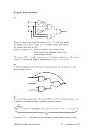
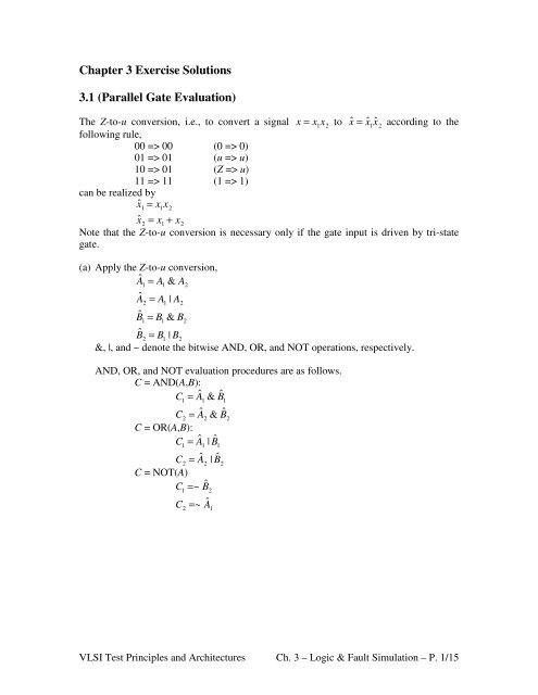
Chapter 3 Exercise Solutions<br />
3.1 (Parallel Gate Evaluation)<br />
The Z-to-u conversion, i.e., to convert a signal x = x 1<br />
x 2<br />
to x ˆ = x ˆ 1<br />
x ˆ 2<br />
according to the<br />
following rule,<br />
00 => 00 (0 => 0)<br />
01 => 01 (u => u)<br />
10 => 01 (Z => u)<br />
11 => 11 (1 => 1)<br />
can be realized by<br />
ˆ x 1<br />
= x 1<br />
x 2<br />
ˆ x 2<br />
= x 1<br />
+ x 2<br />
Note that the Z-to-u conversion is necessary only if the gate input is driven by tri-state<br />
gate.<br />
(a) Apply the Z-to-u conversion,<br />
ˆ A 1<br />
= A 1<br />
& A 2<br />
ˆ A 2<br />
= A 1<br />
| A 2<br />
ˆ B 1<br />
= B 1<br />
& B 2<br />
ˆ B 2<br />
= B 1<br />
| B 2<br />
&, |, and ~ denote the bitwise AND, OR, and NOT operations, respectively.<br />
AND, OR, and NOT evaluation procedures are as follows.<br />
C = AND(A,B):<br />
C 1<br />
= A ˆ<br />
1<br />
& B ˆ<br />
1<br />
C 2<br />
= A ˆ<br />
2<br />
& B ˆ<br />
2<br />
C = OR(A,B):<br />
C 1<br />
= A ˆ<br />
1<br />
| B ˆ<br />
1<br />
C 2<br />
= A ˆ<br />
2<br />
| B ˆ<br />
2<br />
C = NOT(A)<br />
C 1<br />
=~ B ˆ<br />
2<br />
C 2<br />
=~ A ˆ<br />
1<br />
VLSI Test Principles and Architectures Ch. 3 – Logic & Fault Simulation – P. 1/15
(b) Two-to-one multiplexer.<br />
Let A and B be the 0/1 inputs, E the selection input, and O the output.<br />
⎧ A ˆ if E ˆ = 0<br />
⎪<br />
O = ⎨ B ˆ if E ˆ =1<br />
⎪<br />
⎩ u if E ˆ = u<br />
The k-maps are as follows.<br />
O ˆ<br />
1<br />
A ˆ<br />
1<br />
B 1<br />
00 01 11 10<br />
E ˆ ˆ<br />
1<br />
E 2<br />
00 0 0 1 1<br />
01 0 0 0 0<br />
11 0 1 1 0<br />
10 x x x x<br />
O ˆ<br />
2<br />
A ˆ<br />
2<br />
B 2<br />
00 01 11 10<br />
E ˆ ˆ<br />
1<br />
E 2<br />
00 0 0 1 1<br />
01 1 1 1 1<br />
11 0 1 1 0<br />
10 x x x x<br />
It can be derived that<br />
O 1<br />
= A ˆ<br />
1<br />
&( ~ E ˆ<br />
2 )| B ˆ<br />
1<br />
& E ˆ<br />
1<br />
O 2<br />
= ( A ˆ | E ˆ<br />
2 2 )& B ˆ<br />
2<br />
| ~ ˆ<br />
( ( E ) 1<br />
XOR gate<br />
C = XOR( A,B)<br />
The k-maps for C 1<br />
and C 2<br />
are:<br />
C 1<br />
C ˆ<br />
2<br />
A ˆ<br />
1<br />
A 2<br />
00 01 11 10<br />
B ˆ ˆ<br />
1<br />
B 2<br />
00 00 01 11 xx<br />
01 01 01 01 xx<br />
11 11 01 00 xx<br />
10 xx xx xx xx<br />
It can be derived that<br />
C 1<br />
= ( ~ A ˆ<br />
2 )& B ˆ<br />
1<br />
| A ˆ<br />
1<br />
& ~ B ˆ<br />
2<br />
C 2<br />
= A ˆ<br />
2<br />
&( ~ B ˆ<br />
1 )+ ( ~ A ˆ<br />
1 )& ˆ<br />
( )<br />
B 2<br />
VLSI Test Principles and Architectures Ch. 3 – Logic & Fault Simulation – P. 2/15
(c) Tri-state buffer<br />
Let A be the input, E the enabling signal, and O the output.<br />
⎧ A ˆ if E ˆ =1<br />
⎪<br />
O = ⎨ Z if E ˆ = 0<br />
⎪<br />
⎩ u if E ˆ = u<br />
The k-maps for O 1<br />
and O 2<br />
are:<br />
O 1<br />
O ˆ<br />
2<br />
A ˆ<br />
1<br />
A 2<br />
00 01 11 10<br />
E ˆ ˆ<br />
1<br />
E 2<br />
00 10 10 10 xx<br />
01 01 01 01 xx<br />
11 00 01 11 xx<br />
10 xx xx xx xx<br />
It can be derived that<br />
O 1<br />
= ( ~ E ˆ<br />
2 )| A ˆ ˆ<br />
1<br />
E 1<br />
O 2<br />
= ( ~ E ˆ<br />
1 )& E ˆ<br />
2<br />
| A ˆ<br />
2<br />
& E ˆ<br />
2<br />
VLSI Test Principles and Architectures Ch. 3 – Logic & Fault Simulation – P. 3/15
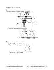
3.2 (Timing Models)<br />
(a) Nominal + Inertial Delays<br />
(b) Rise/Fall Delays<br />
VLSI Test Principles and Architectures Ch. 3 – Logic & Fault Simulation – P. 4/15
(c) Min-Max Delays<br />
VLSI Test Principles and Architectures Ch. 3 – Logic & Fault Simulation – P. 5/15
3.3 (Compiled-Code Simulation)<br />
(a) Levelization<br />
(b) Pseudo code<br />
while(true) do<br />
read(A,B,C);<br />
D = AND(A,B);<br />
E = NOT(B);<br />
F = OR(B,C);<br />
H = AND(D,E);<br />
H = AND(H,F);<br />
H = NOT(H);<br />
J = NOT(F);<br />
L = AND(H,J);<br />
L = NOT(L);<br />
end<br />
VLSI Test Principles and Architectures Ch. 3 – Logic & Fault Simulation – P. 6/15
3.4 (Event-Driven Simulation)<br />
Time L E L A Scheduled Events<br />
0 {(B,0)} {D,E,F} {(D,0,1),(E,1,0.6),(F,1,1)}<br />
0.1 {(A,0)} {D} {(D,0,1.1)}<br />
0.4 {(A,1)} {D} {(D,0,1.4)}<br />
0.5 {(C,0)} {F} {(F,0,1.5)}<br />
0.6 {(E,1)} {H} {(H,0,1.8)}<br />
1 {(D,0),(F,1)} {H} {(H,1,2.2)}<br />
1.1 {(D,0)}<br />
1.4 {(D,0)}<br />
1.5 {(F,0)} {H,J} {(H,1,2.7),(J,1,2.1)}<br />
1.8 {(H,0)} {L} {(L,1,2.8)}<br />
2.1 {(J,1)} {L} {(L,1,3.1)}<br />
2.2 {(H,1)} {L} {(L,0,3.2)}<br />
2.7 {(H,1)}<br />
2.8 {(L,1)}<br />
3.1 {(L,1)}<br />
3.2 {(L,0)}<br />
VLSI Test Principles and Architectures Ch. 3 – Logic & Fault Simulation – P. 7/15
3.5 (Hazard Detection)<br />
To detect static and dynamic hazards, use 8-valued logic.<br />
A = F<br />
B = R<br />
C = F<br />
D = AND(A,B)<br />
= AND(F,R)<br />
= AND({1110,1100,1000},{0001,0011,0111})<br />
= {0000,0010,0110,0100}<br />
= 0*<br />
E = NOT(B)<br />
= NOT(R)<br />
= F<br />
F = OR(B,C)<br />
= OR(R,F)<br />
= OR({0001,0011,0111},{1110,1100,1000})<br />
= {1111,1101,1001,1011}<br />
= 1*<br />
H = NAND(D,E,F)<br />
= NAND(0*,F,1*)<br />
= NAND({0000,0100,0110,0010},{1110,1100,1000},<br />
{1111,1011,1001,1101})<br />
= {1111,1011,1001,1101}<br />
= 1*<br />
J<br />
= NOT(F)<br />
= NOT(1*)<br />
= 0*<br />
L = NAND(H,J)<br />
= NAND(1*,0*)<br />
= 1*<br />
A static 1-hazard may occur at output L.<br />
VLSI Test Principles and Architectures Ch. 3 – Logic & Fault Simulation – P. 8/15
3.6 (Hazard Detection)<br />
Use 8-valued logic.<br />
pattern 1 (10) ==> pattern 2 (01)<br />
a = F<br />
b = R<br />
c = OR(AND(a,b),NOT(b))<br />
= OR(AND(F,R),NOT(R))<br />
= OR(0*,F)<br />
= OR({0000,0100,0110,0010},{1110,1100,1000})<br />
= {1110,1100,1000,1010}<br />
= F*<br />
A dynamic 0-hazard may occur.<br />
pattern 2 (01) ==> pattern 3 (11)<br />
a = R<br />
b = 1<br />
c = OR(AND(a,b),NOT(b))<br />
= OR(AND(R,1),NOT(1))<br />
= OR(R,0)<br />
= R<br />
No static or dynamic hazard.<br />
VLSI Test Principles and Architectures Ch. 3 – Logic & Fault Simulation – P. 9/15
3.7 (Parallel-Pattern Single-Fault Propagation)<br />
PPSFP input internal output<br />
fault P a b D E F c<br />
P1 1 0 0 0 1 1<br />
fault-free P2 0 1 1 0 0 0<br />
P3 1 1 1 1 0 1<br />
P1 1 0 0 0 1 1<br />
α P2 0 1 0 0 0 0<br />
P3 1 1 0 0 0 0<br />
P1 1 0 0 0 1 1<br />
β P2 0 1 1 0 1 1<br />
P3 1 1 1 1 1 1<br />
VLSI Test Principles and Architectures Ch. 3 – Logic & Fault Simulation – P. 10/15
3.8 (Parallel Fault Simulation)<br />
PFS input internal output<br />
Pattern fault a b D E F c<br />
P1<br />
P2<br />
P3<br />
fault-free 1 0 0 0 1 1<br />
α 1 0 0 0 1 1<br />
β 1 0 0 0 1 1<br />
fault-free 0 1 1 0 0 0<br />
α 0 1 0 0 0 0<br />
β 0 1 1 0 1 1<br />
fault-free 1 1 1 1 0 1<br />
α 1 1 0 0 0 0<br />
β 1 1 1 1 1 1<br />
VLSI Test Principles and Architectures Ch. 3 – Logic & Fault Simulation – P. 11/15
3.9 (Deductive Fault Simulation)<br />
The controlling value of a NOR gate is one, and the inversion value is also one. Let S be<br />
the set of inputs that hold the controlling value, and I be the set of all inputs, i.e.,<br />
I = {A, B, C}.<br />
When all inputs hold the non-controlling value (ABC = 000), we have<br />
L D<br />
=<br />
⎛<br />
⎜<br />
⎞<br />
∪ L<br />
⎝ j<br />
⎟ ∪ D/ c ⊕ i<br />
j ∈I ⎠<br />
{ ( )}<br />
= ( L A<br />
∪ L B<br />
∪ L C )∪{ D/0}<br />
When at least one input holds the controlling value, we have<br />
⎛ ⎛<br />
L D<br />
= ⎜<br />
⎞ ⎛ ⎞ ⎞<br />
⎜ ∩ L<br />
⎝ j<br />
⎟ −⎜<br />
∪ L<br />
j ∈S ⎠<br />
j<br />
⎟ ⎟ ∪<br />
⎝ ⎝ j ∈( I −S<br />
{ D/1}<br />
) ⎠ ⎠<br />
For example, if ABC = 110, L D will be<br />
L D<br />
= ( L A<br />
∩ L B )− L C )∪{ D/1}<br />
VLSI Test Principles and Architectures Ch. 3 – Logic & Fault Simulation – P. 12/15
3.10 (Deductive Fault Simulation)<br />
For the purpose of demonstration, we do not perform fault collapsing here. The noncollapsed<br />
fault list is {a/0, a/1, b/0, b/1, D/0, D/1, H/0, H/1, E/0, E/1, F/0, F/1, c/0, c/1}.<br />
VLSI Test Principles and Architectures Ch. 3 – Logic & Fault Simulation – P. 13/15
3.11 (Concurrent Fault Simulation)<br />
VLSI Test Principles and Architectures Ch. 3 – Logic & Fault Simulation – P. 14/15
3.12 (Critical Path Tracing)<br />
VLSI Test Principles and Architectures Ch. 3 – Logic & Fault Simulation – P. 15/15