Training ARM Cortex R5 - Multi Video Designs
Training ARM Cortex R5 - Multi Video Designs
Training ARM Cortex R5 - Multi Video Designs
Create successful ePaper yourself
Turn your PDF publications into a flip-book with our unique Google optimized e-Paper software.
MVD <strong>Training</strong><br />
June-2012<br />
Course description<br />
Ref: 005006A<br />
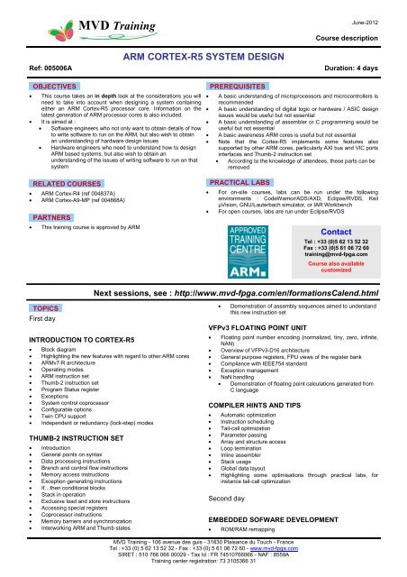
<strong>ARM</strong> CORTEX-<strong>R5</strong> SYSTEM DESIGN<br />
Duration: 4 days<br />
OBJECTIVES<br />
• This course takes an in depth look at the considerations you will<br />
need to take into account when designing a system containing<br />
either an <strong>ARM</strong> <strong>Cortex</strong>-<strong>R5</strong> processor core. Information on the<br />
latest generation of <strong>ARM</strong> processor cores is also included.<br />
• It is aimed at :<br />
• Software engineers who not only want to obtain details of how<br />
to write software to run on the <strong>ARM</strong>, but also wish to obtain<br />
an understanding of hardware design issues<br />
• Hardware engineers who need to understand how to design<br />
<strong>ARM</strong> based systems, but also wish to obtain an<br />
understanding of the issues of writing software to run on that<br />
system<br />
PREREQUISITES<br />
• A basic understanding of microprocessors and microcontrollers is<br />
recommended<br />
• A basic understanding of digital logic or hardware / ASIC design<br />
issues would be useful but not essential<br />
• A basic understanding of assembler or C programming would be<br />
useful but not essential<br />
• A basic awareness <strong>ARM</strong> cores is useful but not essential<br />
• Note that the <strong>Cortex</strong>-<strong>R5</strong> implements some features also<br />
supported by other <strong>ARM</strong> cores, particularly AXI bus and VIC ports<br />
interfaces and Thumb-2 instruction set<br />
• According to the knowledge of attendees, these parts can be<br />
removed<br />
RELATED COURSES<br />
• <strong>ARM</strong> <strong>Cortex</strong>-R4 (ref 004837A)<br />
• <strong>ARM</strong> <strong>Cortex</strong>-A9-MP (ref 004868A)<br />
PARTNERS<br />
• This training course is approved by <strong>ARM</strong><br />
PRACTICAL LABS<br />
• For on-site courses, labs can be run under the following<br />
environments : CodeWarrior/ADS/AXD, Eclipse/RVDS, Keil<br />
µVision, GNU/Lauterbach simulator, or IAR Workbench<br />
• For open courses, labs are run under Eclipse/RVDS<br />
Contact<br />
Tel : +33 (0)5 62 13 52 32<br />
Fax : +33 (0)5 61 06 72 60<br />
training@mvd-fpga.com<br />
Course also available<br />
customized<br />
Next sessions, see : http://www.mvd-fpga.com/en/formationsCalend.html<br />
TOPICS<br />
First day<br />
INTRODUCTION TO CORTEX-<strong>R5</strong><br />
• Block diagram<br />
• Highlighting the new features with regard to other <strong>ARM</strong> cores<br />
• <strong>ARM</strong>v7-R architecture<br />
• Operating modes<br />
• <strong>ARM</strong> instruction set<br />
• Thumb-2 instruction set<br />
• Program Status register<br />
• Exceptions<br />
• System control coprocessor<br />
• Configurable options<br />
• Twin CPU support<br />
• Independent or redundancy (lock-step) modes<br />
THUMB-2 INSTRUCTION SET<br />
• Introduction<br />
• General points on syntax<br />
• Data processing instructions<br />
• Branch and control flow instructions<br />
• Memory access instructions<br />
• Exception generating instructions<br />
• If…then conditional blocks<br />
• Stack in operation<br />
• Exclusive load and store instructions<br />
• Accessing special registers<br />
• Coprocessor instructions<br />
• Memory barriers and synchronization<br />
• Interworking <strong>ARM</strong> and Thumb states<br />
• Demonstration of assembly sequences aimed to understand<br />
this new instruction set<br />
VFPv3 FLOATING POINT UNIT<br />
• Floating point number encoding (normalized, tiny, zero, infinite,<br />
NAN)<br />
• Overview of VFPv3-D16 architecture<br />
• General purpose registers, FPU views of the register bank<br />
• Compliance with IEEE754 standard<br />
• Exception management<br />
• NaN handling<br />
• Demonstration of floating point calculations generated from<br />
C language<br />
COMPILER HINTS AND TIPS<br />
• Automatic optimization<br />
• Instruction scheduling<br />
• Tail-call optimization<br />
• Parameter passing<br />
• Array and structure access<br />
• Loop termination<br />
• Inline assembler<br />
• Stack usage<br />
• Global data layout<br />
• Highlighting some optimisations through practical labs, for<br />
instance tail-call optimization<br />
Second day<br />
EMBEDDED SOFWARE DEVELOPMENT<br />
• ROM/RAM remapping<br />
MVD <strong>Training</strong> - 106 avenue des guis - 31830 Plaisance du Touch - France<br />
Tel : +33 (0) 5 62 13 52 32 - Fax : +33 (0) 5 61 06 72 60 - www.mvd-fpga.com<br />
SIRET : 510 766 066 00029 - Tax Id : FR 74510766066 - NAF : 8559A<br />
<strong>Training</strong> center registration: 73 3105366 31
MVD <strong>Training</strong><br />
• Exception vector table<br />
• Reset handler<br />
• Initialization : stack pointers, code and data areas<br />
• C library initialization<br />
• Scatterloading<br />
• Linker placement rules<br />
• Long branch veneers<br />
• C library functionality<br />
• Placing the stack and heap<br />
INSTRUCTION PIPELINE<br />
• Prefetch unit<br />
• Studying how instructions are processed step by step<br />
• Instruction cycle timing<br />
• Dynamic branch prediction mechanism : global history buffer<br />
• Guidelines for optimal performance<br />
• Data Processing Unit<br />
• Dual issue conditions<br />
• Return stack<br />
• Instruction Memory Barrier<br />
• Prefetch queue flush<br />
• PMU related events<br />
MEMORY TYPES<br />
• Memory types, restriction regarding load / store multiple<br />
• Device and normal memory ordering<br />
• Memory type access restrictions<br />
• Access order<br />
• Memory barriers, self-modifying code<br />
MEMORY PROTECTION UNIT<br />
• Memory protection overview, <strong>ARM</strong> v7 PMSA<br />
• <strong>Cortex</strong>-<strong>R5</strong> MPU and bus faults<br />
• Fault status and address registers<br />
• Region overview, memory type and access control, sub-regions<br />
• Region overlapping<br />
• Setting up the MPU<br />
EXCEPTION MANAGEMENT<br />
• Low Interrupt Latency : abandoning load / store instructions in<br />
progress<br />
• Configuring the state in which exceptions are handled : endian<br />
mode, instruction set<br />
• Configuring the FIQ as non-maskable<br />
• Primecell VICs<br />
• Reducing interrupt latency through automatic vector generation<br />
• VIC basic signal timing<br />
• Connectivity : daisy-chained VIC<br />
• Interrupt priority and masking<br />
• Abort exception, fault handling<br />
• Determining the cause of the fault through CP15 status registers<br />
• Precise vs imprecise faults<br />
Third day<br />
HARDWARE IMPLEMENTATION<br />
• Clock domains, CLKIN, FREECLKIN and PCLKDBG<br />
• Using clock enable to determine the ratio between input clock<br />
and operation clock<br />
• Reset domains, power-on reset and debug reset<br />
• Power control, dynamic power management<br />
• Wait For Interrupt architecture<br />
• Debugging the processor while powered down<br />
AXI PROTOCOL<br />
• Topology : direct connection, multi-master, multi-layer<br />
June-2012<br />
Course description<br />
• PL300 AXI interconnect<br />
• Separate address/control and data phases<br />
• AXI channels, channel handshake<br />
• Support for unaligned data transfers<br />
• Transaction ordering, out of order transaction completion<br />
• Read and write burst timing diagrams<br />
• Atomic transactions<br />
LEVEL 1 MEMORY SYSTEM<br />
• Cache basics : organization, replacement algorithm, write<br />
policies<br />
• Cache organization<br />
• Write with allocate policy<br />
• Debugging when caches are active<br />
• Parity / ECC protection<br />
• Understanding transient cache line load / store : linefill buffers,<br />
eviction buffer<br />
• Accessing the cache RAM from AXI slave interface<br />
• Tightly Coupled Memories, address decoding, enabling on reset<br />
• ECC/parity protection<br />
• Interleaving BTCM accesses initiated by core and AXI DMA<br />
connected to AXI slave interface<br />
• Store buffer, merging data<br />
• L1 caches software read for debug purposes<br />
• PMU related events<br />
Fourth day<br />
LEVEL 2 MEMORY SYSTEM<br />
• AXI master interface, write issuing capability, read issuing<br />
capability<br />
• AXI transaction identifiers<br />
• Controlling an external cache<br />
• Restrictions on AXI transfers<br />
• Determining the number and type of AXI transactions according<br />
to memory attributes and instruction type<br />
• AXI transaction splitting<br />
• AXI slave interface, write issuing capability, read issuing<br />
capability<br />
• Enabling or disabling AXI slave accesses<br />
• Using chip-select to distinguish A-TCM, B-TCM, I-Cache and D-<br />
Cache accesses<br />
• Using the AXI slave interface to perform built-in self tests<br />
• Understanding the error recovery mechanisms<br />
• Exclusive accesses, swap instructions, internal exclusive<br />
monitor, requirement of an external exclusive monitor when<br />
implementing multiple cores<br />
APB - ADVANCED PERIPHERAL BUS<br />
• Second-level address decoding<br />
• Pinout<br />
• Read timing diagram<br />
• Write timing diagram<br />
• APB3.0 new features<br />
DEBUG UNIT<br />
• Performance monitor, event counting<br />
• Related interrupts, event bus<br />
• Coresight specification overview<br />
• CP14 and memory-mapped registers, utilization of an APB slave<br />
interface<br />
• APB port access permissions<br />
• Embedded core debug<br />
• Invasive debug : breakpoints and watchpoints<br />
• Vector catch<br />
• Debug exception<br />
• Debug Communication Channel<br />
• External debug interface<br />
MVD <strong>Training</strong> - 106 avenue des guis - 31830 Plaisance du Touch - France<br />
Tel : +33 (0) 5 62 13 52 32 - Fax : +33 (0) 5 61 06 72 60 - www.mvd-fpga.com<br />
SIRET : 510 766 066 00029 - Tax Id : FR 74510766066 - NAF : 8559A<br />
<strong>Training</strong> center registration: 73 3105366 31
MVD <strong>Training</strong><br />
• Understanding how the Debug unit, the Embedded Trace<br />
Macrocell and the Cross-Triggering Interface interact<br />
June-2012<br />
Course description<br />
• Debugging systems with energy management capabilities<br />
DOCUMENTATION<br />
<strong>Training</strong> manuals will be given to attendees during training in print.<br />
MVD <strong>Training</strong> - 106 avenue des guis - 31830 Plaisance du Touch - France<br />
Tel : +33 (0) 5 62 13 52 32 - Fax : +33 (0) 5 61 06 72 60 - www.mvd-fpga.com<br />
SIRET : 510 766 066 00029 - Tax Id : FR 74510766066 - NAF : 8559A<br />
<strong>Training</strong> center registration: 73 3105366 31


