24LC16B
24LC16B
24LC16B

Create successful ePaper yourself
Turn your PDF publications into a flip-book with our unique Google optimized e-Paper software.
M<br />
16K 2.5V I 2 C Serial EEPROM<br />
<strong>24LC16B</strong><br />
FEATURES<br />
• Single supply with operation down to 2.5V<br />
• Low power CMOS technology<br />
- 1 mA active current typical<br />
- 10 µA standby current typical at 5.5V<br />
- 5 µA standby current typical at 3.0V<br />
• Organized as 8 blocks of 256 bytes (8 x 256 x 8)<br />
• 2-wire serial interface bus, I 2 C compatible<br />
• Schmitt trigger inputs for noise suppression<br />
• Output slope control to eliminate ground bounce<br />
• 100 kHz (E-temp.) and 400 kHz (C/I-temp.)<br />
compatibility<br />
• Self-timed write cycle (including auto-erase)<br />
• Page-write buffer for up to 16 bytes<br />
• 2 ms typical write cycle time for page-write<br />
• Hardware write protect for entire memory<br />
• Can be operated as a serial ROM<br />
• Factory programming (QTP) available<br />
• ESD protection > 4,000V<br />
• 1,000,000 erase/write cycles<br />
• Data retention > 200 years<br />
• 8-pin PDIP, SOIC, TSSOP and MSOP packages<br />
• Available for extended temperature ranges:<br />
- Industrial (I): -40°C to +85°C<br />
- Automotive (E): -40°C to +125°C<br />
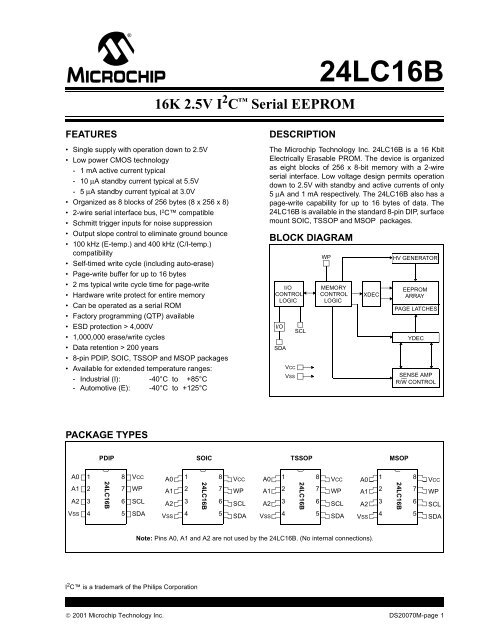
DESCRIPTION<br />
The Microchip Technology Inc. <strong>24LC16B</strong> is a 16 Kbit<br />
Electrically Erasable PROM. The device is organized<br />
as eight blocks of 256 x 8-bit memory with a 2-wire<br />
serial interface. Low voltage design permits operation<br />
down to 2.5V with standby and active currents of only<br />
5 µA and 1 mA respectively. The <strong>24LC16B</strong> also has a<br />
page-write capability for up to 16 bytes of data. The<br />
<strong>24LC16B</strong> is available in the standard 8-pin DIP, surface<br />
mount SOIC, TSSOP and MSOP packages.<br />
BLOCK DIAGRAM<br />
I/O<br />
CONTROL<br />
LOGIC<br />
I/O<br />
SDA<br />
VCC<br />
VSS<br />
SCL<br />
WP<br />
MEMORY<br />
CONTROL<br />
LOGIC<br />
XDEC<br />
HV GENERATOR<br />
EEPROM<br />
ARRAY<br />
PAGE LATCHES<br />
YDEC<br />
SENSE AMP<br />
R/W CONTROL<br />
PACKAGE TYPES<br />
PDIP<br />
SOIC<br />
TSSOP<br />
MSOP<br />
A0<br />
A1<br />
A2<br />
VSS<br />
1<br />
2<br />
3<br />
4<br />
<strong>24LC16B</strong><br />
8<br />
7<br />
6<br />
5<br />
VCC<br />
WP<br />
SCL<br />
SDA<br />
A0<br />
A1<br />
A2<br />
VSS<br />
1<br />
2<br />
3<br />
4<br />
<strong>24LC16B</strong><br />
8<br />
7<br />
6<br />
5<br />
VCC<br />
WP<br />
SCL<br />
SDA<br />
A0<br />
A1<br />
A2<br />
VSS<br />
1<br />
2<br />
3<br />
4<br />
<strong>24LC16B</strong><br />
8<br />
7<br />
6<br />
5<br />
VCC<br />
WP<br />
SCL<br />
SDA<br />
A0<br />
A1<br />
A2<br />
VSS<br />
1<br />
2<br />
3<br />
4<br />
<strong>24LC16B</strong><br />
8<br />
7<br />
6<br />
5<br />
VCC<br />
WP<br />
SCL<br />
SDA<br />
Note: Pins A0, A1 and A2 are not used by the <strong>24LC16B</strong>. (No internal connections).<br />
I 2 C is a trademark of the Philips Corporation<br />
© 2001 Microchip Technology Inc. DS20070M-page 1
<strong>24LC16B</strong><br />
1.0 ELECTRICAL CHARACTERISTICS<br />
Absolute Maximum Ratings†<br />
VCC.............................................................................................................................................................................7.0V<br />
All inputs and outputs w.r.t. VSS ......................................................................................................... -0.3V to VCC +1.0V<br />
Storage temperature ...............................................................................................................................-65°C to +150°C<br />
Ambient temp. with power applied ..........................................................................................................-65°C to +125°C<br />
Soldering temperature of leads (10 seconds) .......................................................................................................+300°C<br />
ESD protection on all pins .....................................................................................................................................................≥ 4KV<br />
† NOTICE: Stresses above those listed under “Maximum ratings” may cause permanent damage to the device.<br />
This is a stress rating only and functional operation of the device at those or any other conditions above those<br />
indicated in the operational listings of this specification is not implied. Exposure to maximum rating conditions<br />
for extended periods may affect device reliability.<br />
1.1 DC Characteristics<br />
DC CHARACTERISTICS<br />
VCC = +2.5V to +5.5V<br />
Industrial (I): TAMB = -40°C to +85°C<br />
Automotive (E): TAMB = -40°C to +125°C<br />
Param.<br />
No.<br />
Sym. Characteristic Min. Max. Units Conditions<br />
D1 VIH WP, SCL and SDA pins — — — —<br />
D2 — High level input voltage .7 VCC — V —<br />
D3 VIL Low level input voltage — .3 VCC V —<br />
D4 VHYS Hysteresis of Schmitt .05 VCC — V (Note)<br />
trigger inputs<br />
D5 VOL Low level output voltage — .40 V IOL = 3.0 mA, VCC = 2.5V<br />
D6 ILI Input leakage current -10 10 µA VIN = .1V to VCC<br />
D7 ILO Output leakage current -10 10 µA VOUT = .1V to VCC<br />
D8 CIN,<br />
COUT<br />
Pin capacitance<br />
(all inputs/outputs)<br />
— 10 pF VCC = 5.0V (Note)<br />
TAMB = 25°C, FCLK = 1 MHz<br />
D9 ICC write Operating current — 3 mA VCC = 5.5V, SCL = 400 kHz<br />
D10 ICC read — 1 mA —<br />
D11 ICCS Standby current —<br />
—<br />
Note:<br />
30<br />
100<br />
This parameter is periodically sampled and not 100% tested.<br />
µΑ<br />
µΑ<br />
VCC = 3.0V, SDA = SCL = VCC<br />
VCC = 5.5V, SDA = SCL = VCC<br />
WP = VSS<br />
DS20070M-page 2<br />
© 2001 Microchip Technology Inc.
<strong>24LC16B</strong><br />
1.2 AC Characteristics<br />
AC CHARACTERISTICS<br />
Param.<br />
No.<br />
1 FCLK Clock frequency —<br />
—<br />
2 THIGH Clock high time 600<br />
4000<br />
3 TLOW Clock low time 1300<br />
4700<br />
VCC = +2.5V to +5.5V<br />
Industrial (I): TAMB = -40°C to +85°C<br />
Automotive (E): TAMB = -40°C to +125°C<br />
Sym. Characteristic. Min. Max. Units Conditions<br />
4 TR SDA and SCL rise time<br />
(Note 1)<br />
—<br />
—<br />
400<br />
100<br />
—<br />
—<br />
—<br />
—<br />
300<br />
1000<br />
5 TF SDA and SCL fall time — 300 ns (Note 1)<br />
6 THD:STA START condition hold<br />
time<br />
7 TSU:STA START condition setup<br />
time<br />
600<br />
4000<br />
600<br />
4700<br />
8 THD:DAT Data input hold time 0 — ns (Note 2)<br />
9 TSU:DAT Data input setup time 100<br />
250<br />
10 TSU:STO STOP condition setup<br />
time<br />
11 TAA Output valid from clock<br />
(Note 2)<br />
12 TBUF Bus free time: Time the<br />
bus must be free before a<br />
new transmission can<br />
start<br />
13 TOF Output fall time from VIH<br />
minimum to VIL maximum<br />
14 TSP Input filter spike<br />
suppression<br />
(SDA and SCL pins)<br />
600<br />
4000<br />
—<br />
—<br />
1300<br />
4700<br />
20+0.1CB<br />
—<br />
—<br />
—<br />
—<br />
—<br />
—<br />
—<br />
—<br />
—<br />
900<br />
3500<br />
—<br />
—<br />
250<br />
250<br />
kHz 2.5V ≤ VCC ≤ 5.5V<br />
2.5V ≤ VCC ≤ 5.5V (E-temp. range)<br />
ns 2.5V ≤ VCC ≤ 5.5V<br />
2.5V ≤ VCC ≤ 5.5V (E-temp. range)<br />
ns 2.5V ≤ VCC ≤ 5.5V<br />
2.5V ≤ VCC ≤ 5.5V (E-temp. range)<br />
ns 2.5V ≤ VCC ≤ 5.5V (Note 1)<br />
2.5V ≤ VCC ≤ 5.5V (E-temp. range)<br />
(Note 1)<br />
ns 2.5V ≤ VCC ≤ 5.5V<br />
2.5V ≤ VCC ≤ 5.5V (E-temp. range)<br />
ns 2.5V ≤ VCC ≤ 5.5V<br />
2.5V ≤ VCC ≤ 5.5V (E-temp. range)<br />
ns 2.5V ≤ VCC ≤ 5.5V<br />
2.5V ≤ VCC ≤ 5.5V (E-temp. range)<br />
ns 2.5V ≤ VCC ≤ 5.5V<br />
2.5V ≤ VCC ≤ 5.5V (E-temp. range)<br />
ns 2.5V ≤ VCC ≤ 5.5V<br />
2.5V ≤ VCC ≤ 5.5V (E-temp. range)<br />
ns 2.5V ≤ VCC ≤ 5.5V<br />
2.5V ≤ VCC ≤ 5.5V (E-temp. range)<br />
ns 2.5V ≤ VCC ≤ 5.5V<br />
2.5V ≤ VCC ≤ 5.5V (E-temp. range)<br />
— 50 ns (Notes 1 and 3)<br />
15 TWC Write cycle time (byte or — 5 ms —<br />
page)<br />
16 — Endurance 1M — cycles 25°C, VCC = 5.0V, Block Mode<br />
(Note 4)<br />
Note 1: Not 100% tested. CB = total capacitance of one bus line in pF.<br />
2: As a transmitter, the device must provide an internal minimum delay time to bridge the undefined region (minimum<br />
300 ns) of the falling edge of SCL to avoid unintended generation of START or STOP conditions.<br />
3: The combined TSP and VHYS specifications are due to new Schmitt trigger inputs which provide improved noise spike<br />
suppression. This eliminates the need for a TI specification for standard operation.<br />
4: This parameter is not tested but ensured by characterization. For endurance estimates in a specific application, please<br />
consult the Total Endurance Model which can be obtained on Microchip’s website: www.microchip.com.<br />
© 2001 Microchip Technology Inc. DS20070M-page 3
<strong>24LC16B</strong><br />
FIGURE 1-1:<br />
BUS TIMING DATA<br />
5<br />
3<br />
2<br />
4<br />
SCL<br />
SDA<br />
IN<br />
14<br />
7<br />
6<br />
8 9 10<br />
11<br />
12<br />
SDA<br />
OUT<br />
FIGURE 1-2:<br />
BUS TIMING START/STOP<br />
D4<br />
SCL<br />
7<br />
6<br />
10<br />
SDA<br />
START<br />
STOP<br />
DS20070M-page 4<br />
© 2001 Microchip Technology Inc.
<strong>24LC16B</strong><br />
2.0 FUNCTIONAL DESCRIPTION<br />
The <strong>24LC16B</strong> supports a bi-directional 2-wire bus and<br />
data transmission protocol. A device that sends data<br />
onto the bus is defined as transmitter, and a device<br />
receiving data as receiver. The bus has to be controlled<br />
by a master device which generates the serial clock<br />
(SCL), controls the bus access and generates the<br />
START and STOP conditions, while the <strong>24LC16B</strong><br />
works as slave. Both master and slave can operate as<br />
transmitter or receiver, but the master device determines<br />
which mode is activated.<br />
3.0 BUS CHARACTERISTICS<br />
The following bus protocol has been defined:<br />
• Data transfer may be initiated only when the bus<br />
is not busy.<br />
• During data transfer, the data line must remain<br />
stable whenever the clock line is HIGH. Changes<br />
in the data line while the clock line is HIGH will be<br />
interpreted as a START or STOP condition.<br />
Accordingly, the following bus conditions have been<br />
defined (Figure 3-1).<br />
3.1 Bus not Busy (A)<br />
Both data and clock lines remain HIGH.<br />
3.2 Start Data Transfer (B)<br />
A HIGH to LOW transition of the SDA line while the<br />
clock (SCL) is HIGH determines a START condition.<br />
All commands must be preceded by a START condition.<br />
3.3 Stop Data Transfer (C)<br />
A LOW to HIGH transition of the SDA line while the<br />
clock (SCL) is HIGH determines a STOP condition. All<br />
operations must be ended with a STOP condition.<br />
3.4 Data Valid (D)<br />
The state of the data line represents valid data when,<br />
after a START condition, the data line is stable for the<br />
duration of the HIGH period of the clock signal.<br />
The data on the line must be changed during the LOW<br />
period of the clock signal. There is one clock pulse per<br />
bit of data.<br />
Each data transfer is initiated with a START condition<br />
and terminated with a STOP condition. The number of<br />
the data bytes transferred between the START and<br />
STOP conditions is determined by the master device<br />
and is theoretically unlimited, although only the last sixteen<br />
will be stored when doing a write operation. When<br />
an overwrite does occur it will replace data in a first-in<br />
first-out (FIFO) fashion.<br />
3.5 Acknowledge<br />
Each receiving device, when addressed, is obliged to<br />
generate an acknowledge after the reception of each<br />
byte. The master device must generate an extra clock<br />
pulse which is associated with this acknowledge bit.<br />
Note:<br />
The <strong>24LC16B</strong> does not generate any<br />
acknowledge bits if an internal programming<br />
cycle is in progress.<br />
The device that acknowledges, has to pull down the<br />
SDA line during the acknowledge clock pulse in such a<br />
way that the SDA line is stable LOW during the HIGH<br />
period of the acknowledge related clock pulse. Of<br />
course, setup and hold times must be taken into<br />
account. During reads, a master must signal an end of<br />
data to the slave by not generating an acknowledge bit<br />
on the last byte that has been clocked out of the slave.<br />
In this case, the slave (<strong>24LC16B</strong>) will leave the data<br />
line HIGH to enable the master to generate the STOP<br />
condition.<br />
FIGURE 3-1:<br />
DATA TRANSFER SEQUENCE ON THE SERIAL BUS<br />
SCL<br />
(A) (B) (D) (D) (C) (A)<br />
SDA<br />
START<br />
CONDITION<br />
ADDRESS OR<br />
ACKNOWLEDGE<br />
VALID<br />
DATA<br />
ALLOWED<br />
TO CHANGE<br />
STOP<br />
CONDITION<br />
© 2001 Microchip Technology Inc. DS20070M-page 5
<strong>24LC16B</strong><br />
3.6 Device Addressing<br />
A control byte is the first byte received following the<br />
start condition from the master device. The control byte<br />
consists of a four bit control code, for the <strong>24LC16B</strong> this<br />
is set as 1010 binary for read and write operations.<br />
The next three bits of the control byte are the block<br />
select bits (B2, B1, B0). They are used by the master<br />
device to select which of the eight 256 word blocks of<br />
memory are to be accessed. These bits are in effect the<br />
three most significant bits of the word address. It<br />
should be noted that the protocol limits the size of the<br />
memory to eight blocks of 256 words, therefore the protocol<br />
can support only one <strong>24LC16B</strong> per system.<br />
The last bit of the control byte defines the operation to<br />
be performed. When set to ‘1’ a read operation is<br />
selected, when set to ‘0’ a write operation is selected.<br />
Following the START condition, the <strong>24LC16B</strong> monitors<br />
the SDA bus checking the device type identifier being<br />
transmitted, upon a 1010 code the slave device outputs<br />
an acknowledge signal on the SDA line. Depending<br />
on the state of the R/W bit, the <strong>24LC16B</strong> will select<br />
a read or write operation.<br />
Operation<br />
Control<br />
Code<br />
Block Select<br />
R/W<br />
Read 1010 Block Address 1<br />
Write 1010 Block Address 0<br />
FIGURE 3-2:<br />
START<br />
CONTROL BYTE<br />
ALLOCATION<br />
1 0 1 0 B2 B1 B0<br />
X = Don’t care<br />
SLAVE ADDRESS<br />
READ/WRITE<br />
R/W<br />
A<br />
DS20070M-page 6<br />
© 2001 Microchip Technology Inc.
<strong>24LC16B</strong><br />
4.0 WRITE OPERATION<br />
4.1 Byte Write<br />
Following the START condition from the master, the<br />
device code (4 bits), the block address (3 bits) and the<br />
R/W bit which is a logic LOW is placed onto the bus by<br />
the master transmitter. This indicates to the addressed<br />
slave receiver that a byte with a word address will follow<br />
after it has generated an acknowledge bit during<br />
the ninth clock cycle. Therefore, the next byte transmitted<br />
by the master is the word address and will be written<br />
into the address pointer of the <strong>24LC16B</strong>. After<br />
receiving another acknowledge signal from the<br />
<strong>24LC16B</strong>, the master device will transmit the data word<br />
to be written into the addressed memory location. The<br />
<strong>24LC16B</strong> acknowledges again and the master generates<br />
a STOP condition. This initiates the internal write<br />
cycle, and during this time the <strong>24LC16B</strong> will not generate<br />
acknowledge signals (Figure 4-1).<br />
4.2 Page Write<br />
The write control byte, word address and the first data<br />
byte are transmitted to the <strong>24LC16B</strong> in the same way<br />
as in a byte write. But instead of generating a STOP<br />
condition the master transmits up to 16 data bytes to<br />
the <strong>24LC16B</strong>, which are temporarily stored in the onchip<br />
page buffer and will be written into the memory<br />
after the master has transmitted a STOP condition.<br />
After the receipt of each word, the four lower order<br />
address pointer bits are internally incremented by ‘1’.<br />
The higher order 7 bits of the word address remains<br />
constant. If the master should transmit more than 16<br />
words prior to generating the STOP condition, the<br />
address counter will roll over and the previously<br />
received data will be overwritten. As with the byte write<br />
operation, once the STOP condition is received an<br />
internal write cycle will begin (Figure 4-2).<br />
Note:<br />
Page write operations are limited to writing<br />
bytes within a single physical page,<br />
regardless of the number of bytes actually<br />
being written. Physical page boundaries<br />
start at addresses that are integer<br />
multiples of the page buffer size (or<br />
‘page size’) and end at addresses that<br />
are integer multiples of [page size - 1]. If<br />
a page write command attempts to write<br />
across a physical page boundary, the<br />
result is that the data wraps around to<br />
the beginning of the current page (overwriting<br />
data previously stored there),<br />
instead of being written to the next page<br />
as might be expected. It is therefore<br />
necessary for the application software to<br />
prevent page write operations that<br />
would attempt to cross a page boundary.<br />
FIGURE 4-1:<br />
BYTE WRITE<br />
BUS ACTIVITY<br />
MASTER<br />
S<br />
T<br />
A<br />
R<br />
T<br />
CONTROL<br />
BYTE<br />
WORD<br />
ADDRESS<br />
DATA<br />
S<br />
T<br />
O<br />
P<br />
SDA LINE<br />
S<br />
P<br />
BUS ACTIVITY<br />
A<br />
C<br />
K<br />
A<br />
C<br />
K<br />
A<br />
C<br />
K<br />
FIGURE 4-2:<br />
PAGE WRITE<br />
BUS ACTIVITY<br />
MASTER<br />
S<br />
T<br />
A<br />
R<br />
T<br />
CONTROL<br />
BYTE<br />
WORD<br />
ADDRESS (n) DATA (n) DATA (n + 1) DATA (n + 15)<br />
S<br />
T<br />
O<br />
P<br />
SDA LINE<br />
BUS ACTIVITY<br />
S<br />
A<br />
C<br />
K<br />
A<br />
C<br />
K<br />
A<br />
C<br />
K<br />
A<br />
C<br />
K<br />
A<br />
C<br />
K<br />
P<br />
© 2001 Microchip Technology Inc. DS20070M-page 7
<strong>24LC16B</strong><br />
5.0 ACKNOWLEDGE POLLING<br />
Since the device will not acknowledge during a write<br />
cycle, this can be used to determine when the cycle is<br />
complete (this feature can be used to maximize bus<br />
throughput). Once the STOP condition for a write command<br />
has been issued from the master, the device initiates<br />
the internally timed write cycle. ACK polling can<br />
be initiated immediately. This involves the master sending<br />
a start condition followed by the control byte for a<br />
write command (R/W = 0). If the device is still busy with<br />
the write cycle, then no ACK will be returned. If the<br />
cycle is complete, then the device will return the ACK<br />
and the master can then proceed with the next read or<br />
write command. See Figure 5-1 for flow diagram.<br />
6.0 WRITE PROTECTION<br />
The <strong>24LC16B</strong> can be used as a serial ROM when the<br />
WP pin is connected to VCC. Programming will be<br />
inhibited and the entire memory will be write-protected.<br />
FIGURE 5-1:<br />
ACKNOWLEDGE POLLING<br />
FLOW<br />
Send<br />
Write Command<br />
Send Stop<br />
Condition to<br />
Initiate Write Cycle<br />
Send Start<br />
Send Control Byte<br />
with R/W = 0<br />
Did Device<br />
Acknowledge<br />
(ACK = 0)<br />
No<br />
Yes<br />
Next<br />
Operation<br />
DS20070M-page 8<br />
© 2001 Microchip Technology Inc.
<strong>24LC16B</strong><br />
7.0 READ OPERATION<br />
Read operations are initiated in the same way as write<br />
operations with the exception that the R/W bit of the<br />
slave address is set to ‘1’. There are three basic types<br />
of read operations: current address read, random read<br />
and sequential read.<br />
7.1 Current Address Read<br />
The <strong>24LC16B</strong> contains an address counter that maintains<br />
the address of the last word accessed, internally<br />
incremented by ‘1’. Therefore, if the previous access<br />
(either a read or write operation) was to address n, the<br />
next current address read operation would access data<br />
from address n + 1. Upon receipt of the slave address<br />
with R/W bit set to ‘1’, the <strong>24LC16B</strong> issues an acknowledge<br />
and transmits the 8-bit data word. The master will<br />
not acknowledge the transfer but does generate a<br />
STOP condition and the <strong>24LC16B</strong> discontinues transmission<br />
(Figure 7-1).<br />
7.2 Random Read<br />
Random read operations allow the master to access<br />
any memory location in a random manner. To perform<br />
this type of read operation, first the word address must<br />
be set. This is done by sending the word address to the<br />
<strong>24LC16B</strong> as part of a write operation. After the word<br />
address is sent, the master generates a START condition<br />
following the acknowledge. This terminates the<br />
write operation, but not before the internal address<br />
pointer is set. Then the master issues the control byte<br />
again but with the R/W bit set to a ‘1’. The <strong>24LC16B</strong> will<br />
then issue an acknowledge and transmits the 8-bit data<br />
word. The master will not acknowledge the transfer but<br />
does generate a STOP condition and the <strong>24LC16B</strong> discontinues<br />
transmission (Figure 7-2).<br />
7.3 Sequential Read<br />
Sequential reads are initiated in the same way as a random<br />
read except that after the <strong>24LC16B</strong> transmits the<br />
first data byte, the master issues an acknowledge as<br />
opposed to a STOP condition in a random read. This<br />
directs the <strong>24LC16B</strong> to transmit the next sequentially<br />
addressed 8-bit word (Figure 7-3).<br />
To provide sequential reads the <strong>24LC16B</strong> contains an<br />
internal address pointer which is incremented by one at<br />
the completion of each operation. This address pointer<br />
allows the entire memory contents to be serially read<br />
during one operation.<br />
7.4 Noise Protection<br />
The <strong>24LC16B</strong> employs a VCC threshold detector circuit<br />
which disables the internal erase/write logic if the VCC<br />
is below 1.5V at nominal conditions.<br />
The SCL and SDA inputs have Schmitt trigger and filter<br />
circuits which suppress noise spikes to assure proper<br />
device operation even on a noisy bus.<br />
FIGURE 7-1:<br />
CURRENT ADDRESS READ<br />
BUS ACTIVITY<br />
MASTER<br />
S<br />
T<br />
A<br />
R<br />
T<br />
CONTROL<br />
BYTE<br />
DATA (n)<br />
S<br />
T<br />
O<br />
P<br />
SDA LINE<br />
S<br />
P<br />
BUS ACTIVITY<br />
A<br />
C<br />
K<br />
N<br />
O<br />
A<br />
C<br />
K<br />
© 2001 Microchip Technology Inc. DS20070M-page 9
<strong>24LC16B</strong><br />
FIGURE 7-2:<br />
RANDOM READ<br />
BUS ACTIVITY<br />
MASTER<br />
S<br />
T<br />
A<br />
R<br />
T<br />
CONTROL<br />
BYTE<br />
WORD<br />
ADDRESS (n)<br />
S<br />
T<br />
A<br />
R<br />
T<br />
CONTROL<br />
BYTE<br />
DATA (n)<br />
S<br />
T<br />
O<br />
P<br />
SDA LINE<br />
BUS ACTIVITY<br />
S<br />
A<br />
C<br />
K<br />
A<br />
C<br />
K<br />
S<br />
A<br />
C<br />
K<br />
N<br />
O<br />
A<br />
C<br />
K<br />
P<br />
FIGURE 7-3:<br />
SEQUENTIAL READ<br />
BUS ACTIVITY<br />
MASTER<br />
CONTROL<br />
BYTE<br />
DATA (n) DATA (n + 1) DATA (n + 2) DATA (n + X)<br />
S<br />
T<br />
O<br />
P<br />
SDA LINE<br />
P<br />
BUS ACTIVITY<br />
A<br />
C<br />
K<br />
A<br />
C<br />
K<br />
A<br />
C<br />
K<br />
A<br />
C<br />
K<br />
N<br />
O<br />
A<br />
C<br />
K<br />
DS20070M-page 10<br />
© 2001 Microchip Technology Inc.
<strong>24LC16B</strong><br />
8.0 PIN DESCRIPTIONS<br />
The descriptions of the pins are listed in Table 8-1.<br />
TABLE 8-1:<br />
PIN FUNCTION TABLE<br />
Name PDIP SOIC TSSOP MSOP Description<br />
A0 1 1 1 1 Not Connected<br />
A1 2 2 2 2 Not Connected<br />
A2 3 3 3 3 Not Connected<br />
VSS 4 4 4 4 Ground<br />
SDA 5 5 5 5 Serial Address/Data I/O<br />
SCL 6 6 6 6 Serial Clock<br />
WP 7 7 7 7 Write Protect Input<br />
VCC 8 8 8 8 +2.5V to 5.5V Power Supply<br />
8.1 Serial Address/Data Input/Output<br />
(SDA)<br />
This is a bi-directional pin used to transfer addresses<br />
and data into and data out of the device. It is an open<br />
drain terminal. Therefore, the SDA bus requires a pullup<br />
resistor to VCC (typical 10 kΩ for 100 kHz, 2 kΩ for<br />
400 kHz).<br />
For normal data transfer SDA is allowed to change only<br />
during SCL LOW. Changes during SCL HIGH are<br />
reserved for indicating the START and STOP conditions.<br />
8.2 Serial Clock (SCL)<br />
This input is used to synchronize the data transfer from<br />
and to the device.<br />
8.3 Write-Protect (WP)<br />
This pin must be connected to either VSS or VCC.<br />
If tied to VSS normal memory operation is enabled<br />
(read/write the entire memory 000-7FF).<br />
If tied to VCC, WRITE operations are inhibited. The<br />
entire memory will be write-protected. Read operations<br />
are not affected.<br />
This feature allows the user to use the <strong>24LC16B</strong> as a<br />
serial ROM when WP is enabled (tied to VCC).<br />
8.4 A0, A1, A2<br />
These pins are not used by the <strong>24LC16B</strong>. They may be<br />
left floating or tied to either VSS or VCC.<br />
© 2001 Microchip Technology Inc. DS20070M-page 11
<strong>24LC16B</strong><br />
9.0 PACKAGING INFORMATION<br />
9.1 Package Marking Information<br />
8-Lead PDIP (300 mil)<br />
XXXXXXXX<br />
XXXXXNNN<br />
YYWW<br />
Example:<br />
<strong>24LC16B</strong><br />
/PNNN<br />
YYWW<br />
8-Lead SOIC (150 mil)<br />
XXXXXXXX<br />
XXXXYYWW<br />
NNN<br />
Example:<br />
<strong>24LC16B</strong><br />
SNYYWW<br />
NNN<br />
8-Lead TSSOP<br />
Example:<br />
XXXX<br />
XYWW<br />
NNN<br />
4L16<br />
YWW<br />
NNN<br />
8-Lead MSOP<br />
XXXXXX<br />
YWWNNN<br />
Example:<br />
4L16I<br />
YWWNNN<br />
Legend: XX...X Customer specific information*<br />
Y Year code (last digit of calendar year)<br />
YY Year code (last 2 digits of calendar year)<br />
WW Week code (week of January 1 is week ‘01’)<br />
NNN Alphanumeric traceability code<br />
Note:<br />
In the event the full Microchip part number cannot be marked on one line, it will<br />
be carried over to the next line thus limiting the number of available characters<br />
for customer specific information.<br />
* Standard PICmicro device marking consists of Microchip part number, year code, week code, and<br />
traceability code. For PICmicro device marking beyond this, certain price adders apply. Please check<br />
with your Microchip Sales Office. For QTP devices, any special marking adders are included in QTP<br />
price.<br />
DS20070M-page 12<br />
© 2001 Microchip Technology Inc.
<strong>24LC16B</strong><br />
8-Lead Plastic Dual In-line (P) – 300 mil (PDIP)<br />
E1<br />
2<br />
D<br />
n<br />
1<br />
α<br />
E<br />
A<br />
A2<br />
c<br />
A1<br />
L<br />
β<br />
eB<br />
B1<br />
B<br />
p<br />
Units INCHES* MILLIMETERS<br />
Dimension Limits MIN NOM MAX MIN NOM MAX<br />
Number of Pins n 8 8<br />
Pitch p .100 2.54<br />
Top to Seating Plane A .140 .155 .170 3.56 3.94 4.32<br />
Molded Package Thickness A2 .115 .130 .145 2.92 3.30 3.68<br />
Base to Seating Plane A1 .015 0.38<br />
Shoulder to Shoulder Width E .300 .313 .325 7.62 7.94 8.26<br />
Molded Package Width E1 .240 .250 .260 6.10 6.35 6.60<br />
Overall Length D .360 .373 .385 9.14 9.46 9.78<br />
Tip to Seating Plane L .125 .130 .135 3.18 3.30 3.43<br />
Lead Thickness c .008 .012 .015 0.20 0.29 0.38<br />
Upper Lead Width B1 .045 .058 .070 1.14 1.46 1.78<br />
Lower Lead Width B .014 .018 .022 0.36 0.46 0.56<br />
Overall Row Spacing § eB .310 .370 .430 7.87 9.40 10.92<br />
Mold Draft Angle Top α 5 10 15 5 10 15<br />
Mold Draft Angle Bottom β 5 10 15 5 10 15<br />
* Controlling Parameter<br />
§ Significant Characteristic<br />
Notes:<br />
Dimensions D and E1 do not include mold flash or protrusions. Mold flash or protrusions shall not exceed<br />
.010” (0.254mm) per side.<br />
JEDEC Equivalent: MS-001<br />
Drawing No. C04-018<br />
© 2001 Microchip Technology Inc. DS20070M-page 13
<strong>24LC16B</strong><br />
8-Lead Plastic Small Outline (SN) – Narrow, 150 mil (SOIC)<br />
E<br />
E1<br />
p<br />
2<br />
D<br />
B<br />
n<br />
1<br />
45×<br />
h<br />
α<br />
c<br />
A<br />
A2<br />
f<br />
β<br />
L<br />
A1<br />
Units<br />
INCHES*<br />
MILLIMETERS<br />
Dimension Limits MIN NOM MAX MIN NOM MAX<br />
Number of Pins<br />
n<br />
8<br />
8<br />
Pitch<br />
p<br />
.050<br />
1.27<br />
Overall Height<br />
A .053 .061 .069 1.35 1.55 1.75<br />
Molded Package Thickness A2 .052 .056 .061 1.32 1.42 1.55<br />
Standoff §<br />
A1 .004 .007 .010 0.10 0.18 0.25<br />
Overall Width<br />
E .228 .237 .244 5.79 6.02 6.20<br />
Molded Package Width<br />
E1 .146 .154 .157 3.71 3.91 3.99<br />
Overall Length<br />
D .189 .193 .197 4.80 4.90 5.00<br />
Chamfer Distance<br />
h .010 .015 .020 0.25 0.38 0.51<br />
Foot Length<br />
L .019 .025 .030 0.48 0.62 0.76<br />
Foot Angle f 0 4 8 0 4 8<br />
Lead Thickness<br />
c .008 .009 .010 0.20 0.23 0.25<br />
Lead Width<br />
B .013 .017 .020 0.33 0.42 0.51<br />
Mold Draft Angle Top<br />
α<br />
0 12 15<br />
0 12 15<br />
Mold Draft Angle Bottom<br />
β<br />
0 12 15<br />
0 12 15<br />
* Controlling Parameter<br />
§ Significant Characteristic<br />
Notes:<br />
Dimensions D and E1 do not include mold flash or protrusions. Mold flash or protrusions shall not exceed<br />
.010” (0.254mm) per side.<br />
JEDEC Equivalent: MS-012<br />
Drawing No. C04-057<br />
DS20070M-page 14<br />
© 2001 Microchip Technology Inc.
<strong>24LC16B</strong><br />
8-Lead Plastic Thin Shrink Small Outline (ST) – 4.4 mm (TSSOP)<br />
E<br />
E1<br />
p<br />
2<br />
D<br />
B<br />
n<br />
1<br />
A<br />
α<br />
c<br />
f<br />
A1<br />
A2<br />
β<br />
L<br />
Units<br />
INCHES<br />
MILLIMETERS*<br />
Dimension Limits MIN NOM MAX MIN NOM MAX<br />
Number of Pins<br />
n<br />
8<br />
8<br />
Pitch<br />
p<br />
.026<br />
0.65<br />
Overall Height<br />
A<br />
.043<br />
1.10<br />
Molded Package Thickness A2 .033 .035 .037 0.85 0.90 0.95<br />
Standoff §<br />
A1 .002 .004 .006 0.05 0.10 0.15<br />
Overall Width<br />
E .246 .251 .256 6.25 6.38 6.50<br />
Molded Package Width<br />
E1 .169 .173 .177 4.30 4.40 4.50<br />
Molded Package Length<br />
D .114 .118 .122 2.90 3.00 3.10<br />
Foot Length<br />
L .020 .024 .028 0.50 0.60 0.70<br />
Foot Angle f 0 4 8 0 4 8<br />
Lead Thickness<br />
c .004 .006 .008 0.09 0.15 0.20<br />
Lead Width<br />
B .007 .010 .012 0.19 0.25 0.30<br />
Mold Draft Angle Top<br />
α<br />
0<br />
5 10<br />
0<br />
5 10<br />
Mold Draft Angle Bottom<br />
β<br />
0<br />
5 10<br />
0<br />
5 10<br />
* Controlling Parameter<br />
§ Significant Characteristic<br />
Notes:<br />
Dimensions D and E1 do not include mold flash or protrusions. Mold flash or protrusions shall not exceed<br />
.005” (0.127mm) per side.<br />
JEDEC Equivalent: MO-153<br />
Drawing No. C04-086<br />
© 2001 Microchip Technology Inc. DS20070M-page 15
<strong>24LC16B</strong><br />
8-Lead Plastic Micro Small Outline Package (MSOP)<br />
n 1<br />
2<br />
α<br />
φ<br />
β<br />
Units<br />
INCHES<br />
MILLIMETERS*<br />
Dimension Limits MIN NOM MAX MIN NOM<br />
Number of Pins<br />
n<br />
8<br />
8<br />
Pitch<br />
p<br />
.026 TYP.<br />
0.65 TYP.<br />
Overall Height<br />
A<br />
.043<br />
Molded Package Thickness A2 .032 .034 .036 0.81 0.86<br />
Standoff<br />
A1 .002<br />
.006 0.05<br />
Overall Width<br />
E<br />
.193 TYP.<br />
4.90 TYP.<br />
Molded Package Width<br />
E1 .116 .118 .120 2.95 3.00<br />
Overall Length<br />
D .116 .118 .120 2.95 3.00<br />
Foot Length<br />
L .016 .022 .028 0.40 0.55<br />
Footprint (Reference)<br />
F .035 .037 .039 0.90 0.95<br />
Foot Angle<br />
Lead Thickness<br />
Lead Width<br />
φ<br />
c<br />
B<br />
0<br />
.005<br />
.010<br />
.006<br />
.012<br />
6<br />
.007<br />
.016<br />
0<br />
0.13<br />
0.25<br />
0.15<br />
0.30<br />
Mold Draft Angle Top<br />
Mold Draft Angle Bottom<br />
α<br />
β<br />
7<br />
7<br />
7<br />
7<br />
*Controlling Parameter<br />
Notes:<br />
Dimensions D and E1 do not include mold flash or protrusions. Mold flash or protrusions shall not<br />
exceed .010" (0.254mm) per side.<br />
MAX<br />
1.10<br />
0.91<br />
0.15<br />
3.05<br />
3.05<br />
0.70<br />
1.00<br />
6<br />
0.18<br />
0.40<br />
DS20070M-page 16<br />
© 2001 Microchip Technology Inc.
<strong>24LC16B</strong><br />
ON-LINE SUPPORT<br />
Microchip provides on-line support on the Microchip<br />
World Wide Web (WWW) site.<br />
The web site is used by Microchip as a means to make<br />
files and information easily available to customers. To<br />
view the site, the user must have access to the Internet<br />
and a web browser, such as Netscape ® or Microsoft ®<br />
Explorer. Files are also available for FTP download<br />
from our FTP site.<br />
Connecting to the Microchip Internet Web Site<br />
The Microchip web site is available by using your<br />
favorite Internet browser to attach to:<br />
www.microchip.com<br />
The file transfer site is available by using an FTP service<br />
to connect to:<br />
ftp://ftp.microchip.com<br />
The web site and file transfer site provide a variety of<br />
services. Users may download files for the latest<br />
Development Tools, Data Sheets, Application Notes,<br />
User’s Guides, Articles and Sample Programs. A variety<br />
of Microchip specific business information is also<br />
available, including listings of Microchip sales offices,<br />
distributors and factory representatives. Other data<br />
available for consideration is:<br />
• Latest Microchip Press Releases<br />
• Technical Support Section with Frequently Asked<br />
Questions<br />
• Design Tips<br />
• Device Errata<br />
• Job Postings<br />
• Microchip Consultant Program Member Listing<br />
• Links to other useful web sites related to<br />
Microchip Products<br />
• Conferences for products, Development Systems,<br />
technical information and more<br />
• Listing of seminars and events<br />
Systems Information and Upgrade Hot Line<br />
The Systems Information and Upgrade Line provides<br />
system users a listing of the latest versions of all of<br />
Microchip's development systems software products.<br />
Plus, this line provides information on how customers<br />
can receive any currently available upgrade kits.The<br />
Hot Line Numbers are:<br />
1-800-755-2345 for U.S. and most of Canada, and<br />
1-480-792-7302 for the rest of the world.<br />
© 2001 Microchip Technology Inc. DS20070M-page 17
<strong>24LC16B</strong><br />
READER RESPONSE<br />
It is our intention to provide you with the best documentation possible to ensure successful use of your Microchip product.<br />
If you wish to provide your comments on organization, clarity, subject matter, and ways in which our documentation<br />
can better serve you, please FAX your comments to the Technical Publications Manager at (480) 792-7578.<br />
Please list the following information, and use this outline to provide us with your comments about this Data Sheet.<br />
To: Technical Publications Manager<br />
Total Pages Sent<br />
RE: Reader Response<br />
From: Name<br />
Company<br />
Address<br />
City / State / ZIP / Country<br />
Telephone: (_______) _________ - _________<br />
Application (optional):<br />
Would you like a reply Y N<br />
FAX: (______) _________ - _________<br />
Device:<br />
<strong>24LC16B</strong><br />
Literature Number:<br />
DS20070M<br />
Questions:<br />
1. What are the best features of this document<br />
2. How does this document meet your hardware and software development needs<br />
3. Do you find the organization of this data sheet easy to follow If not, why<br />
4. What additions to the data sheet do you think would enhance the structure and subject<br />
5. What deletions from the data sheet could be made without affecting the overall usefulness<br />
6. Is there any incorrect or misleading information (what and where)<br />
7. How would you improve this document<br />
8. How would you improve our software, systems, and silicon products<br />
DS20070M-page 18<br />
© 2001 Microchip Technology Inc.
<strong>24LC16B</strong><br />
NOTES:<br />
© 2001 Microchip Technology Inc. DS20070M-page 19
<strong>24LC16B</strong><br />
NOTES:<br />
DS20070M-page 20<br />
© 2001 Microchip Technology Inc.
<strong>24LC16B</strong><br />
NOTES:<br />
© 2001 Microchip Technology Inc. DS20070M-page 21
<strong>24LC16B</strong><br />
PRODUCT IDENTIFICATION SYSTEM<br />
To order or obtain information, e.g., on pricing or delivery, refer to the factory or the listed sales office.<br />
PART NO. X /XX<br />
Device<br />
Temperature<br />
Range<br />
Package<br />
Device: <strong>24LC16B</strong>: = 16 Kbit I 2 C Serial EEPROM<br />
<strong>24LC16B</strong>T: = 16 Kbit I 2 C Serial EEPROM<br />
(Tape and Reel)<br />
Temperature<br />
Range:<br />
I<br />
E<br />
=-40°C to +85°C<br />
=-40°C to +125°C<br />
Package: P = Plastic DIP (300 mil body), 8-lead<br />
SN = Plastic SOIC (150 mil body), 8-lead<br />
ST = Plastic TSSOP (4.4 mm), 8-lead<br />
MS = Plastic Micro Small Outline (MSOP), 8-lead<br />
Examples:<br />
a) <strong>24LC16B</strong>-E/P: Extended Temp.,<br />
PDIP package<br />
b) <strong>24LC16B</strong>-E/SN: Extended Temp.,<br />
SOIC package<br />
c) <strong>24LC16B</strong>T-E/SN: Tape and Reel,<br />
Extended Temp., SOIC package<br />
d) <strong>24LC16B</strong>-I/P: Industrial Temp.,<br />
PDIP package<br />
e) <strong>24LC16B</strong>-I/SN: Industrial Temp.,<br />
SOIC package<br />
f) <strong>24LC16B</strong>T-I/SN: Tape and Reel,<br />
Industrial Temp., SOIC package<br />
g) <strong>24LC16B</strong>-I/ST: Industrial Temp.,<br />
TSSOP package<br />
h) <strong>24LC16B</strong>T-I/ST: Tape and Reel,<br />
Industrial Temp., TSSOP package<br />
Sales and Support<br />
Data Sheets<br />
Products supported by a preliminary Data Sheet may have an errata sheet describing minor operational differences<br />
and recommended workarounds. To determine if an errata sheet exists for a particular device, please contact one of<br />
the following:<br />
1. Your local Microchip sales office<br />
2. The Microchip Corporate Literature Center U.S. Fax: (480) 792-7277<br />
3. The Microchip Worldwide Site (www.microchip.com)<br />
Please specify which device, revision of silicon and Data Sheet (include Literature #) you are using.<br />
New Customer Notification System<br />
Register on our web site (www.microchip.com/cn) to receive the most current information on our products.<br />
DS20070M-page 22<br />
© 2001 Microchip Technology Inc.
<strong>24LC16B</strong><br />
“All rights reserved. Copyright © 2001, Microchip<br />
Technology Incorporated, USA. Information contained<br />
in this publication regarding device applications and the<br />
like is intended through suggestion only and may be<br />
superseded by updates. No representation or warranty<br />
is given and no liability is assumed by Microchip<br />
Technology Incorporated with respect to the accuracy<br />
or use of such information, or infringement of patents or<br />
other intellectual property rights arising from such use<br />
or otherwise. Use of Microchip’s products as critical<br />
components in life support systems is not authorized<br />
except with express written approval by Microchip. No<br />
licenses are conveyed, implicitly or otherwise, under<br />
any intellectual property rights. The Microchip logo and<br />
name are registered trademarks of Microchip<br />
Technology Inc. in the U.S.A. and other countries. All<br />
rights reserved. All other trademarks mentioned herein<br />
are the property of their respective companies. No<br />
licenses are conveyed, implicitly or otherwise, under<br />
any intellectual property rights.”<br />
Trademarks<br />
The Microchip name, logo, PIC, PICmicro,<br />
PICMASTER, PICSTART, PRO MATE, KEELOQ,<br />
SEEVAL, MPLAB and The Embedded Control<br />
Solutions Company are registered trademarks of<br />
Microchip Technology Incorporated in the U.S.A. and<br />
other countries.<br />
Total Endurance, ICSP, In-Circuit Serial Programming,<br />
FilterLab, MXDEV, microID, FlexROM, fuzzyLAB,<br />
MPASM, MPLINK, MPLIB, PICDEM, ICEPIC,<br />
Migratable Memory, FanSense, ECONOMONITOR,<br />
Select Mode and microPort are trademarks of<br />
Microchip Technology Incorporated in the U.S.A.<br />
Serialized Quick Term Programming (SQTP) is a<br />
service mark of Microchip Technology Incorporated in<br />
the U.S.A.<br />
All other trademarks mentioned herein are property of<br />
their respective companies.<br />
© 2001, Microchip Technology Incorporated, Printed in<br />
the U.S.A., All Rights Reserved.<br />
Microchip received QS-9000 quality system<br />
certification for its worldwide headquarters,<br />
design and wafer fabrication facilities in<br />
Chandler and Tempe, Arizona in July 1999. The<br />
Company’s quality system processes and<br />
procedures are QS-9000 compliant for its<br />
PICmicro ® 8-bit MCUs, KEELOQ ® code hopping<br />
devices, Serial EEPROMs and microperipheral<br />
products. In addition, Microchip’s quality<br />
system for the design and manufacture of<br />
development systems is ISO 9001 certified.<br />
© 2001 Microchip Technology Inc. DS20070M-page 23
M<br />
WORLDWIDE SALES AND SERVICE<br />
AMERICAS<br />
Corporate Office<br />
2355 West Chandler Blvd.<br />
Chandler, AZ 85224-6199<br />
Tel: 480-792-7200 Fax: 480-792-7277<br />
Technical Support: 480-792-7627<br />
Web Address: http://www.microchip.com<br />
Rocky Mountain<br />
2355 West Chandler Blvd.<br />
Chandler, AZ 85224-6199<br />
Tel: 480-792-7966 Fax: 480-792-7456<br />
Atlanta<br />
500 Sugar Mill Road, Suite 200B<br />
Atlanta, GA 30350<br />
Tel: 770-640-0034 Fax: 770-640-0307<br />
Austin<br />
Analog Product Sales<br />
8303 MoPac Expressway North<br />
Suite A-201<br />
Austin, TX 78759<br />
Tel: 512-345-2030 Fax: 512-345-6085<br />
Boston<br />
2 Lan Drive, Suite 120<br />
Westford, MA 01886<br />
Tel: 978-692-3848 Fax: 978-692-3821<br />
Boston<br />
Analog Product Sales<br />
Unit A-8-1 Millbrook Tarry Condominium<br />
97 Lowell Road<br />
Concord, MA 01742<br />
Tel: 978-371-6400 Fax: 978-371-0050<br />
Chicago<br />
333 Pierce Road, Suite 180<br />
Itasca, IL 60143<br />
Tel: 630-285-0071 Fax: 630-285-0075<br />
Dallas<br />
4570 Westgrove Drive, Suite 160<br />
Addison, TX 75001<br />
Tel: 972-818-7423 Fax: 972-818-2924<br />
Dayton<br />
Two Prestige Place, Suite 130<br />
Miamisburg, OH 45342<br />
Tel: 937-291-1654 Fax: 937-291-9175<br />
Detroit<br />
Tri-Atria Office Building<br />
32255 Northwestern Highway, Suite 190<br />
Farmington Hills, MI 48334<br />
Tel: 248-538-2250 Fax: 248-538-2260<br />
Los Angeles<br />
18201 Von Karman, Suite 1090<br />
Irvine, CA 92612<br />
Tel: 949-263-1888 Fax: 949-263-1338<br />
Mountain View<br />
Analog Product Sales<br />
1300 Terra Bella Avenue<br />
Mountain View, CA 94043-1836<br />
Tel: 650-968-9241 Fax: 650-967-1590<br />
New York<br />
150 Motor Parkway, Suite 202<br />
Hauppauge, NY 11788<br />
Tel: 631-273-5305 Fax: 631-273-5335<br />
San Jose<br />
Microchip Technology Inc.<br />
2107 North First Street, Suite 590<br />
San Jose, CA 95131<br />
Tel: 408-436-7950 Fax: 408-436-7955<br />
Toronto<br />
6285 Northam Drive, Suite 108<br />
Mississauga, Ontario L4V 1X5, Canada<br />
Tel: 905-673-0699 Fax: 905-673-6509<br />
ASIA/PACIFIC<br />
Australia<br />
Microchip Technology Australia Pty Ltd<br />
Suite 22, 41 Rawson Street<br />
Epping 2121, NSW<br />
Australia<br />
Tel: 61-2-9868-6733 Fax: 61-2-9868-6755<br />
China - Beijing<br />
Microchip Technology Beijing Office<br />
Unit 915<br />
New China Hong Kong Manhattan Bldg.<br />
No. 6 Chaoyangmen Beidajie<br />
Beijing, 100027, No. China<br />
Tel: 86-10-85282100 Fax: 86-10-85282104<br />
China - Shanghai<br />
Microchip Technology Shanghai Office<br />
Room 701, Bldg. B<br />
Far East International Plaza<br />
No. 317 Xian Xia Road<br />
Shanghai, 200051<br />
Tel: 86-21-6275-5700 Fax: 86-21-6275-5060<br />
Hong Kong<br />
Microchip Asia Pacific<br />
RM 2101, Tower 2, Metroplaza<br />
223 Hing Fong Road<br />
Kwai Fong, N.T., Hong Kong<br />
Tel: 852-2401-1200 Fax: 852-2401-3431<br />
India<br />
Microchip Technology Inc.<br />
India Liaison Office<br />
Divyasree Chambers<br />
1 Floor, Wing A (A3/A4)<br />
No. 11, O’Shaugnessey Road<br />
Bangalore, 560 025, India<br />
Tel: 91-80-2290061 Fax: 91-80-2290062<br />
Japan<br />
Microchip Technology Intl. Inc.<br />
Benex S-1 6F<br />
3-18-20, Shinyokohama<br />
Kohoku-Ku, Yokohama-shi<br />
Kanagawa, 222-0033, Japan<br />
Tel: 81-45-471- 6166 Fax: 81-45-471-6122<br />
ASIA/PACIFIC (continued)<br />
Korea<br />
Microchip Technology Korea<br />
168-1, Youngbo Bldg. 3 Floor<br />
Samsung-Dong, Kangnam-Ku<br />
Seoul, Korea<br />
Tel: 82-2-554-7200 Fax: 82-2-558-5934<br />
Singapore<br />
Microchip Technology Singapore Pte Ltd.<br />
200 Middle Road<br />
#07-02 Prime Centre<br />
Singapore, 188980<br />
Tel: 65-334-8870 Fax: 65-334-8850<br />
Taiwan<br />
Microchip Technology Taiwan<br />
11F-3, No. 207<br />
Tung Hua North Road<br />
Taipei, 105, Taiwan<br />
Tel: 886-2-2717-7175 Fax: 886-2-2545-0139<br />
EUROPE<br />
Denmark<br />
Microchip Technology Denmark ApS<br />
Regus Business Centre<br />
Lautrup hoj 1-3<br />
Ballerup DK-2750 Denmark<br />
Tel: 45 4420 9895 Fax: 45 4420 9910<br />
France<br />
Arizona Microchip Technology SARL<br />
Parc d’Activite du Moulin de Massy<br />
43 Rue du Saule Trapu<br />
Batiment A - ler Etage<br />
91300 Massy, France<br />
Tel: 33-1-69-53-63-20 Fax: 33-1-69-30-90-79<br />
Germany<br />
Arizona Microchip Technology GmbH<br />
Gustav-Heinemann Ring 125<br />
D-81739 Munich, Germany<br />
Tel: 49-89-627-144 0 Fax: 49-89-627-144-44<br />
Germany<br />
Analog Product Sales<br />
Lochhamer Strasse 13<br />
D-82152 Martinsried, Germany<br />
Tel: 49-89-895650-0 Fax: 49-89-895650-22<br />
Italy<br />
Arizona Microchip Technology SRL<br />
Centro Direzionale Colleoni<br />
Palazzo Taurus 1 V. Le Colleoni 1<br />
20041 Agrate Brianza<br />
Milan, Italy<br />
Tel: 39-039-65791-1 Fax: 39-039-6899883<br />
United Kingdom<br />
Arizona Microchip Technology Ltd.<br />
505 Eskdale Road<br />
Winnersh Triangle<br />
Wokingham<br />
Berkshire, England RG41 5TU<br />
Tel: 44 118 921 5869 Fax: 44-118 921-5820<br />
01/30/01<br />
All rights reserved. © 2001 Microchip Technology Incorporated. Printed in the USA. 5/01 Printed on recycled paper.<br />
Information contained in this publication regarding device applications and the like is intended through suggestion only and may be superseded by<br />
updates. It is your responsibility to ensure that your application meets with your specifications. No representation or warranty is given and no liability is<br />
assumed by Microchip Technology Incorporated with respect to the accuracy or use of such information, or infringement of patents or other intellectual<br />
property rights arising from such use or otherwise. Use of Microchip’s products as critical components in life support systems is not authorized except with<br />
express written approval by Microchip. No licenses are conveyed, implicitly or otherwise, except as maybe explicitly expressed herein, under any intellectual<br />
property rights. The Microchip logo and name are registered trademarks of Microchip Technology Inc. in the U.S.A. and other countries. All rights<br />
reserved. All other trademarks mentioned herein are the property of their respective companies.<br />
DS20070M-page 24<br />
© 2001 Microchip Technology Inc.