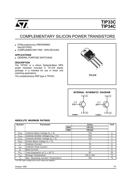
COMPLEMENTARY SILICON POWER TRANSISTORS
COMPLEMENTARY SILICON POWER TRANSISTORS
COMPLEMENTARY SILICON POWER TRANSISTORS

You also want an ePaper? Increase the reach of your titles
YUMPU automatically turns print PDFs into web optimized ePapers that Google loves.
®<br />
TIP33C<br />
TIP34C<br />
<strong>COMPLEMENTARY</strong> <strong>SILICON</strong> <strong>POWER</strong> <strong>TRANSISTORS</strong><br />
■<br />
■<br />
STMicroelectronics PREFERRED<br />
SALESTYPES<br />
<strong>COMPLEMENTARY</strong> PNP - NPN DEVICES<br />
APPLICATIONS<br />
■ GENERAL PURPOSE SWITCHING<br />
DESCRIPTION<br />
The TIP33C is a silicon Epitaxial-Base NPN<br />
power transistor mounted in TO-218 plastic<br />
package. It is intented for use in linear and<br />
switching applications.<br />
The complementary PNP type is TIP34C.<br />
TO-218<br />
1<br />
2<br />
3<br />
INTERNAL SCHEMATIC DIAGRAM<br />
ABSOLUTE MAXIMUM RATINGS<br />
Symbol Parameter Value Unit<br />
NPN<br />
TIP33C<br />
PNP<br />
TIP34C<br />
V CBO Collector-Base Voltage (I E = 0) 140 V<br />
V CES Collector-Emitter Voltage (V BE = 0) 140 V<br />
V CEO Collector-Emitter Voltage (I B = 0) 100 V<br />
V EBO Emitter-Base Voltage (I C = 0) 7 V<br />
I C Collector Current 10 A<br />
I CM Collector Peak Current 12 A<br />
I B Base Current 3 A<br />
P tot Total Dissipation at T c ≤ 25 o C 80 W<br />
T stg Storage Temperature -65 to 150<br />
o C<br />
T j Max. Operating Junction Temperature 150<br />
o C<br />
For PNP types voltage and current values are negative.<br />
October 1999<br />
1/4
TIP33C / TIP34C<br />
THERMAL DATA<br />
R thj-case Thermal Resistance Junction-case Max 1.56<br />
o C/W<br />
ELECTRICAL CHARACTERISTICS (Tcase = 25 o C unless otherwise specified)<br />
Symbol Parameter Test Conditions Min. Typ. Max. Unit<br />
I CES Collector Cut-off V CE = 140 V 400 µA<br />
Current (V BE = 0)<br />
I CEO Collector Cut-off V CE = 60 V 0.7 mA<br />
Current (I B = 0)<br />
I EBO Emitter Cut-off Current<br />
(I C = 0)<br />
V EB = 5 V 1 mA<br />
V CEO(sus)∗<br />
Collector-Emitter<br />
Sustaining Voltage<br />
(I B = 0)<br />
V CE(sat) ∗ Collector-Emitter I C = 3 A<br />
I B = 0.3 A<br />
Saturation Voltage I C = 10 A<br />
I B = 2.5 A<br />
V BE(on) ∗ Base-Emitter Voltage I C = 3 A V CE = 4 V<br />
I C = 10 A<br />
V CE = 4 V<br />
h FE ∗ DC Current Gain I C = 1 A V CE = 4 V<br />
I C = 3 A<br />
V CE = 4 V<br />
h fe Small Signal Current I C = 0.5 A V CE = 10 V<br />
Gain<br />
f = 1 KHz<br />
f T Transition frequency I C = 0.5 A V CE = 10 V<br />
f = 1 MHz<br />
t on<br />
t s<br />
RESISTIVE LOAD<br />
Turn-on Time<br />
Storage Time<br />
Fall Time<br />
t f<br />
∗ Pulsed: Pulse duration = 300 µs, duty cycle 1.5 %<br />
I C = 30 mA 100 V<br />
VCC = 30V<br />
V BB = - 6 V<br />
t p = 20 µs<br />
I C = 6 A<br />
I B1 = - I B2 = 0.6 A<br />
1<br />
4<br />
1.6<br />
3<br />
40<br />
20 100<br />
20<br />
V<br />
V<br />
V<br />
V<br />
3 MHz<br />
0.6<br />
0.4<br />
1<br />
µs<br />
µs<br />
µs<br />
2/4
TIP33C / TIP34C<br />
TO-218 (SOT-93) MECHANICAL DATA<br />
DIM.<br />
mm<br />
inch<br />
MIN. TYP. MAX. MIN. TYP. MAX.<br />
A 4.7 4.9 0.185 0.193<br />
C 1.17 1.37 0.046 0.054<br />
D 2.5 0.098<br />
E 0.5 0.78 0.019 0.030<br />
F 1.1 1.3 0.043 0.051<br />
G 10.8 11.1 0.425 0.437<br />
H 14.7 15.2 0.578 0.598<br />
L2 – 16.2 – 0.637<br />
L3 18 0.708<br />
L5 3.95 4.15 0.155 0.163<br />
L6 31 1.220<br />
R – 12.2 – 0.480<br />
Ø 4 4.1 0.157 0.161<br />
A<br />
E<br />
C<br />
D<br />
L5<br />
L3<br />
L2<br />
L6<br />
H<br />
G<br />
¯<br />
R<br />
1 2 3<br />
F<br />
P025A<br />
3/4
TIP33C / TIP34C<br />
Information furnished is believed to be accurate and reliable. However, STMicroelectronics assumes no responsibility for the consequences<br />
of use of such information nor for any infringement of patents or other rights of third parties which may result from its use. No license is<br />
granted by implication or otherwise under any patent or patent rights of STMicroelectronics. Specification mentioned in this publication are<br />
subject to change without notice. This publication supersedes and replaces all information previously supplied. STMicroelectronics products<br />
are not authorized for use as critical components in life support devices or systems without express written approval of STMicroelectronics.<br />
The ST logo is a trademark of STMicroelectronics<br />
© 1999 STMicroelectronics – Printed in Italy – All Rights Reserved<br />
STMicroelectronics GROUP OF COMPANIES<br />
Australia - Brazil - China - Finland - France - Germany - Hong Kong - India - Italy - Japan - Malaysia - Malta - Morocco -<br />
Singapore - Spain - Sweden - Switzerland - United Kingdom - U.S.A.<br />
4/4<br />
http://www.st.com<br />
.