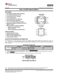
INA138 INA168 - Datasheet Catalog
INA138 INA168 - Datasheet Catalog
INA138 INA168 - Datasheet Catalog

Create successful ePaper yourself
Turn your PDF publications into a flip-book with our unique Google optimized e-Paper software.
®<br />
<strong>INA138</strong><br />
<strong>INA168</strong><br />
For most current data sheet and other product<br />
information, visit www.burr-brown.com<br />
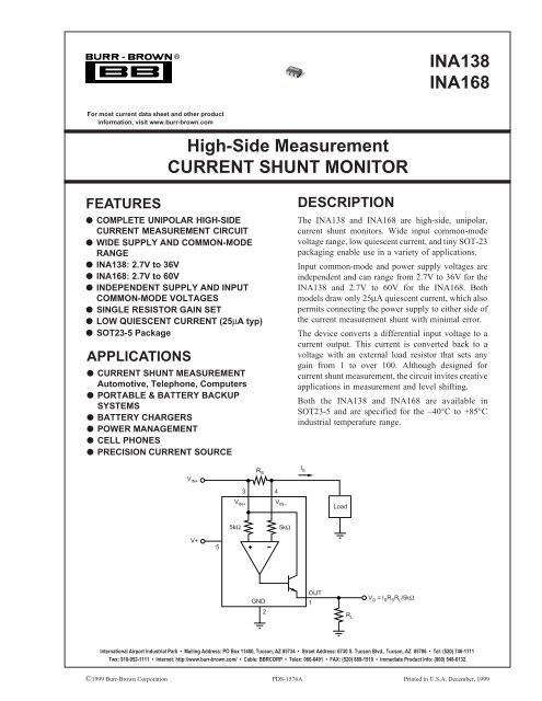
High-Side Measurement<br />
CURRENT SHUNT MONITOR<br />
FEATURES<br />
● COMPLETE UNIPOLAR HIGH-SIDE<br />
CURRENT MEASUREMENT CIRCUIT<br />
● WIDE SUPPLY AND COMMON-MODE<br />
RANGE<br />
● <strong>INA138</strong>: 2.7V to 36V<br />
● <strong>INA168</strong>: 2.7V to 60V<br />
● INDEPENDENT SUPPLY AND INPUT<br />
COMMON-MODE VOLTAGES<br />
● SINGLE RESISTOR GAIN SET<br />
● LOW QUIESCENT CURRENT (25µA typ)<br />
● SOT23-5 Package<br />
APPLICATIONS<br />
● CURRENT SHUNT MEASUREMENT<br />
Automotive, Telephone, Computers<br />
● PORTABLE & BATTERY BACKUP<br />
SYSTEMS<br />
● BATTERY CHARGERS<br />
● POWER MANAGEMENT<br />
● CELL PHONES<br />
● PRECISION CURRENT SOURCE<br />
DESCRIPTION<br />
The <strong>INA138</strong> and <strong>INA168</strong> are high-side, unipolar,<br />
current shunt monitors. Wide input common-mode<br />
voltage range, low quiescent current, and tiny SOT-23<br />
packaging enable use in a variety of applications.<br />
Input common-mode and power supply voltages are<br />
independent and can range from 2.7V to 36V for the<br />
<strong>INA138</strong> and 2.7V to 60V for the <strong>INA168</strong>. Both<br />
models draw only 25µA quiescent current, which also<br />
permits connecting the power supply to either side of<br />
the current measurement shunt with minimal error.<br />
The device converts a differential input voltage to a<br />
current output. This current is converted back to a<br />
voltage with an external load resistor that sets any<br />
gain from 1 to over 100. Although designed for<br />
current shunt measurement, the circuit invites creative<br />
applications in measurement and level shifting.<br />
Both the <strong>INA138</strong> and <strong>INA168</strong> are available in<br />
SOT23-5 and are specified for the –40°C to +85°C<br />
industrial temperature range.<br />
R S<br />
2<br />
I S<br />
3 4<br />
V IN+<br />
V IN+ V IN–<br />
Load<br />
5kΩ<br />
5kΩ<br />
V+<br />
5<br />
GND<br />
OUT<br />
1<br />
V O<br />
= I S<br />
R S<br />
R L<br />
/5kΩ<br />
R L<br />
International Airport Industrial Park • Mailing Address: PO Box 11400, Tucson, AZ 85734 • Street Address: 6730 S. Tucson Blvd., Tucson, AZ 85706 • Tel: (520) 746-1111<br />
Twx: 910-952-1111 • Internet: http://www.burr-brown.com/ • Cable: BBRCORP • Telex: 066-6491 • FAX: (520) 889-1510 • Immediate Product Info: (800) 548-6132<br />
©1999 Burr-Brown Corporation PDS-1576A Printed in U.S.A. December, 1999
SPECIFICATIONS<br />
At T A = –40°C to +85°C, V S = 5V, V IN+ = 12V, R OUT = 125kΩ, unless otherwise noted.<br />
PARAMETER CONDITION MIN TYP MAX MIN TYP MAX UNITS<br />
INPUT<br />
Full-Scale Sense Voltage V SENSE = V + IN – V – IN 100 500 ✽ ✽ mV<br />
Common-Mode Input Range 2.7 36 ✽ 60 V<br />
Common-Mode Rejection V IN+ = 2.7V to 40V, V SENSE = 50mV 100 120 dB<br />
V IN+ = 2.7V to 60V, V SENSE = 50mV 100 120 dB<br />
Offset Voltage (1) ±0.2 ±1 ✽ ✽ mV<br />
vs Temperature T MIN to T MAX 1 ✽ µV/°C<br />
vs Power Supply V– = 2.7V to 40V, V SENSE = 50mV 0.1 10 µV/V<br />
V– = 2.7V to 60V, V SENSE = 50mV 0.1 10 µV/V<br />
Input Bias Current V + IN , V– IN 2 ✽ uA<br />
OUTPUT<br />
Transconductance V SENSE = 10mV – 150mV 198 200 202 ✽ ✽ ✽ µA/V<br />
vs Temperature V SENSE = 100mV 10 ✽ nA/°C<br />
Nonlinearity Error V SENSE = 10mV to 150mV ±0.01 ±0.1 ✽ ✽ %<br />
Total Output Error V SENSE = 100mV ±0.5 ±2 ✽ ✽ %<br />
Output Impedance 1 || 5 ✽ GΩ || pF<br />
Voltage Output<br />
Swing to Power Supply, V+ (V+) – 0.8 (V+) – 1.0 ✽ ✽ V<br />
Swing to Common Mode, V CM V CM – 0.5 V CM – 0.8 ✽ ✽ V<br />
FREQUENCY RESPONSE<br />
Bandwidth R OUT = 5kΩ 800 ✽ kHz<br />
R OUT = 125kΩ 32 ✽ kHz<br />
Settling Time (0.1%) 5V Step, R OUT = 5kΩ 1.8 ✽ µs<br />
5V Step, R OUT = 125kΩ 30 ✽ µs<br />
NOISE<br />
Output-Current Noise Density 9 ✽ pA/√Hz<br />
Total Output-Current Noise BW = 100kHz 3 ✽ nA RMS<br />
POWER SUPPLY<br />
Operating Range, V+ 2.7 36 ✽ 60 V<br />
Quiescent Current V SENSE = 0, I O = 0 25 45 ✽ ✽ µA<br />
TEMPERATURE RANGE<br />
Specification, T MIN to T MAX –40 85 ✽ ✽ °C<br />
Operating –55 125 ✽ ✽ °C<br />
Storage –65 150 ✽ ✽ °C<br />
Thermal Resistance θ JA 200 ✽ °C/W<br />
NOTES: (1) Defined as the amount of input voltage, V SENSE , to drive the output to zero.<br />
<strong>INA138</strong><br />
<strong>INA168</strong><br />
®<br />
<strong>INA138</strong>, <strong>INA168</strong><br />
2
PIN CONFIGURATION<br />
TOP VIEW<br />
OUT 1<br />
5 V+<br />
V +<br />
IN 3<br />
4 V –<br />
IN<br />
GND 2<br />
SOT<br />
ELECTROSTATIC<br />
DISCHARGE SENSITIVITY<br />
This integrated circuit can be damaged by ESD. Burr-Brown<br />
recommends that all integrated circuits be handled with<br />
appropriate precautions. Failure to observe proper handling<br />
and installation procedures can cause damage.<br />
ESD damage can range from subtle performance degradation<br />
to complete device failure. Precision integrated circuits may<br />
be more susceptible to damage because very small parametric<br />
changes could cause the device not to meet its published<br />
specifications.<br />
ABSOLUTE MAXIMUM RATINGS (1)<br />
Supply Voltage, V+<br />
<strong>INA138</strong> ............................................................................... –0.3V to 60V<br />
<strong>INA168</strong> ............................................................................... –0.3V to 60V<br />
Analog Inputs, V + –<br />
IN , V IN<br />
<strong>INA138</strong><br />
Common Mode ............................................................... –0.3V to 40V<br />
Differential (V + IN ) – (V – IN ) ..................................................... –40V to 2V<br />
<strong>INA168</strong><br />
Common Mode ............................................................... –0.3V to 60V<br />
Differential (V + IN ) – (V – IN ) ..................................................... –40V to 2V<br />
Analog Output, Out .............................................................. –0.3V to 40V<br />
Operating Temperature ..................................................–55°C to +125°C<br />
Storage Temperature ..................................................... –55°C to +125°C<br />
Junction Temperature .................................................................... +150°C<br />
Lead Temperature (soldering, 10s) ............................................... +300°C<br />
PACKAGE SPECIFIED<br />
NOTE: (1) Stresses above these ratings may cause permanent damage.<br />
Exposure to absolute maximum conditions for extended periods may degrade<br />
device reliability. These are stress ratings only, and functional operation of the<br />
device at these or any other conditions beyond those specified is not implied.<br />
PACKAGE/ORDERING INFORMATION<br />
DRAWING TEMPERATURE PACKAGE ORDERING TRANSPORT<br />
PRODUCT PACKAGE NUMBER RANGE MARKING NUMBER (1) MEDIA<br />
<strong>INA138</strong>NA SOT-23-5 Surface Mount 331 –40°C to +85°C <strong>INA138</strong>NA/250 Tape and Reel<br />
" " " " " <strong>INA138</strong>NA/3K Tape and Reel<br />
<strong>INA168</strong>NA (2) SOT-23-5 Surface Mount 331 –40°C to +85°C <strong>INA168</strong>NA/250 Tape and Reel<br />
" " " " " <strong>INA168</strong>NA/3K Tape and Reel<br />
NOTE: (1) Models with a slash (/) are available only in Tape and Reel in the quantities indicated (e.g., /3K indicates 3000 devices per reel). Ordering 3000 pieces<br />
of “<strong>INA138</strong>NA/3K” will get a single 3000-piece Tape and Reel. (2) <strong>INA168</strong> available Q2'00.<br />
The information provided herein is believed to be reliable; however, BURR-BROWN assumes no responsibility for inaccuracies or omissions. BURR-BROWN assumes<br />
no responsibility for the use of this information, and all use of such information shall be entirely at the user’s own risk. Prices and specifications are subject to change<br />
without notice. No patent rights or licenses to any of the circuits described herein are implied or granted to any third party. BURR-BROWN does not authorize or warrant<br />
any BURR-BROWN product for use in life support devices and/or systems.<br />
3<br />
<strong>INA138</strong>, <strong>INA168</strong><br />
®
TYPICAL PERFORMANCE CURVES<br />
At T A = +25°C, V+ = 5V, V IN<br />
+ = 12V, R L = 125kΩ, unless otherwise noted.<br />
Gain (dB)<br />
40<br />
30<br />
20<br />
10<br />
0<br />
R L = 50kΩ<br />
R L<br />
= 5kΩ<br />
GAIN vs FREQUENCY<br />
R L = 500kΩ<br />
–10<br />
C L = 10nF C L = 1nF C L = 100pF<br />
–20<br />
100 1k 10k 100k 1M 10M<br />
Frequency (Hz)<br />
Common-Mode Rejection (dB)<br />
120<br />
100<br />
80<br />
60<br />
40<br />
20<br />
COMMON-MODE REJECTION vs FREQUENCY<br />
0<br />
0.1 1 10 100 1k 10k<br />
Frequency (Hz)<br />
G = 1<br />
G = 10<br />
G = 100<br />
100k<br />
Power-Supply Rejection (dB)<br />
140<br />
120<br />
100<br />
80<br />
60<br />
40<br />
POWER-SUPPLY REJECTION vs FREQUENCY<br />
G = 100<br />
G = 10<br />
G = 1<br />
Total Output Error (%)<br />
5<br />
0<br />
–5<br />
–10<br />
–55°C<br />
+25°C<br />
+150°C<br />
TOTAL OUTPUT ERROR vs V IN<br />
150 200<br />
V IN<br />
= (V<br />
+<br />
IN<br />
– V<br />
–<br />
IN<br />
)<br />
20<br />
1 10 100 1k 10k 100k<br />
Frequency (Hz)<br />
–15<br />
0 25 50 75 100 125<br />
V IN<br />
(mV)<br />
Total Output Error (%)<br />
2<br />
1<br />
0<br />
–1<br />
TOTAL OUTPUT ERROR<br />
vs POWER-SUPPLY VOLTAGE<br />
Output error is essentially<br />
independent of both<br />
V+ supply voltage and<br />
input common-mode voltage.<br />
G = 25<br />
G = 1<br />
G = 10<br />
Quiescent Current (µA)<br />
50<br />
40<br />
30<br />
20<br />
10<br />
QUIESCENT CURRENT<br />
vs POWER-SUPPLY VOLTAGE<br />
+150°<br />
+125°<br />
+25°<br />
–55°<br />
Use <strong>INA168</strong> with<br />
(V+) > 36V<br />
–2<br />
0 10 20 30 40 50<br />
60 70<br />
0<br />
0 10 20 30 40 50<br />
60 70<br />
Power-Supply Voltage (V)<br />
Power-Supply Voltage (V)<br />
®<br />
<strong>INA138</strong>, <strong>INA168</strong><br />
4
TYPICAL PERFORMANCE CURVES (Cont.)<br />
At T A = +25°C, V+ = 5V, V IN<br />
+ = 12V, R L = 125kΩ, unless otherwise noted.<br />
STEP RESPONSE<br />
STEP RESPONSE<br />
200mV<br />
G = 1<br />
100mV<br />
G = 25<br />
0V<br />
1V/div<br />
50mV/div<br />
100mV<br />
G = 1<br />
0mV<br />
G = 10<br />
0V<br />
500mV/div<br />
10µs/div<br />
10µs/div<br />
5<br />
<strong>INA138</strong>, <strong>INA168</strong><br />
®
OPERATION<br />
Figure 1 shows the basic circuit diagram for both the<br />
<strong>INA138</strong> and <strong>INA168</strong>. Load current, I S , is drawn from<br />
supply, V S , through shunt resistor, R s . The voltage drop in<br />
the shunt resistor, V S , is forced across R g1 by the internal<br />
op-amp, causing current to flow into the collector of Q1.<br />
External resistor, R L , converts the output current to a voltage,<br />
V OUT , at the Out pin.<br />
The transfer function for the <strong>INA138</strong> is:<br />
I O = g m (V IN<br />
+<br />
– V IN<br />
–<br />
) (1)<br />
where g m = 200µA/V (2)<br />
In the circuit of Figure 1, the input voltage, (V IN<br />
+<br />
– V IN<br />
–<br />
), is<br />
equal to I S • R S and the output voltage, V OUT , is equal to<br />
I O • R L . The transconductance, g m , of the <strong>INA138</strong> is<br />
200µA/V. The complete transfer function for the current<br />
measurement amplifier in this application is:<br />
V OUT = (I S ) (R S ) (200µA/V) (R L ) (3)<br />
The maximum differential input voltage for accurate measurements<br />
is 0.5V, which produces a 100µA output current.<br />
A differential input voltage of up to 2V will not cause<br />
damage. Differential measurements (pins 3 and 4) must be<br />
unipolar with a more-positive voltage applied to pin 3. If a<br />
more-negative voltage is applied to pin 3, the output current,<br />
I O , will be zero, but it will not cause damage.<br />
BASIC CONNECTION<br />
Figure 1 shows the basic connection of the <strong>INA138</strong>. The<br />
input pins, V<br />
+<br />
IN and V<br />
– IN , should be connected as closely as<br />
possible to the shunt resistor to minimize any resistance in<br />
series with the shunt resistance. The output resistor, R L , is<br />
shown connected between pin 1 and ground. Best accuracy<br />
is achieved with the output voltage measured directly across<br />
R L . This is especially important in high-current systems<br />
where load current could flow in the ground connections,<br />
affecting the measurement accuracy.<br />
No power supply bypass capacitors are required for stability<br />
of the <strong>INA138</strong>. However, applications with noisy or high<br />
impedance power supplies may require de-coupling capacitors<br />
to reject power supply noise. Connect bypass capacitors<br />
close to the device pins.<br />
POWER SUPPLIES<br />
The input circuitry of the <strong>INA138</strong> can accurately measure<br />
beyond its power supply voltage, V+. For example, the V+<br />
power supply can be 5V while the load power supply is<br />
voltage is up to +36V (or +60V with <strong>INA168</strong>). However, the<br />
output voltage range of the Out terminal is limited by the<br />
lesser of the two voltages (see “Output Voltage Range”).<br />
SELECTING R S AND R L<br />
The value chosen for the shunt resistor, R S , depends on the<br />
application and is a compromise between small-signal accuracy<br />
and maximum permissible voltage loss in the measurement<br />
line. High values of R S provide better accuracy at<br />
V P<br />
Load Power Supply<br />
+2.7 to 36V (1) Shunt<br />
+ –<br />
R S<br />
I S<br />
V+ power can be<br />
common or<br />
indepedent of<br />
load supply.<br />
2.7 ≤ (V+) ≤ 36V (1)<br />
V+<br />
V IN<br />
R G1<br />
5kΩ<br />
3 4<br />
V IN<br />
R G2<br />
5kΩ<br />
Load<br />
5<br />
Q1<br />
VOLTAGE GAIN EXACT R L (Ω) NEAREST 1% R L (Ω)<br />
1 5k 4.99k<br />
2 10k 10k<br />
5 25k 24.9k<br />
10 50k 49.9k<br />
20 100k 100k<br />
50 250k 249k<br />
100 500k 499k<br />
<strong>INA138</strong><br />
2<br />
OUT<br />
1<br />
I 0<br />
+<br />
R L<br />
V O<br />
–<br />
NOTE: (1) Maximum V P and V+ voltage is 60V with <strong>INA168</strong>.<br />
FIGURE 1. Basic Circuit Connections.<br />
®<br />
<strong>INA138</strong>, <strong>INA168</strong><br />
6
lower currents by minimizing the effects of offset, while low<br />
values of R S minimize voltage loss in the supply line. For<br />
most applications, best performance is attained with an R S<br />
value that provides a full-scale shunt voltage of 50mV to<br />
100mV. Maximum input voltage for accurate measurements<br />
is 500mV.<br />
R L is chosen to provide the desired full-scale output voltage.<br />
The output impedance of the <strong>INA138</strong> Out terminal is very<br />
high which permits using values of R L up to 500kΩ with<br />
excellent accuracy. The input impedance of any additional<br />
circuitry at the output should be much higher than the value<br />
of R L to avoid degrading accuracy.<br />
Some A/D converters have input impedances that will significantly<br />
affect measurement gain. The input impedance of<br />
the A/D converter can be included as part of the effective R L<br />
if its input can be modeled as a resistor to ground. Alternatively,<br />
an op-amp can be used to buffer the A/D converter<br />
input. See Figure 1 for recommended values of R L .<br />
OUTPUT VOLTAGE RANGE<br />
The output of the <strong>INA138</strong> is a current, which is converted to<br />
a voltage by the load resistor, R L . The output current remains<br />
accurate within the compliance voltage range of the output<br />
circuitry. The shunt voltage and the input common-mode<br />
and power supply voltages limit the maximum possible<br />
I S<br />
output swing. The maximum output voltage compliance is<br />
limited by the lower of the two equations below:<br />
V out max = (V+) – 0.7V – (V<br />
+ IN – V IN– ) (4)<br />
or<br />
V out max = V<br />
– IN – 0.5V (5)<br />
(whichever is lower)<br />
BANDWIDTH<br />
Measurement bandwidth is affected by the value of the load<br />
resistor, R L . High gain produced by high values of R L will<br />
yield a narrower measurement bandwidth (see Typical Performance<br />
Curves). For widest possible bandwidth, keep the<br />
capacitive load on the output to a minimum. Reduction in<br />
bandwidth due to capacitive load is shown in the Typical<br />
Performance Curves.<br />
If bandwidth limiting (filtering) is desired, a capacitor can be<br />
added to the output, as shown in Figure 3. This will not<br />
cause instability.<br />
APPLICATIONS<br />
The <strong>INA138</strong> is designed for current shunt measurement<br />
circuits as shown in Figure 1, but its basic function is useful<br />
in a wide range of circuitry. A creative engineer will find<br />
many unforeseen uses in measurement and level shifting<br />
circuits. A few ideas are shown.<br />
3 4<br />
3 4<br />
<strong>INA138</strong><br />
OPA340<br />
Z IN<br />
<strong>INA138</strong> f –3dB<br />
=<br />
1<br />
2πR L<br />
C L<br />
f –3dB<br />
R L<br />
Buffer of amp drives A/D converter<br />
without affecting gain.<br />
R L<br />
C L<br />
V O<br />
FIGURE 2. Buffering Output to Drive A/D Converter.<br />
FIGURE 3. Output Filter.<br />
3 4<br />
V +<br />
3 4<br />
V +<br />
<strong>INA138</strong><br />
R 1<br />
<strong>INA138</strong><br />
REF200<br />
100µA<br />
1<br />
V 0<br />
1<br />
V 0<br />
R 2<br />
R L<br />
Gain Set by R 1 //R 2<br />
Output Offset = (V+)R 2<br />
R 1 +R 2<br />
Gain Set by R L<br />
Output Offset = (100µA)(R L )<br />
(independent of V+)<br />
a). Using resistor divider.<br />
b). Using current source.<br />
FIGURE 4. Offsetting the Output Voltage.<br />
7<br />
<strong>INA138</strong>, <strong>INA168</strong><br />
®
This datasheet has been download from:<br />
www.datasheetcatalog.com<br />
<strong>Datasheet</strong>s for electronics components.