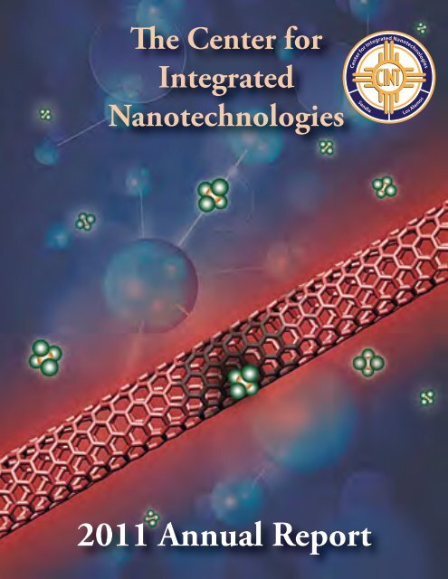
2011 Annual Report - Center for Integrated Nanotechnologies - Los ...
2011 Annual Report - Center for Integrated Nanotechnologies - Los ...
2011 Annual Report - Center for Integrated Nanotechnologies - Los ...

You also want an ePaper? Increase the reach of your titles
YUMPU automatically turns print PDFs into web optimized ePapers that Google loves.
The <strong>Center</strong> <strong>for</strong><br />
<strong>Integrated</strong><br />
<strong>Center</strong> <strong>for</strong> <strong>Integrated</strong> <strong>Nanotechnologies</strong><br />
<strong>Nanotechnologies</strong><br />
Sandia<br />
<strong>Los</strong> Alamos<br />
<strong>2011</strong> <strong>Annual</strong> <strong>Report</strong><br />
1
<strong>Center</strong> <strong>for</strong> <strong>Integrated</strong> <strong>Nanotechnologies</strong><br />
<strong>2011</strong> <strong>Annual</strong> <strong>Report</strong><br />
Editor and Designer - Antonya Sanders<br />
Content and Office Support - Heather Brown, Linda Chavez, Corey Parsons<br />
Contributing writers - Caroline Spaeth, Fransisco Ojeda, Neal Singer, Linda Peteanu<br />
Photographer - Robert Kramer<br />
LA-UR--12-22414<br />
Cover art - Artist’s concept of nanotubes on the liquid surface. Image from <strong>Los</strong> Alamos National Laboratory<br />
2<br />
2The <strong>Center</strong> <strong>for</strong> <strong>Integrated</strong> <strong>Nanotechnologies</strong> | <strong>2011</strong> <strong>Annual</strong> <strong>Report</strong>
Table of Contents<br />
Table of Contents<br />
4 From the Directors’ Office<br />
6 News from <strong>2011</strong><br />
10 Integration Focus Activities<br />
Nanowires <strong>for</strong> New Energy Concepts IFA<br />
Programmable Membrane-Based Nanocomposites IFA<br />
Metamaterials and Plasmonics IFA<br />
13 Discovery Plat<strong>for</strong>ms<br />
Nanowire Discovery Plat<strong>for</strong>m (NWDP)<br />
Nanomechanics and Thermal Transport Discovery Plat<strong>for</strong>m (NMTTDP)<br />
TEM Liquid Cell Discovery Plat<strong>for</strong>m<br />
Microfluidic Synthesis Discovery Plat<strong>for</strong>m<br />
16 <strong>2011</strong> CINT-funded Postdocs<br />
Postdoc Highlight - Julio Martinez<br />
18 CINT User Program<br />
Users Executive Committee<br />
3D Tracking of Proteins - Jim Werner and Diane Lidke<br />
CINT User Conference <strong>2011</strong><br />
22 Nanophotonics and Optical Nanomaterials Thrust<br />
Nonresonant Broadband Funneling of Light via Ultrasubwavelength Channels<br />
CINT scientists detect and track single molecules with nanoscale carbon cylinders<br />
Scientist highlight: Jen Hollingsworth<br />
<strong>Los</strong> Alamos researchers unravel the mystery of quantum dot blinking<br />
28 Nanoscale Electronics and Mechanics Thrust<br />
Enhanced superconducting properties through integration of NbC with highly aligned<br />
CNT <strong>for</strong>est<br />
Controlling the interface width in Si/Ge nanowire heterojunctions<br />
Voltage increases up to 25% observed in closely packed nanowires<br />
32 Soft, Biological and Composite Nanomaterials Thrust<br />
Nanocomposite encapsulation of biological samples <strong>for</strong> long-term storage and transport<br />
Wally Paxton - CINT Scientist highlight<br />
Directing cellular morphogenesis and polarization using nanoscale chemical and topological<br />
cues<br />
37 Theory and Simulation of Nanoscale Phenomena Thrust<br />
Electronic Fingerprints of DNA Bases on Graphene<br />
Potential New Nanolithography Tool from Directed Assembly of Mixed Polymer Brushes<br />
Induced polarization at a paraelectric/superconducting interface<br />
42 Contact In<strong>for</strong>mation<br />
43 Awards<br />
3
From the Directors’ Office<br />
We are pleased to share with you this <strong>2011</strong> edition of<br />
the <strong>Annual</strong> <strong>Report</strong> from the <strong>Center</strong> <strong>for</strong> <strong>Integrated</strong> <strong>Nanotechnologies</strong><br />
(CINT) and the growing excitement we feel<br />
around cementing our brand as a leader in integration<br />
nanoscience. This can be seen most readily in the momentum<br />
we have achieved in our signature Integration<br />
Focus Activities (IFAs). These ef<strong>for</strong>ts unite our scientists<br />
across our four scientific Thrust areas with our users to<br />
concentrate research on larger-scale nanoscience integration<br />
challenges <strong>for</strong> specific classes of nanomaterials,<br />
systems, and phenomena. All three of our current IFAs (p.<br />
10) now have a full head of steam, and nearly 30% of our<br />
current user projects map in some meaningful way to one<br />
of these IFAs. As part of our redoubled ef<strong>for</strong>t to increase<br />
our industrial user base, we are also looking to leverage<br />
these IFAs to build a stronger link to and spur recruitment<br />
within our industrial user community. We believe that the<br />
IFAs are a natural community-building tool with an intrinsic<br />
value proposition <strong>for</strong> industry; an R&D pipeline that can<br />
lead to more mature, more commercially well-positioned<br />
technologies. Finally, as nanoscience and nanotechnology<br />
are maturing, we as a research community are beginning<br />
to see our ef<strong>for</strong>ts extend in many exciting new directions.<br />
Our focus on nanoscience integration positions us<br />
very well to capitalize on new opportunities including the<br />
emerging Mesoscale Initiative within the DOE Office of<br />
Science. Many aspects of mesoscale science are embodied<br />
in the integration of nanoscale building blocks.<br />
We are equally proud of our continuing strong per<strong>for</strong>mance<br />
in support of our user program. We have fully<br />
transitioned to our new user proposal database providing<br />
enhanced convenience and flexibility <strong>for</strong> proposal submission<br />
and review. In our two regular proposal calls this year<br />
we received a total of 225 proposals, an increase of 10%<br />
over our 2010 per<strong>for</strong>mance. Our official count on number<br />
of users <strong>for</strong> the period remains at ~ 350 and continues<br />
to reflect full engagement of our scientific staff. We are<br />
also seeing a steady increase in our industrial user base,<br />
with the number of industrial proposals (including Rapid<br />
Access proposals) doubling in <strong>2011</strong>. We attribute this in<br />
part of our outreach ef<strong>for</strong>ts including our focused industrial<br />
session in each of our past two annual User Conferences<br />
(p. 20)<br />
As always, we welcome feedback and invite suggestions<br />
from our users and all stakeholders on all aspects of our<br />
user program and <strong>Center</strong> operations. We hope you find<br />
this annual report in<strong>for</strong>mative and, more importantly, that it<br />
will motivate you to continue your engagement with CINT<br />
or to become a CINT user.<br />
David Morris, Director Neal Shinn, Co-Director S. Tom Picraux, Chief Scientist<br />
Heather Brown,<br />
User Program Coordinator<br />
Antonya Sanders,<br />
Communications Coordinator<br />
4<br />
4The <strong>Center</strong> <strong>for</strong> <strong>Integrated</strong> <strong>Nanotechnologies</strong> | <strong>2011</strong> <strong>Annual</strong> <strong>Report</strong>
About CINT<br />
The <strong>Center</strong> <strong>for</strong> <strong>Integrated</strong> <strong>Nanotechnologies</strong> (CINT) is a Department<br />
of Energy/Office of Science Nanoscale Science Research<br />
<strong>Center</strong> (NSRC) operating as a national user facility devoted<br />
to establishing the scientific principles that govern the design,<br />
per<strong>for</strong>mance, and integration of nanoscale materials. Jointly<br />
operated by <strong>Los</strong> Alamos and Sandia National Laboratories, CINT<br />
explores the continuum from scientific discovery to use-inspired<br />
research, with a focus on the integration of nanoscale materials<br />
and structures to achieve new properties and per<strong>for</strong>mance and<br />
their incorporation into the micro- and macro worlds. Through its<br />
Core Facility at Sandia National Laboratories and its Gateway<br />
Facility at <strong>Los</strong> Alamos National Laboratory, CINT provides open<br />
access to tools and expertise needed to explore the continuum<br />
from scientific discovery to the integration of nanostructures<br />
into the micro- and macro worlds. In its overall operations, CINT<br />
strives to achieve the following goals common to all Nanoscale<br />
Science Research <strong>Center</strong>s:<br />
1. Conduct <strong>for</strong>efront research in nanoscale science;<br />
2. Operate as a user facility <strong>for</strong> scientific research;<br />
3. Provide user access to the relevant BES-supported<br />
expertise and capabilities at the host national laboratory;<br />
4. Leverage other relevant national laboratory capabilities<br />
to enhance scientific opportunities <strong>for</strong> the nanoscience<br />
user community;<br />
These additional goals are specific to the unique CINT mission:<br />
5. Establish and lead a scientific community dedicated to solving<br />
nanoscale science integration challenges;<br />
6. Create a single user facility program that combines expertise<br />
and facilities at both <strong>Los</strong> Alamos and Sandia National<br />
Laboratories.<br />
The CINT user program provides the international scientific community<br />
with open access to world-class scientific staff and stateof-the-art<br />
facilities <strong>for</strong> theory and simulation, nanomaterials synthesis<br />
and characterization, and unique capabilities <strong>for</strong> nanoscale<br />
materials integration, from the level of nanoscale synthesis to the<br />
fabrication of micro- and macroscale structures and devices. The<br />
staff of CINT includes laboratory scientists, postdocs and technical<br />
support staff who are leaders in the nanoscience research<br />
programs in CINT scientific thrust areas:<br />
• Nanoscale Electronics and Mechanics,<br />
• Nanophotonics and Optical Nanomaterials,<br />
• Soft, Biological and Composite Nanomaterials, and<br />
• Theory and Simulation of Nanoscale Phenomena.<br />
The thrusts have been developed over the past several years by<br />
engaging the broader scientific community through discussions<br />
with potential CINT users and with attendees at CINT workshops,<br />
as well as by attracting some of today’s top nanoscience talent to<br />
become CINT staff.<br />
5
News from <strong>2011</strong><br />
News from <strong>2011</strong><br />
CINT Technologist Chris Sheehan putting a sample into the Magellan SEM<br />
: New Capabilities<br />
Featured capability:<br />
CINT Magellan HRSEM (High Resolution Electron Microscope)<br />
The FEI Magellan 400 SEM provides sub-nanometer spatial resolution from 1kV to 30 kV.<br />
By using low voltages, only the surface of the sample interacts with the electron beam<br />
and thus insulators/beam sensitive samples can be imaged without the need <strong>for</strong> conductive<br />
coatings and the amount of surface data is maximized. These capabilities make this<br />
tool ideal <strong>for</strong> investigations of nanotubes, nanowires, nanocomposites, and other materials<br />
where workhorse SEMs do not have the low-voltage resolution required <strong>for</strong> sensitive surface<br />
imaging. This system features:<br />
• Schottky thermal emission source with UniColore<br />
mode to give a highly coherent beam (less<br />
than 0.2 eV energy spread)<br />
• spatial resolutions of 0.8 nm at 1kV and above<br />
in secondary electron mode.<br />
• EDAX Apollo XV Energy Dispersive Spectroscopy<br />
(EDS) detector <strong>for</strong> elemental analysis.<br />
• EDAX Hikari Electron Backscatter Diffraction<br />
(EBSD) detector <strong>for</strong> crystallographic orientation<br />
determination.<br />
• Nabity electron beam lithography patterning<br />
capability.<br />
• annular STEM detector (spatial resolution of 0.7<br />
nm).<br />
Scientific contacts: Chris Sheehan and Nathan Mara<br />
InP/ZnSe quantum dots taken in STEM mode,<br />
looking through very thin carbon film with the<br />
QDs sitting on it. These measured to be 5 nm,<br />
+/- 1nm.<br />
Other new capabilities:<br />
Holographic Optical Trapping Microscope<br />
The holographic trapping microscope enables the non-contact<br />
optical manipulation of soft materials and nanoparticles and can<br />
also mechanically and spectroscopically probe such materials<br />
in situ. Force measurements based on optical manipulation<br />
methods can be used to investigate the viscoelastic properties of<br />
soft and biological materials or probe adhesion <strong>for</strong>ces. Contact:<br />
Walter Paxton<br />
Nanoink Dip-Pen Nanolithography<br />
Dip-Pen Nanolithography is a scanning probe lithography technique<br />
where a “tip” (e.g., an AFM tip or tip-array) is used to “write”<br />
liquid-phase “inks” onto any substrate with 50 nm to 10 μm resolution.<br />
The inks can comprise solutions of self-assembled-monolayer-(SAM)<br />
<strong>for</strong>ming molecules, pure liquids, nanoparticles, biomolecules,<br />
sol-gel precursors, etc. DPN operates under ambient<br />
conditions and is fully compatible with biomolecules, polymers,<br />
and quantum nanostructures. Contact: Jennifer Hollingsworth<br />
IChrome TVIS Super Continuum Source<br />
This versatile light source serves as an excitation source <strong>for</strong><br />
measuring photoluminescence lifetimes down to 1 ps, enables<br />
photon correlation measurements (when paired with the recently<br />
procured time-correlated single-photon counting instrumentation),<br />
provides a bright tunable source <strong>for</strong> single-nanoelement PL imaging/spectroscopy<br />
and <strong>for</strong> pump-probe measurements, and serves<br />
as the basis <strong>for</strong> new imaging modes and spectroscopy including<br />
Rayleigh scattering imaging and absorbance spectroscopy at<br />
single-element levels. Contact: Steve Doorn<br />
Hysitron PI-85 SEM Picoindenter<br />
This in-situ SEM strain stage represents a significant capability<br />
enhancement in support of CINT’s signature ef<strong>for</strong>ts in in-situ<br />
nanomechanics. The system has a load range from 1µN to<br />
30mN, offers in-situ indentation, bending, compression and tension<br />
testing capabilities, includes a heating stage rated to 400°C,<br />
an electrical characterization package and has outstanding resolution<br />
of both load (
R&D 100 Award: NanoCluster Beacons<br />
News from <strong>2011</strong><br />
CINT scientists won one of R&D Magazine’s <strong>2011</strong> R&D 100 Awards <strong>for</strong> their work with NanoCluster Beacons. Recognized as the<br />
“Oscars of Invention” by the Chicago Tribune, these awards honor the top 100 proven technological advances of the past year.<br />
NanoCluster Beacons are collections of silver atoms<br />
maneuvered to illuminate when bound to specific nucleic<br />
acids, such as the DNA of particular pathogens. Created by<br />
Hsin-Chih (Tim) Yeh, James Werner, Jaswinder Sharma,<br />
and Jennifer Martinez, these beacons can be used to probe<br />
<strong>for</strong> diseases that threaten humans by identifying the nucleic<br />
acid targets that represent a person’s full genome, and allow<br />
<strong>for</strong> personalized medication. They also can be used in<br />
quantitative biology applications, such as counting individual<br />
molecules inside a cell.<br />
Once bound with a specific target, a NanoCluster Beacon<br />
lights up, emitting fluorescence approximately 200 times<br />
greater than in the unbound state and easily viewed by the<br />
naked eye under ultraviolet light. The beacons come in an<br />
array of colors <strong>for</strong> multiplexed analyses, are more photostable<br />
than beacons used today, and can be turned on and<br />
off reversibly. Inexpensive, easy to use, and reversible,<br />
NanoCluster Beacons are superior molecular probes <strong>for</strong><br />
detecting specific targets, human oncogene (cancer) sequences,<br />
and molecular disease sequences (such as sickle<br />
cell anemia).<br />
Patents<br />
CINT Postdoc Hsin-Chih (Tim) Yeh was part of the NanoCluster Beacons team.<br />
CINT Scientists were involved in the following patent<br />
applications in <strong>2011</strong>-2012 (does not include disclosures).<br />
• Thick-shell nanocrystal quantum dots. Jennifer<br />
Hollingsworth et al., US Patent US 7,935,419 B1<br />
Issued May 3, <strong>2011</strong>.<br />
• Polymer-assisted deposition of films. T. M.<br />
McCleskey, A. K. Burrell, Q. X. Jia, and Y. Lin,<br />
US Patent No. 8,124,176, Issued Feb. 28, 2012.<br />
• Fibrous composites comprising carbon nanotubes<br />
and silica. H. Peng, Y. T. Zhu, D. E. Peterson,<br />
and Q. X. Jia, US Patent No. 8,034,448,<br />
Issued Oct. 11, <strong>2011</strong>.<br />
• Buffer layers <strong>for</strong> coated conductors. L. Stan,<br />
Q. X. Jia, and S. R. Foltyn, US Patent No.<br />
8,003,571, Issued Aug. 23, <strong>2011</strong>.<br />
• Carbon microtubes. H. Peng, Y. T. Zhu, D. E. Peterson,<br />
and Q. X. Jia, US Patent No. 7,959,889,<br />
Issued June 14, <strong>2011</strong>.<br />
• Preparation Of Anode Comprising Silicon<br />
Nanowires. J.-H. Cho and S. T. Picraux Provisional<br />
application (S121,996). Filed.<br />
• Carbon nanotube/metal carbide composites with<br />
enhanced properties. G. Zou, Y. Zhang, A. K. Burrell, T. M. McCleskey, and Q. X. Jia, Filed.<br />
• Room temperature ferromagnetism insulating thin films. J. MacManus-Driscoll and Q. X. Jia, Filed.<br />
• Mid-Infrared Tunable Metamaterials , I. Brener et al., Filed<br />
• Magnetic Agglomeration Method <strong>for</strong> Size Control in the Synthesis of Magnetic Nanoparticles, D. Huber, US Patent No.<br />
7972410, Issued July 5, <strong>2011</strong>.<br />
• High-Yield synthesis of bookite TiO2 nanoparticles, D. Huber and T.C. Monson, US Patent No. 7943116, Issued May 17, <strong>2011</strong><br />
7
News from <strong>2011</strong><br />
Journal & Book Covers<br />
Optical imaging approaches are used to characterize<br />
the interactions of CdSe quantum dots (QDs) with<br />
live immune cells in order to gain insight into particle<br />
shape and size-dependent behavior. Through the use<br />
of total internal reflectance fluorescence (TIRF) and<br />
hyper-spectral confocal microscopy (HCM), Timlin and<br />
co-workers are able to characterize particle diffusion<br />
and partitioning within the plasma membrane, cellular<br />
uptake kinetics, as well as sorting of particles into<br />
lysomes. TIRF imaging reveals that rod-shaped QDs are<br />
internalized into the cell two-to-three times more slowly<br />
than more spherical ones, and HCM suggests that QDs<br />
tend to partition within the cell membrane into regions<br />
containing a single particle type.<br />
CINT Contact: George Bachand<br />
Articles published week of 11 JULY <strong>2011</strong><br />
Volume 99 Number 2<br />
APPLIED<br />
PHYSICS<br />
LETTERS<br />
Synthesis of germanium/silicon (Ge/Si) core/shell<br />
nanowire heterostructures is typically accompanied<br />
by unwanted gold (Au) diffusion on the Ge nanowire<br />
sidewalls, resulting in rough surface morphology,<br />
undesired whisker growth, and detrimental<br />
per<strong>for</strong>mance of electronic devices. Here, we advance<br />
understanding of this Au diffusion on nanowires, its<br />
diameter dependence and its kinetic origin. We devise<br />
a growth procedure to <strong>for</strong>m a blocking layer between<br />
the Au seed and Ge nanowire sidewalls leading to<br />
elimination the Au diffusion <strong>for</strong> in situ synthesis of high<br />
quality Ge/Si core/shell heterostructures.<br />
CINT Contact: Tom Picraux<br />
Downloaded on 30 May 2012<br />
Published on 22 March <strong>2011</strong> on http://pubs.rsc.org | doi:10.1039/C1SM90019F<br />
Showcasing research from Dr Haiqing Liu and<br />
Dr George Bachand at Sandia National<br />
Laboratories, Albuquerque, USA<br />
Title: Understanding energy dissipation and thermodynamics in<br />
biomotor-driven nanocomposite assemblies<br />
A nanocomposite ring <strong>for</strong>med by the motor protein-drive,<br />
dynamic self-assembly of microtubule filaments and nanocrystals<br />
quantum dots. Manipulation of the energy dissipative and<br />
thermodynamic components of this system enables the assembly<br />
of nanocomposites with varying structural morphologies.<br />
As featured in:<br />
See Bachand et al.,<br />
Soft Matter, <strong>2011</strong>, 7, 3087.<br />
www.rsc.org/softmatter<br />
Registered Charity Number 207890<br />
A nanocomposite ring <strong>for</strong>med by the motor<br />
protein-drive, dynamic self-assemblyof microtubual<br />
filaments and nanocrystals quantum dots.<br />
Manipulation of the energy dissipative and<br />
thermodynamic components of this system enables<br />
the assembly of nanocomposites with carying<br />
structural morphologies.<br />
CINT Contact: George Bachand<br />
Volume 7 | Number 7 | <strong>2011</strong> Soft Matter Includes a collection of articles on the theme of Active Soft Matter Pages 3025–3652<br />
ww<br />
ISSN<br />
CINT Scientist, Rohit Prasankumar, and CINT<br />
Distinguished Affiliate, Toni Taylor edited a book<br />
in <strong>2011</strong>, titled “Optical Techniques <strong>for</strong> Solid-State<br />
Materials Characterization.”<br />
A nanowire image from Tom Picraux’s team was<br />
edited and used <strong>for</strong> the book cover of “Silicon and<br />
Silicide Nanowires: Applications Fabrication and<br />
Properties.”<br />
8<br />
8The <strong>Center</strong> <strong>for</strong> <strong>Integrated</strong> <strong>Nanotechnologies</strong> | <strong>2011</strong> <strong>Annual</strong> <strong>Report</strong>
News from <strong>2011</strong><br />
NSRC Events<br />
NSRC Contractors meeting<br />
From May 31-June 2, <strong>2011</strong>, representatives from the Department of Energy Basic Energy Science Nanoscale Science Reserach<br />
<strong>Center</strong>s (NSRCs) and E-Beam Micro-characterization <strong>Center</strong>s gathered in Maryland <strong>for</strong> the <strong>2011</strong> Contractors’ Meeting. The purpose<br />
of the Contractors’ Meeting is to bring together researchers - facility scientists and facility users of the BES EBMC and NSRC facilities<br />
and leading experts across the multi-disciplinary spectrum<br />
served by these facilities - to foster discussion 19<br />
of the latest research results, catalyze collaborations,<br />
and stimulate ideas <strong>for</strong> promising new directions <strong>for</strong> Our Novel SiNW Synthesis Method<br />
investigation. Dynamic exploration of research ideas<br />
and capability needs will also help DOE in assessing<br />
the needs of the research community to chart future<br />
program directions.<br />
CINT was featured in the meeting with presentations<br />
by CINT Scientist Jianyu Huang titled In-Situ TEM<br />
Electrochemistryof Li-Ion Battery Materials, and CINT<br />
User Dan Gianola from University of Pennsylvania<br />
with a talk on Quantative In-Situ Mechanical Testing<br />
of Nanowires. There were also 12 poster presentations<br />
from a combination of CINT Users, scientist, and<br />
postdocs.<br />
Wafer-scale control of shape,<br />
length, spacing, doping, and<br />
axial and face orientation<br />
MRS Meeting<br />
The NSRCs continue to work to<br />
attract new users. One method<br />
is to host a booth at some of<br />
the larger technical conferences<br />
that attract potential<br />
users. In <strong>2011</strong>, the NSRCs<br />
joined together at the Materials<br />
Research Society Fall Meeting<br />
in Boston.<br />
Left to right - Grace Webster<br />
from the <strong>Center</strong> <strong>for</strong> Functional<br />
Nanomaterials (CFN), Laura<br />
Edwards representing the<br />
<strong>Center</strong> <strong>for</strong> Nanophase Materials<br />
Sciences (CNMS), Antonya<br />
Sanders from CINT, and Denean<br />
McArthur also of CFN.<br />
9
Integration Focus Activities<br />
Integration Focus Activities<br />
Integration Focus Activities (IFAs) are initiatives aimed at nanoscale integration challenges within the context of specific classes<br />
of materials, systems, or phenomena that will have high scientific and technological impact. These topics are developed from a<br />
“bottoms-up” process within the CINT community. They are cross-thrust activities, which provide canonical examples of integration<br />
science and are intended to become strong attractors <strong>for</strong> users and collaborators. The IFAs both emerge out of a particular thrust ef<strong>for</strong>t<br />
and build on areas of strength across thrusts. The studies center on particular classes of materials, systems, or phenomena and<br />
derive their integration focus through a use-inspired science approach. These focused ef<strong>for</strong>ts bring an interdisciplinary approach by<br />
CINT scientists and users to a particularly timely area of integration science. They enable rapid progress in specific areas of common<br />
interest, attract and build user communities, and are variable term in nature. Each IFA is supported by two dedicated postdoc positions<br />
whose research is targeted towards linking the work of CINT scientists and the user community in specific high-impact areas.<br />
Nanowires <strong>for</strong> New Energy Concepts IFA<br />
The novel properties of nanowires offer tremendous opportunities<br />
<strong>for</strong> trans<strong>for</strong>mative energy applications. These multi-purpose<br />
materials combine nanoscale and even quantum-confinement<br />
effects with enhanced transport properties. CINT scientists<br />
together with our user community are focusing to understand and<br />
control the functionality and integration of heterogeneous semiconducting<br />
nanowires <strong>for</strong> new energy harvesting and storage<br />
concepts. We emphasize heterogeneous nanowires to realize<br />
an unprecedented level of control over material per<strong>for</strong>mance by<br />
tuning interface, strain, and materials-mixing effects. We combine<br />
new synthesis strategies with structural, electrical, optical,<br />
and thermal characterization, initially at the single-nanowire level<br />
to answer critical science questions underlying new nanowire<br />
materials concepts <strong>for</strong> photovoltaics, thermoelectrics, and energy<br />
storage. We also drive toward functional integration of nanowires<br />
into two- and three-dimensional architectures.<br />
- Ultrafast optical spectroscopy. The ultrafast optical microscopy<br />
(UOM) system uses a femtosecond pump-probe laser setup and<br />
microscope objectives to measure carrier dynamics and carrier<br />
velocities in single nanowires with high temporal and spatial<br />
resolution in a non-contact, non-invasive manner. We showed<br />
the first measurement of carrier-lifetime increase by surface passivation<br />
on a single Si-SiO2 nanowire. By spatially separating the<br />
pump and the probe along the nanowire we extracted the carrier<br />
transport along the nanowire axis. We also used this system to<br />
per<strong>for</strong>m the first measurement of GaN/AlGaN core/shell nanowires<br />
that revealed the influence of the AlGaN shell on carrier<br />
relaxation.<br />
Selected Recent Highlights:<br />
- Flow-reactor solution-liquid-solid nanowire synthesis. We’ve<br />
developed a flow reactor <strong>for</strong> solution phase growth of heterostructured<br />
nanowires. In contrast to traditional “beaker” chemistry<br />
the volume of reactants in the flow cell is very small. This<br />
enables rapid and precisely controlled switching of the reactants<br />
that makes growing axially heterostructured nanowires possible.<br />
Using this technique we have shown the first example of<br />
an eight-segment ZnSe-CdSe axially heterostructured nanowire.<br />
By controlling the growth rate in the flow reactor we measured<br />
the length-diameter dependence of CdSe and ZnSe nanowires<br />
and determined <strong>for</strong> the first time that the solution-phase growth<br />
mechanism involves both the Gibbs-Thomson effect and surface<br />
diffusion.<br />
- Toward Si colar cells with single crystal efficiency at thin film<br />
cost. Using radial p-i-n nanowire arrays, we aim to decouple optical<br />
absorption and carrier collection. We have gained new insight<br />
into nanoscale radial epitaxial, low-temperature single crystal<br />
growth and fabrication of large-area nanowire arrays. We have<br />
measured external and internal quantum efficiencies by conducting<br />
wavelength dependent photovoltaic and optical absorption<br />
measurements in collaboration with our industrial partners.<br />
10<br />
10The <strong>Center</strong> <strong>for</strong> <strong>Integrated</strong> <strong>Nanotechnologies</strong> | <strong>2011</strong> <strong>Annual</strong> <strong>Report</strong>
Integration Focus Activities<br />
Programmable Membrane-Based Nanocomposites IFA<br />
The focus of the Programmable<br />
Membrane-Based Nanocomposites<br />
(PMBN) Focus Area is<br />
to investigate the interactions<br />
between nanoscale materials<br />
and membrane-based composites<br />
such as lipid and polymer<br />
vesicles and membrane architectures.<br />
The ultimate goals of<br />
the research involve learning<br />
how to replicate many of the<br />
complex behaviors associated<br />
with cellular membranes within<br />
artificial nanocomposites and<br />
integrated systems. These integrated<br />
nanomaterials could be<br />
utilized in applications including<br />
electrical energy storage (the<br />
artificial electric eel), artificial<br />
photosynthesis, environmental<br />
remediation (reversible<br />
CO2 sequestration and water<br />
purification), and responsive<br />
sensors and adaptive materials<br />
<strong>for</strong> Homeland Defense applications.<br />
The starting point <strong>for</strong> understanding<br />
the behavior of<br />
complex membranes involves<br />
understanding the fundamental<br />
interactions between membrane<br />
hosts, nanoparticles,<br />
and substrate surfaces. Initially,<br />
research in this IFA focused<br />
on investigating interactions of nanoparticles with lipid-based<br />
membrane systems, including: 1) nanoparticle adsorption, insertion,<br />
migration, and aggregation as a function of particle size,<br />
shape, and surface chemistry, 2) lipid responses as mediated by<br />
substrate interactions, including diffusion and transport, mechanical<br />
stability, domain <strong>for</strong>mation and component partitioning, and 3)<br />
membrane-mediated nanoparticle organization.<br />
Over the last year, research has shifted focus to polymer-based<br />
membrane materials. Polymers have the advantage of added<br />
versatility providing a greater means of tuning functionality, molecular<br />
weight, and robustness, while allowing <strong>for</strong> self-assembly<br />
into similar membrane organization with similar properties observed<br />
in lipid-based systems. We recently showed the ability of<br />
<strong>for</strong>ming hybrid polymer bilayer/monolayer structures by surface<br />
chemistry in a one-step procedure using polymer micelles as the<br />
starting material. The hybrid layers resulted in self-assembled<br />
independent compartmentalization with differing properties.<br />
These hybrid systems are being further investigated as hosts <strong>for</strong><br />
nanoparticles and as biomimetic films.<br />
Over the next year we will continue developing polymer-based<br />
membrane materials from self-assembly of block copolymers.<br />
Systems being developed are more elaborate with an emphasis<br />
placed on functional properties to enhance nanomaterials<br />
interaction and control. As an example, responsive polymers<br />
and functional polymers (e.g. conjugated) are being explored as<br />
potential polymer blocks. We are also beginning work on a new<br />
project area that incorporates theoretical simulations, chemical<br />
synthesis, and experimental verification to define parameters <strong>for</strong><br />
controlling the interaction and organization of nanoparticles with<br />
polymer brushes. Using mixed polymer brushes, consisting of<br />
locally phase separated regions of two polymers, functionalized<br />
nanoparticles will be localized spatially. For polymers that are<br />
responsive to the either the pH of the solvent or temperature,<br />
the nanoparticles can be captured and released in a controlled<br />
manner. For this work, we are using grafted polymer brushes in<br />
order to control the amount of each polymer in mixed systems.<br />
Uni<strong>for</strong>m sized and shaped nanoparticles, essential to nanoelectronic<br />
engineering with defined predicted properties, will be<br />
synthesized. The polymer layer will be designed with specific<br />
interactions to drive self-assembly. Molecular simulations will<br />
correlate the interactions on the nanometer length scale with<br />
the macroscopic assemblies in solutions and at interfaces. Both<br />
explicit atom and coarse grained models will be used to cover<br />
the large range of time and length scale inherent in polymeric<br />
systems. Both experiment and simulation will follow the infiltration<br />
of nanoparticles from solution into the polymer brush in solution<br />
and the subsequent structure of the nanoparticle/brush film after<br />
the solvent is removed. The properties of the composite film,<br />
both mechanical and responsiveness will be studied <strong>for</strong> potential<br />
applications.<br />
11
Integration Focus Activities<br />
Metamaterials and Plasmonics IFA<br />
Artificially structured metamaterials and plasmonics provide novel<br />
properties that are difficult or impossible to achieve using naturally<br />
occurring materials. The new class of electromagnetic artificial<br />
materials greatly extends our ability to manipulate electromagnetic<br />
radiation (light), and has led to the demonstration of unique<br />
behavior such as negative refraction, cloaking, and superlensing.<br />
The Metamaterials and Plasmonics Integration Focus Activity<br />
builds upon the extensive activities at CINT in this field over the<br />
past few years spanning from terahertz to optical wavelengths.<br />
The goals of these activities are to understand and design metamaterial<br />
and plasmonic structures capable of enhanced interactions<br />
with light, and to accomplish novel functionalities from<br />
tunable and nonlinear hybrid metamaterials through integration of<br />
semiconducting and/or complex oxide materials and structures.<br />
During the past years CINT has demonstrated leadership in this<br />
field through the groundbreaking work in novel metamaterial<br />
structures, active and dynamical metamaterials and plasmonics,<br />
and their applications to sensing and imaging.<br />
During the last year the research in this IFA has largely focused<br />
on the enhanced light-matter interactions when metamaterial or<br />
plasmonc structures are introduced. We found that the phonon<br />
vibrations in the integrated (substrate) materials or the intersubband<br />
transitions in semiconducting quantum wells can be<br />
strongly coupled to the metamaterial resonances, which might result<br />
in loss reduction in metamaterials and the creation of unique<br />
spectral features. Enhanced nonlinear response was predicted in<br />
the early days of metamaterial research, and recently it has become<br />
an important research direction. We found that, in addition<br />
to their wide range thermal and optical tunability of the resonant<br />
response, high-temperature superconducting metamaterials<br />
exhibit strong nonlinear response under intense terahertz irradiation.<br />
Recent highlights also include the prediction of nonresonant<br />
broadband light transmission in a nano plasmonic structure, the<br />
demonstration of broadband metamaterial perfect absorbers and<br />
identification of the mechanism, and the demonstration of alldielectric<br />
low loss metamaterials in the infrared.<br />
Through a vibrant network of users and research groups at both<br />
National Labs, this IFA will continue its work and leadership in<br />
these areas of Metamaterials and Plasmonic research. Additional<br />
expansion into new directions include integrated active metamaterial<br />
devices as diffraction modulator <strong>for</strong> terahertz imaging,<br />
active or dynamical tuning of chirality in 3-D metamaterials and<br />
electromagnetically induced transparency in superconducting<br />
metamaterials, light polarization control and conversion, using<br />
spoof plasmon <strong>for</strong> thermal emission control and enhanced emission,<br />
integration of metamaterial and plasmonic resonators with<br />
epitaxial bandgap engineered heterostructures and complex oxides<br />
<strong>for</strong> enhanced nonlinear responses, including superconducting<br />
Josephson junctions towards quantum metamaterials, and<br />
the coupling of plasmonic structures with optical nanoparticles<br />
such as quantum dots, nanowires, carbon nanotubes and other<br />
semiconductor heterostructures.<br />
12<br />
12The <strong>Center</strong> <strong>for</strong> <strong>Integrated</strong> <strong>Nanotechnologies</strong> | <strong>2011</strong> <strong>Annual</strong> <strong>Report</strong>
Discovery Plat<strong>for</strong>ms<br />
Discovery Plat<strong>for</strong>ms <br />
The thrusts develop a variety of new instrumentation to advance<br />
the science in their areas. One ef<strong>for</strong>t unique to CINT is the Discovery<br />
Plat<strong>for</strong>m. These plat<strong>for</strong>ms are modular micro-laboratories<br />
designed and batch fabricated by CINT to allow easy integration<br />
of nanomaterials into microscale structures. Their purpose is<br />
to facilitate studies of nanomaterial properties and their integration.<br />
They should allow easy connections, a range of diagnostic<br />
and experimental measurement conditions, and a degree of<br />
standardization and reproducibility in nanoscale measurements.<br />
The inception, creation and evolution of Discovery Plat<strong>for</strong>ms have<br />
evolved in close collaboration with our user community.<br />
Nanowire Discovery Plat<strong>for</strong>m (NWDP)<br />
One configuration of the CINT Nanowire Discovery Plat<strong>for</strong>m<br />
(NWDP), the lateral nanowire (NW) plat<strong>for</strong>m, has completed<br />
fabrication at Sandia’s microelectronics fabrication facility and has<br />
been under initial testing. This plat<strong>for</strong>m contains a high density<br />
array of metallic interconnects with buried bottom gates <strong>for</strong> the assembly<br />
and electrical characterization of semiconducting nanowires.<br />
The electrodes were designed to enable the assembly of<br />
nanowires from solution using dielectrophoresis (DEP). Scoping<br />
experiments using silicon nanowires showed successful DEP assembly<br />
with future work being focused on electrical characterization<br />
of the assembled nanowires. A second version of the NWDP,<br />
the silicon nanowire DP, has almost emerged from full fabrication.<br />
This DP is distinguished by the monolithic integration of silicon<br />
nanowires as an intrinsic part of the plat<strong>for</strong>m, i.e. the NWs are<br />
fabricated as part of the NWDP fabrication process. The integrated<br />
NWs are designed to enable concepts of NW-based device<br />
and sensor characterization without need <strong>for</strong> post-fabrication NW<br />
integration. The third version of the NWDP, the vertical NW DP,<br />
has completed partial processing, but issues with the thick isolation<br />
dielectric were found. This plat<strong>for</strong>m is being held from further<br />
processing until a solution to the dielectric failure issue can be<br />
found.<br />
1.5 mm<br />
<br />
<br />
<br />
3.5 mm<br />
Our future work on the NWDP will be focused on evaluation of<br />
the completed lateral NW plat<strong>for</strong>m. We will use dielectrophoresis<br />
to assemble semiconducting nanowires across electrodes and<br />
over the top of buried electrical interconnects. The evaluation will<br />
use silicon and silicon-germanium nanowires synthesized in the<br />
CINT VLS NW growth facility, with a special interest in investigating<br />
axially-doped wires (i.e. having axial pn junctions). Following<br />
assembly, the buried gates will be used to modulate the NW<br />
conductance <strong>for</strong> evaluation of the per<strong>for</strong>mance of these NWs in<br />
nanoelectronics and NW-based sensing.<br />
13
Discovery Plat<strong>for</strong>ms<br />
Nanomechanics and Thermal Transport Discovery Plat<strong>for</strong>m (NMTTDP)<br />
CINT’s ‘Nanomechanics and Thermal Transport Discovery<br />
Plat<strong>for</strong>m’ (NMTTDP) has been heavily used by researchers <strong>for</strong><br />
the study of the nanomechanics of semiconducting and metallic<br />
nanowires. In work per<strong>for</strong>med by CINT user Prof. Dan Gianola<br />
and his research group at U. Penn, the NMTTDP was used to<br />
measure the piezoresistance of (100)-oriented silicon nanowires<br />
as a function of wire diameter and length. These studies required<br />
electrical testing during straining, which is one key feature<br />
that was added in the second generation of this nanomechanics<br />
test plat<strong>for</strong>m. Their studies revealed gauge factors comparable<br />
to values reported <strong>for</strong> thin film silicon and in contrast to the giant<br />
piezoresistance previously reported <strong>for</strong> silicon nanowires. In<br />
other work from the Gianola group, the NMTTDP was used to<br />
measure the temperature dependence of the onset of plasticity<br />
and fracture in FCC metal nanowhiskers [see Fig. 1(a)].<br />
Gianola’s group observed that the temperature and strain rate<br />
dependence to plasticity onset in Pd nanowhiskers did not follow<br />
conventional beliefs of thermally-activated dislocation nucleation,<br />
suggesting that plasticity onset in metal nanowhiskers is more<br />
complex than previously envisioned. This work was featured in<br />
nanomechanics symposia at the MRS and SES meetings with<br />
manuscripts in preparation. The NMTTDP was also used to<br />
study stress generation mechanisms in Li-ion battery anode electrode<br />
materials. In work that was per<strong>for</strong>med in collaboration with<br />
CINT user Prof. Gerald Gulley of Dominican Univ., arrays of cantilever<br />
beams were coated with copper followed by a thin layer of<br />
silicon. The silicon-coated beams were cycled in battery electrolyte<br />
against a Li metal counter electrode, and the beam deflection<br />
was recorded as a function of cell potential [see Fig. 1(b)]. The<br />
cantilever deflection was recorded over several charge-discharge<br />
cycles in order to observe mechanical degradation in the silicon<br />
electrodes. The sensitivity of the cantilever beams to surface<br />
stress was found to be higher than the optical system could follow,<br />
which has led to a modified focus on processes that occur<br />
just at the electrode-electrolyte interface, e.g. the <strong>for</strong>mation of the<br />
solid-electrolyte-interphase (SEI), as discussed in the future work<br />
section.<br />
Figure 1.(a) Nanomechanical testing using the tensile test stage of the NMTTDP.<br />
A Pd nanowhisker is stressed to the point of fracture. The top inset image is the Pd<br />
nanowhisker in the unstressed state. The bottom inset image is the Pd nanowhisker<br />
with 4.8 GPa stress (6.9% strain) just prior to fracture. [From Prof. Gianola’s group,<br />
U. Penn]. (b) Si-coated cantilever arrays on the NMTTDP used <strong>for</strong> measurement of<br />
stress generation during cycling in a Li-ion battery half cell. The image on the right<br />
shows the NMTTDP mounted on a chip carrier and immersed in battery electrolyte<br />
in a sealed cuvette <strong>for</strong> testing using laser light scattering. [In collaboration with Prof.<br />
Gulley, Dominican Univ.]<br />
The NMTTDP contains test structure <strong>for</strong> the measurement of<br />
the mechanical, thermal, and electrical properties of nanoscale<br />
materials. Duirng the next three years we will continue to use<br />
this plat<strong>for</strong>m <strong>for</strong> the nanomechanical testing of metallic and semiconducting<br />
nanowires, with a special focus on understanding<br />
plastic de<strong>for</strong>mation mechanisms in monocrystalline FCC metal<br />
nanowhiskers and mono and polycrystalline BCC metal nanowires.<br />
Nanomechanical testing of semiconducting nanowires will<br />
focus on measurement of the electromechanical response of<br />
NWs, i.e. the effect of strain on electrical conductivity. We will<br />
also continue to use the cantilever beam arrays on the NMTTDP<br />
to measure surface stress in Li-ion battery electrode materials<br />
during electrochemical cycling with a special focus on understanding<br />
the <strong>for</strong>mation and evolution of the solid-electrolyte-interphase<br />
layer on silicon and on probing the chemical modification<br />
of passivating surface coatings applied to battery electrodes,<br />
such as ultra-thin aluminum oxide layers deposited by atomic<br />
layer deposition. In addition to nanomechanics measurements,<br />
the NMTTDP will be used to investigate the effect of strain on the<br />
optical and electronic structure of nanowires and two-dimensional<br />
semiconductors, such as bilayer graphene. These experiments<br />
will be per<strong>for</strong>med in collaboration with Doorn and Htoon<br />
(CINT NPON thrust). We will also use the thermal analysis test<br />
structures on the NMTTDP to determine the thermal conductivity<br />
in semiconductor alloy and core-shell nanowires using a pulsed<br />
heating method. The goal of these studies is to understand the<br />
influence of alloying, nanostructuring, and doping on thermoelectric<br />
efficiency.<br />
14<br />
14The <strong>Center</strong> <strong>for</strong> <strong>Integrated</strong> <strong>Nanotechnologies</strong> | <strong>2011</strong> <strong>Annual</strong> <strong>Report</strong>
Discovery Plat<strong>for</strong>ms<br />
TEM Liquid Cell Discovery Plat<strong>for</strong>m<br />
We have completed the successful fabrication and demonstration<br />
of a new CINT DP that provides a unique capability to per<strong>for</strong>m<br />
experiments inside a transmission electron microscope using<br />
volatile liquids, such as aqueous solutions or battery electrolytes.<br />
This plat<strong>for</strong>m, the TEM Liquid Cell DP, uses two microfabricated<br />
chips, each having a thin silicon nitride window (~ 40 nm thick),<br />
that permits transmission of high energy electrons with little<br />
attenuation. The two chips are mated face-to-face to create a<br />
narrow a cavity, approximated 100 nm thick, see Fig. 2. Liquids<br />
are inserted in this cavity through two fill holes which are<br />
subsequently capped with epoxy to create a sealed liquid-filled<br />
chamber. Metal electrodes are also provided into the viewing<br />
region of the plat<strong>for</strong>m in order to permit the observation of electrochemical<br />
processes while imaging in the TEM. The plat<strong>for</strong>m<br />
has been tested with the assembly of LiFePO4 Li-ion battery<br />
cathode nanoparticles, using dielectrophoresis, and with filling<br />
and imaging through an ethylene carbonate based Li-ion battery<br />
electrolyte. Future work with this plat<strong>for</strong>m will focus on imaging<br />
the <strong>for</strong>mation and evolution of the solid-electrolyte-interphase<br />
layer on Li-ion battery electrodes.<br />
Microfluidic Synthesis Discovery Plat<strong>for</strong>m<br />
CINT has begun development of a new Microfluidic Synthesis<br />
Plat<strong>for</strong>m to advance both the science and practice of nanomaterials<br />
synthesis. The goal is to develop customized microfluidic<br />
chips, along with necessary temperature and fluidic controls, to<br />
allow improved control and in situ study and monitoring of nanomaterials<br />
synthesis. In particular, targets include greatly improving<br />
reproducibility of syntheses, on-chip synthesis of core-shell particles,<br />
as well as on-chip surface functionalization. These goals<br />
necessitate novel chip designs as well as advanced temperature<br />
controls, including multiple heating zones on a single chip. The<br />
supporting system is being assembled, and the now chip designs<br />
fabricated and tested in consultation with the user community, in<br />
particular with Professor Ping Liu (UT Arlington). In situ monitoring<br />
systems are currently in the planning stage but will be deployed<br />
in the upcoming year.<br />
Figure 2. The TEM Liquid Cell Discovery Plat<strong>for</strong>m. Two microfabricated chips with<br />
electron transparent windows are mated face-to-face to create a thin cavity that is then<br />
filled with liquid and sealed. The image on the right shows the assembled plat<strong>for</strong>m on<br />
a TEM holder.<br />
We will use the newly fabricated TEM Liquid Cell DP to investigate<br />
electrochemical mechanisms at solid electrode – liquid electrolyte<br />
interfaces. This work is complementary to the in situ TEM<br />
work involving open electrochemical cells using ionic liquid or<br />
solid electrolytes, as described in the NEM thrust activities. The<br />
goal of these studies is to image the <strong>for</strong>mation and evolution of<br />
the solid-electrolyte-interphase layer on representative Li-ion battery<br />
nanoscale electrodes, including silicon and graphite anodes<br />
and LiFePO4 and LiMnxO2 cathodes, while these electrodes are<br />
immersed in ethylene carbonate-based Li-ion battery electrolytes.<br />
The sealed cell geometry of the TEM Liquid Cell DP permits<br />
future experiments that are aimed at understanding cell aging<br />
mechanisms. These studies will be per<strong>for</strong>med by cycling sealed<br />
cells outside the TEM <strong>for</strong> periods ranging from days to weeks<br />
interspersed with periodic TEM imaging and analysis. This offers<br />
a view into long time scale degradation phenomena, an approach<br />
normally not possible in TEM electrochemical experiments. As<br />
an exploratory activity, we will also test imaging of the TEM Liquid<br />
Cell DP using aqueous solvents, with the goal of assessing<br />
the suitable of this plat<strong>for</strong>m <strong>for</strong> analysis of chemical synthesis or<br />
biology processes (in collaboration with the Soft, Bio, Composite<br />
Thrust).<br />
15
Postdoctoral Researchers<br />
<strong>2011</strong> CINT-funded Postdocs<br />
To help ensure the continuing vitality of our internal science program at CINT we maintain a very active postdoctoral program funded<br />
through our <strong>Center</strong> resources. This program provides postdoctoral support <strong>for</strong> positions in each of our four Thrust areas as well as<br />
each of our three Integration Focus Activities. This support is a shared asset within the <strong>Center</strong>, and the postdoctoral associates who<br />
fill these positions help to further integration and collaboration within and between our Thrusts. We are pleased to provide a few vignettes<br />
from among our current corps of <strong>Center</strong>-funded postdoctoral researchers here. Our <strong>Center</strong> also benefits extensively from the<br />
intellectual input and participation as <strong>for</strong>mal CINT Users of other postdoctoral researchers who are mentored by our CINT Scientists<br />
but funded through competitive postdoctoral fellowships at our respective host laboratories and other intra- and extramural research<br />
projects.<br />
Jared Crochet- mentored by Steve Doorn<br />
Jared investigated extrinsic factors that affect<br />
single-wall carbon nanotube light emission<br />
and absorption. At CINT he found that<br />
both excitons and free carriers could exist in<br />
compositionally engineered carbon nanotube<br />
aggregates and single dopant molecules<br />
could be imaged in real time as they interacted<br />
with nanotube surfaces.<br />
Young Chul Jun - mentored by Igal Brener<br />
Young Chul works on electrically tunable infrared<br />
metamaterials at CINT. He designs, fabricates,<br />
and characterizes active metamaterials based<br />
on semiconductor device structures, which may<br />
find applications in infrared sensing, thermal<br />
imaging, etc.<br />
Allison Dickey - mentored by Mark Stevens<br />
Allison uses simulations to determine the<br />
relationship between nanoparticle/protein diffusion<br />
and size in model membranes. She<br />
is also interested in examining how confinement<br />
affects the structural order of aqueous<br />
solutions.<br />
Bill Mook - mentored by Nate Mara and Amit<br />
Misra<br />
Bill is interested in the mechanical properties<br />
of materials at both the micro- and nanoscales.<br />
To investigate these properties he conducts<br />
mechanical tests (indentation, compression, tension,<br />
bending) inside of an electron microscope.<br />
This allows him to quantify properties such as<br />
hardness, elastic modulus, yield strength, flow<br />
stress, work hardening and fracture toughness<br />
of thin films, nanolaminates and other small<br />
structures.<br />
Jason Haraldsen - mentored by Sasha<br />
Balatsky<br />
Jason works on condensed matter theory<br />
in the areas of strongly correlated electron<br />
systems, multiferroics, and complex oxide<br />
interfaces. Other research areas include<br />
working with CINT users on data analysis<br />
through 3D visualization.<br />
Kumar Palaniappan - mentored by Jennifer<br />
Hollingsworth<br />
Kumar’s project involves synthesis and surface<br />
manipulation of solution grown semiconductor<br />
nanowires (SCNWs) <strong>for</strong> applications in Photovoltaics<br />
and Thermoelectrics. He is also working<br />
on a novel apporach to fabricate semiconductor<br />
nanowires grown directly from the substrate<br />
called Flow Solution Liquid Solid (FSLS) method<br />
using a microfluidic reactor system.<br />
Other <strong>2011</strong> CINT postdocs include: Yong-Shin Park mentored by Han Htoon, Ranjan Singh mentored by Hou-Tong Chen,Tom Harris<br />
mentored by John Sullivan, and Aditya Mohite mentored by Han Htoon.<br />
16<br />
16The <strong>Center</strong> <strong>for</strong> <strong>Integrated</strong> <strong>Nanotechnologies</strong> | <strong>2011</strong> <strong>Annual</strong> <strong>Report</strong>
Postdoctoral Researchers<br />
Postdoc Highlight - Julio Martinez<br />
Twelve years ago, Julio Martinez didn’t know<br />
a word of English. Today, as a postdoctoral<br />
appointee at CINT, he is exploring the atomic<br />
and molecular world of thermoelectric and<br />
photoconductive nanowires and has become an<br />
expert at nanomanipulation.<br />
His path to the world of nanowire research<br />
started when he moved from his native land of<br />
Buenos Aires, Argentina, to learn English in a<br />
Mississippi State University program. There he<br />
received his master’s degree in chemical engineering<br />
and became aware of the nanotechnology<br />
field, so he traveled to the West Coast <strong>for</strong><br />
an advanced degree.<br />
It was when he pursued a Ph.D. in chemical<br />
engineering at the University of Cali<strong>for</strong>nia-Davis<br />
that the field of bionanoelectronics “caught my<br />
eye,” he said. The field examines the integration<br />
of modern electronic circuits with biological<br />
components using nanowires.<br />
In graduate school, he focused his research on<br />
the integration of semiconductor nanowires and<br />
biomolecular motors, such as protein ion channels.<br />
Working with colleagues, his research<br />
resulted in a milestone <strong>for</strong> the bionanoelectronic<br />
field.<br />
“At the time, people were doing some functional<br />
analysis on nanowires, but we showed that we<br />
can incorporate biological motors, such as ion<br />
pumps and ion channels, with nanowires,” he<br />
said. Their research showed that the electrical<br />
field of the nanowire can open and close the<br />
channels, just as a biological cell would do. His dissertation proposal<br />
in this area garnered him the Lawrence Scholar Fellowship<br />
from Lawrence Livermore National Laboratory.<br />
With a background heavy in materials and engineering, Martinez<br />
easily plugged into the field of electronic characterization and<br />
integration of nanowires, a field that brought him to CINT as a<br />
postdoctoral appointee three years ago.<br />
At CINT, Martinez has concentrated his research on developing<br />
nanostructured materials <strong>for</strong> energy harvesting, primarily focusing<br />
on thermoelectric and photoconductive novel nanowire materials.<br />
In his work, he has come to better understand the factors<br />
that influence the thermoelectric properties of nanowires.<br />
And he has discovered the mechanisms <strong>for</strong> the enhanced<br />
thermoelectric efficiency in boron doped silicon-germanium alloy<br />
nanowires. Currently, bulk SiGe alloys are being used <strong>for</strong> power<br />
generation, and SiGe has been proposed <strong>for</strong> spot cooling of<br />
microelectronics.<br />
“As we get more miniaturization of the computer and computer<br />
chips, we need a device that can cool those devices in situ,” he<br />
said. “Thermoelectric devices could be one of the solutions <strong>for</strong><br />
the future.”<br />
During his postdoc position, Martinez has worked in the development<br />
and implementation of new capabilities at CINT. He<br />
implemented thermal and cryogenic capabilities <strong>for</strong> the study of<br />
nanomaterials, developed and tested the first thermoelectriccharacterization<br />
plat<strong>for</strong>m <strong>for</strong> nanowires at Sandia National<br />
Laboratories, and developed the nano-welding method between<br />
nanowires and metal contacts. His work at CINT has a significant<br />
impact in the research community, and his work is currently being<br />
used by other research groups.<br />
For the future, Martinez is looking <strong>for</strong>ward to pursuing his career<br />
at either a national laboratory or a university so that he can continue<br />
cutting edge and novel science. For the time being though,<br />
he’s enjoying his time in the western United States.<br />
“I like working hard and making progress in my science, but I<br />
also enjoy taking my family to the beautiful mountains and the<br />
national parks that are so close to us,” he said.<br />
by Caroline Spaeth<br />
17
User Program<br />
CINT User Program<br />
The CINT user program is designed to provide the international<br />
scientific community access to Core and Gateway<br />
Facilities. User access can include use of capabilities in<br />
either or both of our Facilities as well as engagement of the<br />
CINT Scientist staff expertise. There are two modes of user<br />
access: General User access and Partner User access, each<br />
with variable scope and the ability to conduct nonproprietary<br />
or proprietary research.<br />
CINT users may conduct their approved research projects<br />
in collaboration with one or more CINT Scientists or may<br />
choose to access CINT capabilities independently. User<br />
proposals are evaluated on the merits of the science without<br />
preference <strong>for</strong> collaborative/independent access.<br />
Users working independently will be properly trained and<br />
supervised by technical personnel. Some CINT capabilities<br />
cannot be operated independently <strong>for</strong> safety or complexity<br />
reasons.<br />
User proposals consist of a 2-page (maximum) pdf document<br />
that is uploaded via the website along with user in<strong>for</strong>mation<br />
entered on-line. All user proposals undergo an initial feasibility/safety<br />
screening by CINT technical staff, and a technical<br />
peer-review conducted by external Proposal Review Panels<br />
that reflect the four CINT Scientific Thrusts. The CINT Management<br />
uses the Review Panel scores and comments to<br />
prioritize access to CINT.<br />
CINT Users came from institutions in 33 different states.<br />
Left to right, CINT Scientist Quanxi Jia and postdoctoral researcher Li Yan with CINT User<br />
Jun Kono.<br />
Users Executive Committee<br />
The CINT Users Executive Committee (UEC) is an elected body<br />
of representatives that provides input from the user community to<br />
the CINT program management team, regarding facilities, operations,<br />
science, and quality of the on-site user environment. All<br />
UEC members are active CINT users, having either a current or<br />
very recently approved CINT user proposal. The current members<br />
are:<br />
• Prof. Linda Peteanu, Chair, Carnegie Mellon University<br />
• Dr. Ed Flynn, Senior Scientific, LLC.<br />
• Prof. Guillame Gervais, McGill University<br />
• Prof. Suneel Kodambaka,University of Cali<strong>for</strong>nia, LA<br />
• Prof. Joanna Millunchick, University of Michigan<br />
• Prof. Dvora Perahia, Clemson University<br />
• Prof. Elba Serrano New Mexico State University<br />
• Dr. Eric Shaner, Sandia National Labs<br />
The UEC is heavily involved in planning the technical portions of<br />
the CINT User Conferences each year. During the conference,<br />
the UEC meets privately and also hosts an in<strong>for</strong>mal open <strong>for</strong>um<br />
<strong>for</strong> current and prospective users to share in<strong>for</strong>mation about, and<br />
provide feedback on, CINT operations and management. This has<br />
resulted in lively and constructive dialogue targeted not only towards<br />
operational improvements but also to a better understanding<br />
of DOE, BES and CINT policies.<br />
To foster open communication between CINT and the User Community,<br />
the UEC has quarterly conference calls with members<br />
of the CINT management team. These provide a <strong>for</strong>um <strong>for</strong> the<br />
UEC and management to <strong>for</strong>mulate new initiatives and develop<br />
a cooperative atmosphere in which to discuss and resolve user<br />
concerns.<br />
In <strong>2011</strong>, CINT had 138 <strong>for</strong>eign national users from 34 unique countries.<br />
In 2012, the UEC will co-organize the annual CINT User Conference<br />
and UEC members will work with CINT staff on two<br />
workshops. One will focus on the interface between biological<br />
particles and nanoparticles and the second will highlight recent<br />
advances in nano-mechanics. In addition, a special symposium<br />
is planned to honor the scientific achievements of Dr. Tom Picraux<br />
on the occasion of his retirement from CINT.<br />
18<br />
18The <strong>Center</strong> <strong>for</strong> <strong>Integrated</strong> <strong>Nanotechnologies</strong> | <strong>2011</strong> <strong>Annual</strong> <strong>Report</strong>
User Program<br />
3D Tracking of Proteins - Jim Werner and Diane Lidke<br />
Collaborations work best when both parties benefit. That continues<br />
to be the case with a now four-year collaboration between<br />
CINT scientist Jim Werner and University of New Mexico assistant<br />
professor Diane Lidke.<br />
Werner, a physicist in CINT’s Soft, Biological and Composite<br />
Nanomaterials Thrust, has been working with a team of CINT scientists<br />
in the last few years to develop a three-dimensional tracking<br />
microscope. The microscope system simultaneously samples<br />
four spots surrounding a molecule under scrutiny and tracks both<br />
its spatial and temporal dynamics.<br />
What the microscope tracks is where Lidke comes in. Lidke, who<br />
has a Ph.D. in biophysics and teaches in UNM’s Department<br />
of Pathology, is interested in applications of quantum dot nanoprobes<br />
and live cell imaging.<br />
Through their work together, Werner and Lidke have used the<br />
instrument to follow 3D dynamics of key proteins involved in the<br />
human allergic response and associated biological signals. More<br />
recently, they used the microscope to follow 3D movement of<br />
individual protein molecules inside live cells.<br />
Werner said. “So I’m definitely going to benefit from these new<br />
probes.”<br />
And so far, the improvements in the tracking and the instrument<br />
have continued to bolster advancements in the research. The<br />
two worked with others to publish a paper that demonstrated the<br />
method <strong>for</strong> time-resolved 3D molecular tracking in live cells using<br />
Werner’s microscope.<br />
The demonstrated method allows Lidke now to push the boundaries<br />
of her current research into protein behavior in cells under a<br />
variety of conditions, which could range from allergies to cancer.<br />
“It allows us consider asking questions we haven’t been able to<br />
ask be<strong>for</strong>e,” she said. “We’re just getting to the exciting applications.”<br />
by Caroline Spaeth<br />
CINT User Diane Lidke at her lab at the University of New Mexico<br />
“We have used optical microscopy in two dimensions.<br />
But we know that cells aren’t flat; they have<br />
some 3D structure to them,” Lidke said. “Working<br />
with Jim is really exciting because he has this<br />
special 3D tracking microscope, and by having this<br />
collaboration we’re able to look at the motion of our<br />
proteins of interest in a way that we can’t do here at<br />
UNM.”<br />
For Werner, the collaboration benefits his team’s<br />
instrumentation work.<br />
“I’m more interested in pushing the state of the art<br />
of this instrument and its capabilities, and Diane<br />
is interested in fundamental biological questions,<br />
so the collaboration works out pretty well,” Werner<br />
said, adding that the combined work has led to<br />
stronger and more successful grant proposals.<br />
Lidke’s research in cell signaling focuses on the<br />
normal and diseased states of cells so they can<br />
compare the differences between the two conditions.<br />
To facilitate the 3D molecular tracking, Lidke labels<br />
signaling molecules with quantum dots, tiny glowing<br />
nanocrystals. The photostability of quantum dots<br />
allows them to be used as a fluorescent tag or<br />
probe. Scientist Jennifer Hollingsworth in CINT’s<br />
Nanophotonics and Optical Nanomaterials Thrust<br />
has provided Werner and Lidke with non-blinking<br />
quantum dots to improve consistent tracking and is<br />
also working with them to make the quantum dots<br />
more biologically compatible.<br />
“A better probe will make your instrument better,”<br />
19
User Program<br />
CINT User Conference <strong>2011</strong><br />
The <strong>Center</strong> <strong>for</strong> <strong>Integrated</strong> <strong>Nanotechnologies</strong> (CINT) held its 11th<br />
<strong>Annual</strong> Users Conference on September 14th-16th, <strong>2011</strong> at the<br />
Albuquerque Marriott Hotel in Albuquerque, New Mexico. There<br />
were 140 registered participants from 20 Universities, 3 Industries,<br />
and 3 Government Agencies and Laboratories.<br />
• Jared Crochet (<strong>Los</strong> Alamos National Laboratory)<br />
• Laurent Cognet (University of Bordeaux / CNRS)<br />
• Phil Collins (University of Cali<strong>for</strong>nia, Irvine)<br />
• Ed Bielejec (Sandia National Laboratories)<br />
• Ezra Bussman (Sandia National Laboratories)<br />
Three plenary presentations opened up the Conference:<br />
• Raymond Orbach the Director of The University of Texas at<br />
Austin’s Energy Institute and <strong>for</strong>mer US DOE Undersecretary<br />
<strong>for</strong> Science, who gave a broad-reaching presentation on Our<br />
Sustainable Earth,<br />
• Michael Flatté from The University of Iowa, who spoke on<br />
Solotronics: Manipulation, Control, and Application of a Solitary<br />
Dopant within a Semiconductor, and<br />
• Ivan Schuller from The University of Cali<strong>for</strong>nia at San Diego,<br />
who discussed NanoHybrids: Confinement, Proximity and<br />
Induced Phenomena.<br />
Continuing with our tradition of science symposia around active<br />
areas of user projects and research at CINT, two parallel symposia<br />
were held during the event. Technical Symposium I: Single<br />
Element Addressability and Control from Soft to Hard Materials<br />
and Technical Symposium II: Probing Dynamic Nano Interfaces.<br />
A Poster Session with contributions from Users and CINT scientists<br />
was held, as well as an optional tour of the Core facility.<br />
The Single Element Addressability and Control Symposium<br />
focused on how single element interrogation and control are<br />
important issues in nanomaterials integration and applications<br />
ranging from single molecule and nanoparticle tracking and<br />
spectroscopy to control and measurement of single dopants.<br />
Such capabilities will also be an essential aspect of advancing<br />
the emerging field of solotronics: optoelectronics based on<br />
single, independently addressable (optically, electronically, or<br />
magnetically) dopant or defect sites. To explore CINT’s role in<br />
this arena, this symposium encompassed the following themes:<br />
Single molecule and nanoparticle spectroscopy, tracking, and<br />
control; Preparation of, and incorporation into, materials with<br />
single dopant sites; New functionality emerging from single<br />
defects and dopants; Imaging, spectroscopy and dynamics of<br />
single dopants; and correlated electrons and the emergence<br />
of new states inside a nominally “rigid” gap. These themes<br />
included discussions of top-down generation and bottom-up<br />
synthesis techniques, exploration of defects and dopants in graphene,<br />
topological insulators and superconductors; single optical<br />
or magnetic dopants in quantum dots; and dynamic probes<br />
of dopant migration at nanomaterials surfaces. The symposium<br />
also covered the ares of electronic and optical control and fingerptinting<br />
of single molecules on graphene, on carbon nanotubes<br />
and in the process of translocation through nanopores.<br />
The second symposium, Probing Dynamic Nano Interfaces, focused<br />
on how nanoparticles, due to their unique size and shape<br />
dependence, exhibit significance enhanced tunable electrooptical<br />
and magnetic characteristics, together with an exceptional<br />
mechanical strength in comparison with bulk materials.<br />
However integration of nanoparticles into materials and devices<br />
without losing their properties pose a barrier to bridging the gap<br />
from scientific discovery to engineering innovation that will take<br />
advantage of the enhanced properties of the nano particles.<br />
Integration requires control of structure and dynamics at interfaces,<br />
which often requires development of new experimental<br />
methodologies. Structure and dynamics at soft nano-interfaces<br />
as resolved by different techniques, including optical methods,<br />
scattering techniques and computer simulations, were discussed<br />
as well.<br />
Invited Speakers:<br />
• Raymond Orbach (University of Texas, Austin)<br />
• Eric Weeks (Emory University)<br />
• Shengfeng Cheng (Sandia National Laboratories)<br />
• Hongyou Fan (Sandia National Laboratories)<br />
Speakers included:<br />
• David Norris (ETH)<br />
• Dan Gamellin (University of Washington)<br />
• Han Htoon (CINT)<br />
• Diane Lidke (University of New Mexico)<br />
• Max DiVentra (University of Cali<strong>for</strong>nia San Diego)<br />
• Sasha Balatsky (CINT)<br />
Dr. Raymond Orbach speaking at the <strong>2011</strong> CINT User Conference<br />
20<br />
20The <strong>Center</strong> <strong>for</strong> <strong>Integrated</strong> <strong>Nanotechnologies</strong> | <strong>2011</strong> <strong>Annual</strong> <strong>Report</strong>
User Program<br />
• Andrew Price (Sandia National Laboratories)<br />
• Ramanan Krishnamoorti (University of Houston)<br />
• Wally Paxton (CINT)<br />
• Anna Balazs (University of Pittsburgh)<br />
• Jaroslaw Majewski (<strong>Los</strong> Alamos National Laboratory)<br />
• Lisa Hall (Sandia National Laboratories)<br />
• Alex Levine (University of Cali<strong>for</strong>nia, <strong>Los</strong> Angeles)<br />
• Jeff Brinker (Sandia National Laboratories & University of<br />
New Mexico)<br />
issues and navigating through “small business” funding opportunities.<br />
Representatives from the New Mexico Small Business<br />
Association and the Labs Tech Transfer offices were present to<br />
help answer questions about working with CINT. Several small<br />
businesses requested follow up meetings with CINT scientists as<br />
a result of the session.<br />
The Conference was preceded by two highly attended events;<br />
a Solid-state lighting Science Energy Frontier research <strong>Center</strong><br />
Conference (SSLS EFRC) and a focused Industrial Outreach<br />
Session.<br />
The Solid-state lighting Science Energy Frontier research <strong>Center</strong><br />
Conference (SSLS EFRC) covered topics on Novel Emitters and<br />
Light-Matter Interaction in Nanostructured Materials, and featured<br />
a plenary talk by Lars Samuelson, Director of the Nanometer<br />
Structure Consortium at Lund University. Additional speakers included<br />
John Schlager, NIST; Silvija Gradecak, MIT; Jennifer Hollingsworth,<br />
LANL; Leonid Butov, UC-San Diego; Vladimir Bulovic,<br />
MIT; and Stephane Kena-Cohen, Imperial College.<br />
CINT’s Industrial Outreach session entitled “A Practical Guide<br />
<strong>for</strong> working with CINT” attracted participants from over 20 small<br />
businesses. This workshop was specifically targeted to scientists<br />
and small business owners of technology companies in the<br />
private sector (industry, small business, start-ups, etc.). Speakers<br />
included a current CINT user from a small business (Mesa<br />
Tech International) and a representative from a local Venture<br />
Capital firm (Arch Venture Partners). The talks described various<br />
models <strong>for</strong> interacting with the Sandia and <strong>Los</strong> Alamos National<br />
Laboratories with a particular emphasis on intellectual property<br />
Dr. Bob Parmenter the Preserve Scientist <strong>for</strong> the Valles Caldera Trust, along with Marie<br />
Rodriguez, the Natural Resources Manager of the Valles Caldera National Preserve,<br />
spoke at the conference banquet about the <strong>2011</strong> Las Conchas fire that threatened LANL<br />
property.<br />
There were over 40 technical posters presented at the <strong>2011</strong> CINT User Conference.<br />
21
Nanophotonics & Optical Nanomaterials Thrust<br />
Nanophotonics and Optical Nanomaterials Thrust<br />
Igal Brener, Thrust Leader; Jennifer Hollingsworth, Acting Partner Science Leader<br />
The Nanophotonics and Optical Nanomaterials thrust seeks to<br />
address the overall scientific challenge of understanding and<br />
controlling fundamental photonic, electronic and magnetic interactions<br />
in nanostructured optical materials fabricated using both<br />
chemical and physical synthesis. Major thrust research areas<br />
include: 1) Chemical and Physical Synthesis of Optical Low- Dimensional<br />
Nanophotonic Structures; 2) Optical Spectroscopy of<br />
Low-Dimensional Nanostructures; 3) Photonic Crystals, Metamaterials<br />
and Nanoplasmonics. This thrust interacts directly with<br />
the other three CINT scientific thrusts to leverage expertise in<br />
related fields such as theoretical analysis of nanostructures, soft<br />
biomaterials, ultrafast spectroscopy of hard and soft nanomaterials,<br />
and cleanroom semiconductor fabrication and processing.<br />
The scientific directions <strong>for</strong> this thrust will follow these three main<br />
categories and developments in these areas are expected to<br />
lead to rapid advances in light-capture applications (photovoltaics,<br />
photodetection, and radiation detection), light-emission applications<br />
(solid-state lighting, light-emitting diodes, lasers, etc.)<br />
and new understanding of electromagnetic phenomena and solid<br />
state excitations at the nanoscale.<br />
Recent Accomplishments<br />
In <strong>2011</strong> significant progress was made in a range of Thrust focus<br />
areas. Overall, these activities can be classified into four themes:<br />
(1) Spectroscopic investigations into the properties of novel 0D,<br />
1D, and 2D optical and magnetic nanomaterials from the level<br />
of single nanostructures to ensemble behavior; (2) Development<br />
of new characterization tools; (3) Development of new optical<br />
nanomaterials; and (4) Materials integration toward emergent<br />
phenomena (metamaterials, coupled optical-plasmonic materials)<br />
and/or enhanced device-level per<strong>for</strong>mance.<br />
Selected accomplishments in (1) include (a) demonstration of<br />
two single-NQD spectroscopy approaches to independently<br />
and directly measure the quantum yield of bi-exciton states<br />
(Q2X), including the revelation that near unity Q2X is possible<br />
in thick-shell (‘giant’) nanocrystal quantum dots (g-NQDs), (b)<br />
a systematic study of the pump-intensity- and shell-thicknessdependent<br />
evolution of photoluminescence blinking in core/shell<br />
nanocrystals, revealing that thick-shell NQDs are ‘blinking-free’<br />
at all pump powers, (c) investigations of carrier dynamics in Si<br />
nanowires, including along-wire carrier transport, by ultrafast optical<br />
microscopy, (d) first ultrafast optical measurements on GaN/<br />
AlGaN core/shell nanowires, revealing the influence of the AlGaN<br />
shell on carrier relaxation, (e) demonstration of the coexistence<br />
of antiferromagnetic, ferromagnetic, and ferroelectric phases<br />
and the coupling between them in multiferroic TbMnO3 films<br />
using ultrafast optical pump-probe spectroscopy, (f) experimental<br />
demonstration that quantum charge fluctuations may underlie<br />
the giant magnetoelectric effect in multiferroic LuFe2O4, (g) first<br />
photoluminescence measurements on the multiferroic BiFeO3,<br />
and (h) further advances in Raman spectroscopy of carbon<br />
nanotubes (CNTs) that allowed us to establish that breakdown<br />
of the Condon approximation is observed <strong>for</strong> multiple phonon<br />
modes and to demonstrate <strong>for</strong> the first time demonstration strong<br />
Raman interference effects in CNTs. Progress in (2) that will enable<br />
future accomplishments in area (1) include (a) development<br />
of a novel single-NQD spectro-electrochemistry capability <strong>for</strong><br />
controllably and reversibly injecting/extracting charges into/out-of<br />
individual optical nanomaterials while simultaneously monitoring<br />
changes in emission intensity and lifetime fluctuations, which has<br />
already been used to reveal mechanistic level understanding of<br />
NQD blinking behavior, and (b) implementation of a new near-IR<br />
photoluminescence excitation spectroscopy capability that has<br />
been integrated into a single-carbon nanotube (CNT) imaging<br />
system, which has thus far been applied to the study of CNT<br />
electronic doping at the single-tube and single-site levels. All of<br />
our spectroscopic investigations and integration ef<strong>for</strong>ts are supported<br />
by our activities in area (3), <strong>for</strong> which significant progress<br />
has also been made, including (a) completion of a comprehensive<br />
study of the effects of g-NQD reaction parameters on ultrathick-shell<br />
growth and investigations into relationships between<br />
shell and particle structure and ensemble/single-NQD optical per<strong>for</strong>mance<br />
(including first demonstration of complete suppression<br />
of blinking by the thick-shell approach), (b) development of new<br />
synthetic routes to InP-based thick-shell NQDs and first demonstration<br />
of non-blinking behavior in the near-infrared, as well as<br />
suppressed photobleaching and long biexciton lifetimes (novel<br />
InP/CdS g-NQDs), (c) completion of mechanistic investigations<br />
into “flow” solution-liquid-solid semiconductor nanowire synthesis<br />
(a CINT technique) and demonstration of unprecedented axial<br />
heterostructuring enabled by this approach, and (d) development<br />
of novel method <strong>for</strong> the synthesis of in situ metal-contacted<br />
semiconductor nanowires that does not require polymer intermediates,<br />
which otherwise interfere with device integration. Lastly,<br />
from proof-of-concept devices to new methods <strong>for</strong> manipulating<br />
light-matter interactions, we have made the following progress<br />
in are (4): (a) integration of g-NQDs into two types of LEDs –<br />
direct-charge injection and down-conversion, demonstrating in<br />
both cases the trans<strong>for</strong>mational properties of thick-shell NQDs<br />
<strong>for</strong> light-emission applications (e.g., stability, solid-state per<strong>for</strong>mance,<br />
large Stokes shift <strong>for</strong> minimal self-reabsorption, etc.), (b)<br />
fabrication of the first highly fluorescent carbon nanotube/silica<br />
aerogel composite materials and films, where aerogels af<strong>for</strong>d<br />
a solvent-free and surfactant-free environment <strong>for</strong> pursuit of<br />
nanotube photophysics in low-interaction environments including<br />
novel low-temperature behaviors not observed previously, (c)<br />
first demonstration of dielectric resonator metamaterial based on<br />
micron size cubes of tellurium on a BaF2 substrate with optical<br />
magnetism behavior in the mid-IR, (d) demonstrated semiconductor<br />
approaches <strong>for</strong> tuning infrared (~10 µm) metamaterials,<br />
and applying NPON Thrust activities to the bio-arena, (e) demonstrated<br />
a plasmonic sensor <strong>for</strong> malaria based on nanohole arrays<br />
and (f) revealed potential of advanced energy-transfer analyses<br />
to characterize nano-bio constructs in situ, as well as ability of<br />
biotemplates to facilitate ultra-efficient NQD-NQD and NQD-dye<br />
energy transfer.<br />
Future Directions<br />
NPON Thrust activities in the coming year will clearly build on<br />
our recent successes, as well as extend into new directions. For<br />
example, exploiting the uniquely accessible multiexcitonic emission<br />
in g-NQDs, we will explore multiexciton-plasmon interactions,<br />
including development of an apertureless NSOM capability<br />
to per<strong>for</strong>m 3D mapping of plasmon-exciton/multiexciton interactions.<br />
Similarly, we will investigate exciton-plasmon interactions<br />
22<br />
22The <strong>Center</strong> <strong>for</strong> <strong>Integrated</strong> <strong>Nanotechnologies</strong> | <strong>2011</strong> <strong>Annual</strong> <strong>Report</strong>
Nanophotonics & Optical Nanomaterials Thrust<br />
in less-explored CNT-metal complexes and use spectroelectrochemistry<br />
to study single CNTs. In the case of other 1D and even<br />
2D structures, we will study nanowire heterostructures using ultrafast<br />
optical microscopy to shed light on their use in solar cells<br />
and nanoscale transistors, as well as using ultrafast optical and<br />
terahertz spectroscopy to unravel the interplay between different<br />
order parameters in magnetic/superconducting and ferroelectric/<br />
magnetic heterostructures. We can apply mid-infrared pump,<br />
terahertz-probe spectroscopy to the interaction between phonons<br />
and electrons in high-Tc superconductors, and we plan to<br />
develop a terahertz time-domain spectroscopy system in a strong<br />
magnetic field and apply it to studying the quantum Hall effect in<br />
graphene and two-dimensional electron gases. A new time-resolved<br />
PL system will be installed at the CINT Core, which will be<br />
used initially to study PL dynamics of semiconductor nanowires<br />
as a function of temperature. We will expand the work of coupled<br />
semiconductor heterostructures with metamaterials to include<br />
InGaAs and GaSb materials, parabolic quantum wells, etc. and<br />
combine nanowires in a 2D photonic crystal arrangement to<br />
study laser emission with the goal of reducing lasing threshold<br />
to a record low. In the area of CNTs, we will extend investigations<br />
into the origins of non-Condon behavior in nanotube Raman<br />
response to determine its extent in armchair structures and <strong>for</strong><br />
high-energy excitations. We will use strain to realize tunability of<br />
the non-Condon response and Raman interference behavior.<br />
We will enhance our single-tube near-IR photoluminescence<br />
capability by including a time-correlated single-photon counting<br />
capability, correlation spectroscopies, and addition of a tunable<br />
ps continuum excitation source. We will also pursue aerogel-CNT<br />
composites as optical cavities and <strong>for</strong> fundamental photophysical<br />
studies including probing of nanotube energy transfer behaviors<br />
and as new matrices <strong>for</strong> studying recently introduced empty<br />
nanotubes. Lastly, in addition to further fundamental explorations<br />
through advanced spectroscopic methods, our work in 0D optical<br />
nanomaterials will continue to include development of synthetic<br />
methods <strong>for</strong> novel functional NQDs, as well as new approaches<br />
<strong>for</strong> separating sub-ensembles of nanoparticles based on function<br />
that result, <strong>for</strong> example, from less-than fully homogeneous<br />
reaction conditions, including a new electrophoretic separation<br />
method. We also intend to develop new synthetic methods <strong>for</strong><br />
fabrication of inverted nanoshell plasmonic-fluorophore coupled<br />
systems, especially infrared-emitting, toward intrinsic control<br />
of emitter radiative/nonradiative properties. Our existing nonblinking<br />
NQDs will be used in 3D particle tracking studies to facilitate<br />
fundamental understanding in cell membrane science and<br />
drug-tumor interactions. We will also purchase and per<strong>for</strong>m initial<br />
experiments with a Nanoink, Inc. DPN 5000 nanolithography system<br />
to be installed at the CINT Gateway, including realization of<br />
nanoscale control over optical nanomaterial/metal nano-antenna<br />
integration.<br />
Members of the NPON Thrust at the Core Facility.<br />
23
Nanophotonics & Optical Nanomaterials Thrust<br />
Nonresonant Broadband Funneling of Light via Ultrasubwavelength Channels<br />
Accomplishment: The ability to confine and funnel light through<br />
extremely subwavelength volumes has significant implications<br />
<strong>for</strong> the control of light-matter interactions that affect key material<br />
properties such as absorption and emission rates, optical<br />
non-linearities and gain. An important goal has been to be able<br />
to achieve ultra-subwavelength light confinement across a wide<br />
spectral bandwidth and with sufficient transmission. Current<br />
approaches <strong>for</strong> achieving light confinement relies on the excitation<br />
of structural surface plasmon polaritons (SPP) in per<strong>for</strong>ated<br />
nanostructured metal films, a phenomenon known as extraordinary<br />
optical transmission (EOT). EOT is a resonant phenomenon<br />
and there<strong>for</strong>e has a narrow spectral bandwidth. It also tends to<br />
have poor transmission.<br />
In this work, per<strong>for</strong>med in part under CINT user project led by<br />
Sandia scientist Ganesh Subramania in collaboration with Dr.<br />
Stavroula Foteinopoulou of University of Exeter, UK and CINT<br />
thrust leader Igal Brener, a new a paradigm to achieve utra-subwavelength<br />
and broadband light funneling is proposed. It consists<br />
of a ‘double-grooved’ aperture design comprising of periodic<br />
connected rectangular apertures of two different sizes engraved<br />
in thin gold film. In an illustrative test structure where the periodicity<br />
is 300nm with a large slit width of 100nm and small slit width<br />
of 15nm, it is shown that the incident light can be funneled into<br />
an area as small as (λ/500)2 across a broad wavelength range<br />
(λ ~ 3-20 μm) with high transmission (> 70 %). The electric field<br />
in the small gap region is enhanced by ~15-20X compared to the<br />
incident field. But most importantly, the fraction of the incident<br />
power that is funneled through the small gap is higher by the<br />
same factor than what one would expect from the area fraction<br />
occupied by the slit alone. In other words, 15-20 times more<br />
power funnels through an aperture whose area is 1/60th of the<br />
unit cell area. We quantify this enhanced power funneling by introducing<br />
a figure-of-merit called the “power confinement factor”<br />
(PCF). To explain and obtain a theoretical understanding of this<br />
behavior, collaborator Dr. Foteinopoulou along with computational<br />
simulations developed a quasi-static model based on charge<br />
response to the incident field that explains this behavior across<br />
most of the spectral regime. This model provides a simple intuitive<br />
rule to optimize the structure <strong>for</strong> high field enhancement,<br />
PCF and total transmission by tuning the relative dimensions of<br />
the small and the large slits as dictated by the specific applications<br />
without having to per<strong>for</strong>m extensive simulations.<br />
Significance: This new approach demonstrates <strong>for</strong> the first time<br />
a counter-example to a widespread notion that a resonant approach<br />
like the EOT is required to funnel light through subwavelength<br />
apertures with enhanced intensity. This design not only<br />
possesses but surpasses the capabilities achievable using EOT.<br />
The double-groove structure provides significantly higher transmission,<br />
enhanced power funneling and a broadband operation.<br />
The simplicity and robustness of this design makes it easy to<br />
implement thus, significantly impacting many areas of application<br />
such as mid-infrared detectors, molecular fingerprinting, optofluidics,<br />
non-linear devices and light sources.<br />
Reference:<br />
“Nonresonant Broadband Funneling of Light via Ultrasubwavelength<br />
Channels”, Subramania, G., Foteinopoulou, S., and<br />
Brener. I, Phys. Rev. Lett. 107 (16), 163902 (<strong>2011</strong>).<br />
CINT user project U2010B1064: “Electromagnetic Energy Transport<br />
through Sub-wavelength Channels and Localization”<br />
CINT Scientist Igal Brener works with postdoctoral researcher Sheng Liu.<br />
Plot of PCF<br />
between 1-20<br />
μm wavelength<br />
The inset shows<br />
the light intensity<br />
distribution<br />
within a unit cell<br />
and at 10 μm<br />
wavelength.<br />
Left: Schematic of the double groove structure with periodicity ‘a’ on a<br />
Au film. Right: a single unit cell indicating the small and large gap.<br />
24<br />
24The <strong>Center</strong> <strong>for</strong> <strong>Integrated</strong> <strong>Nanotechnologies</strong> | <strong>2011</strong> <strong>Annual</strong> <strong>Report</strong>
Nanophotonics & Optical Nanomaterials Thrust<br />
<strong>Los</strong> Alamos scientists detect and track single molecules with nanoscale carbon cylinders<br />
LOS ALAMOS, New Mexico, January 10, 2012—Many physical<br />
and chemical processes necessary <strong>for</strong> biology and chemistry<br />
occur at the interface of water and solid surfaces. Researchers at<br />
The <strong>Center</strong> <strong>for</strong> <strong>Integrated</strong> <strong>Nanotechnologies</strong> publishing in Nature<br />
Nanotechnology have now shown that semiconducting carbon<br />
nanotubes—light emitting cylinders of pure carbon—have the<br />
potential to detect and track single molecules in water.<br />
Using high-speed microscopic imaging, they found that nanotubes<br />
could both detect and track the motion of individual<br />
molecules as they bombard the surface at the water interface.<br />
Traditional techniques to investigate molecules on surfaces cannot<br />
be used in water because the study requires low-pressure atmospheres<br />
such as one finds in space. The team is hopeful that<br />
their work will lead to practical, nanotube-based, single-molecule<br />
detectors in aqueous biological and chemical environments.<br />
Molecular motion and attachment to surfaces is important <strong>for</strong><br />
driving chemistry that ranges from the production of ammonia<br />
on metal to the enzymatic oxidation of glucose. The attachment<br />
takes place through sporadic motion followed by a collision with<br />
the surface to which the molecule sticks. Molecules can then<br />
move along the surface where they can collide with other molecules<br />
and undergo chemical reactions.<br />
In traditional “surface science” experiments these processes are<br />
imaged in a vacuum where other molecular species from the<br />
air cannot blur the image. In solutions such as water, there has<br />
been no way to do this directly. Consequently, researchers have<br />
been searching <strong>for</strong> a material that can be used in water to detect<br />
individual molecules <strong>for</strong> surface-science applications.<br />
Artist’s concept of nanotubes on the liquid surface. Image from <strong>Los</strong> Alamos National<br />
Laboratory.<br />
Inspired by this challenge a team of scientists<br />
(Jared Crochet, Juan Duque, Jim Werner,<br />
and Steve Doorn) at LANL’s <strong>Center</strong> <strong>for</strong><br />
<strong>Integrated</strong> <strong>Nanotechnologies</strong> explored using<br />
light-emitting carbon nanotubes as detectors.<br />
With techniques developed by others,<br />
the team used soap and water to stabilize<br />
the nanotubes where they could be imaged<br />
directly with a high-speed video camera.<br />
When illuminated with laser light these<br />
tubes shine brightly, like long glow sticks.<br />
When the glowing nanotubes are exposed<br />
in water to different chemicals, the researchers<br />
saw that certain spots of the tube<br />
would briefly go dim as the molecules bombarded<br />
the surface. This allowed them to<br />
determine how effectively certain molecules<br />
would stick to the surface. The researchers<br />
were also able to track the motion of<br />
molecules as they moved along the surface.<br />
The team is now examining how chemical<br />
reactions proceed on nanotube surfaces to<br />
better understand chemistry at the water<br />
interface <strong>for</strong> biological and chemical applications.<br />
Article from a LANL Press Release<br />
Left to right: CINT Postdoc Jared Crochet, User Juan Duque, & Scientist Steve Doorn<br />
25
Nanophotonics & Optical Nanomaterials Thrust<br />
Scientist highlight: Jen Hollingsworth<br />
The <strong>Center</strong> <strong>for</strong> <strong>Integrated</strong> <strong>Nanotechnologies</strong> (MPA-CINT) offers<br />
scientists access to world-class facilities and advanced tools that<br />
enables nanoscience discoveries. However, it is not CINT’s capabilities<br />
that make it special, said Jennifer Hollingsworth; instead,<br />
it’s the national user facility’s collaborative environment.<br />
“You combine the capabilities and the researchers at CINT and<br />
you have breakthrough research happening here,” said Hollingsworth.<br />
“It’s a good model <strong>for</strong> doing interdisciplinary science.”<br />
Collaboration and integration are central to CINT. Teaming with<br />
external users is at the core of the user facility’s mission and<br />
developing the principles that govern the integration of nanoscale<br />
materials is at the heart of its vision.<br />
Hollingsworth herself embodies the sort of cross-disciplinary<br />
expertise required in nanoscience. Originally trained as a classical<br />
inorganic chemist with a materials science inclination, she is<br />
now well versed in the science and language of her physicist and<br />
biologist collaborators. As a CINT scientist, she supports the center’s<br />
nanophotonics and optical nanomaterials science thrust and<br />
is the <strong>Los</strong> Alamos lead <strong>for</strong> its nanowires integration focus area.<br />
Hollingsworth joined the Laboratory’s Chemistry Division in 1999<br />
as a Director’s-funded Postdoctoral Fellow after earning her PhD<br />
in inorganic chemistry from Missouri’s Washington University in<br />
St. Louis. “She is really enthusiastic and energetic so that makes<br />
her fun to work with,” said CINT Chief Scientist Tom Picraux.<br />
“She is very important to CINT because she adds the chemical<br />
synthesis of nanomaterials aspect that we count on <strong>for</strong> our studies.<br />
She’s also a good collaborator because she does her homework<br />
and understands things that are needed <strong>for</strong> the project.”<br />
A new class of nanocrystal quantum dots<br />
As part of her CINT research, Hollingsworth recently collaborated<br />
with Laboratory scientists to develop a new class of nanocrystal<br />
quantum dots (NQDs) that benefit research ranging from bioimaging<br />
to solid-state lighting. NQDs are semiconductor nanoparticles<br />
with remarkable size-tunable optical properties, including<br />
the ability to efficiently emit light. Compared with molecular dye<br />
fluorophores, optically excited NQDs are more stable.<br />
However, NQD applications have been limited due to a property<br />
known as fluorescence intermittency, or blinking. Under continuous<br />
illumination, single nanocrystal quantum dots turn “on” and<br />
“off” in an unpredictable fashion. Blinking limits the utility of conventional<br />
NQDs <strong>for</strong> applications requiring continuous and reliable<br />
emission of photons, such as single-particle tracking in advanced<br />
bioimaging and as single-photon light sources in quantum cryptography.<br />
Hollingsworth and her team applied an ultrathick and structurally<br />
perfect shell of a higher bandgap semiconductor to the core<br />
NQD to create giant NQDs, which have suppressed blinking and<br />
remarkable photostability. The ability to follow the trajectory of<br />
single molecules as they per<strong>for</strong>m their biological functions is an<br />
important goal <strong>for</strong> advanced bioimaging.<br />
“Without her, the project would not have been possible,” said collaborator<br />
Han Htoon, of Physical Chemistry and Applied Spectroscopy,<br />
who has worked with Hollingsworth <strong>for</strong> 10 years. “She<br />
and her postdocs created the inorganic shell that helped stop the<br />
blinking. Her expertise in this area is invaluable.”<br />
Since this discovery, Hollingsworth has begun collaborating<br />
with external researchers interested in capitalizing on the new<br />
properties of these nanomaterials and enhancing them by combining<br />
them with other nanoscale structures, such as plasmonic<br />
nanoparticles. The work, which supports the Laboratory’s national<br />
energy security ef<strong>for</strong>ts, recently received a patent.<br />
Hollingsworth and Htoon are also co-principal investigators on a<br />
project exploring the use of giant NQDs <strong>for</strong> high-efficiency solidstate<br />
lighting. Their work has received a Single- Investigator and<br />
Small-Group Research (SISGR) project grant from the Department<br />
of Energy’s Office of Science, Basic Energy Science.<br />
CINT Scientist Jennifer Hollingsworth works alongside postdoctoral<br />
researcher Krishna Acharya.<br />
26<br />
26The <strong>Center</strong> <strong>for</strong> <strong>Integrated</strong> <strong>Nanotechnologies</strong> | <strong>2011</strong> <strong>Annual</strong> <strong>Report</strong>
<strong>Los</strong> Alamos researchers unravel the mystery of quantum dot blinking<br />
LOS ALAMOS, New Mexico, November 9,<br />
<strong>2011</strong>—Research by <strong>Los</strong> Alamos scientists<br />
published today in the journal Nature documents<br />
significant progress in understanding<br />
the phenomenon of quantum-dot blinking.<br />
Their findings should enhance the ability of<br />
biologists to track single particles, enable<br />
technologists to create novel light-emitting<br />
diodes and single-photon sources, and<br />
boost ef<strong>for</strong>ts of energy researchers to<br />
develop new types of highly efficient solar<br />
cells.<br />
Nanophotonics & Optical Nanomaterials Thrust<br />
Most exciting is that the <strong>Los</strong> Alamos<br />
researchers have shown that blinking can<br />
be controlled and even completely suppressed<br />
electrochemically. As the Nature<br />
article describes, the group developed a<br />
novel spectro-electrochemical experiment<br />
that allowed them to controllably charge<br />
and discharge a single quantum dot while<br />
monitoring its blinking behavior. These<br />
experiments facilitated the discovery of two<br />
distinct blinking mechanisms. “Our work<br />
is an important step in the development of nanostructures with<br />
stable, blinking-free properties <strong>for</strong> applications from light-emitting<br />
diodes and single-photon sources to solar cells,” said Victor<br />
Klimov, LANL scientist and director of the <strong>Center</strong> <strong>for</strong> Advanced<br />
Solar Photophysics (CASP).<br />
Quantum dots are particles between 1 and 10 nanometers in<br />
diameter. A nanometer is only one billionth of a meter across,<br />
or about 1/3000th the diameter of a human hair. At these tiny<br />
dimensions, the rules of quantum physics allow scientists to<br />
produce particles with finely tunable, size-dependent electronic<br />
and optical properties. Together with the fact that they can be<br />
fabricated by means of facile wet-chemistry techniques, their<br />
quantum nature makes these dots attractive materials <strong>for</strong> a wide<br />
range of applications.<br />
Nanocrystal quantum dots have been on the research scene <strong>for</strong><br />
decades. The color they produce when excited by light absorption<br />
or electrical current can be precisely tuned from the infrared<br />
through the visible to the ultraviolet spectra, and they are cheap<br />
and easy to make.<br />
Set against these advantages is a drawback—quantum-dot optical<br />
properties can randomly vary over time. Perhaps, the most<br />
dramatic manifestation of this variation is quantum-dot “blinking.”<br />
Additionally, if energized by electrical current or light, they are<br />
characterized by an effect known as Auger recombination that<br />
both competes with light emission in light-emitting diodes and<br />
reduces current output in solar cells. Both blinking and Auger recombination<br />
reduce the efficiency of quantum dots, and controlling<br />
them has been the focus of intense research.<br />
To probe the mechanism responsible <strong>for</strong> blinking, Christophe<br />
Galland, postdoctoral researcher in CASP, along with collaborators<br />
from the <strong>Center</strong> <strong>for</strong> <strong>Integrated</strong> <strong>Nanotechnologies</strong> (CINT) and<br />
CASP developed a novel spectro-electrochemical experiment<br />
that allowed them to controllably charge and discharge a single<br />
quantum dot while monitoring its blinking behavior. It is this work<br />
that is described in the Nature article. Its main result is the discovery<br />
of two distinct blinking mechanisms.<br />
The first is consistent with the traditional concept of quantum-dot<br />
blinking, that is, the random electrical charging and discharging<br />
of the core of the dot. In this model, a charged state is “dark” due<br />
to highly efficient nonradiative Auger recombination.<br />
The second mechanism was a surprise; the majority of quantum<br />
dots blink due to the filling and emptying of a surface defect “trap”<br />
on the dot. If not occupied, this trap intercepts a “hot” electron<br />
that would otherwise produce photon emission, thus causing a<br />
blink. With further research into the photophysical properties of<br />
quantum dots, the scientists hope to provide a comprehensive<br />
theoretical model of this phenomenon.<br />
“The new single nanocrystal spectro-electrochemistry technique<br />
developed here could readily be extended to study the effect<br />
of charging in a wide array of nanostructures, including carbon<br />
nanotubes and nanowires,” said Han Htoon, a CINT staff scientist<br />
who took part in the research. “I believe that it will become an<br />
important new capability <strong>for</strong> CINT.”<br />
Experiments were conducted at CINT, a U.S. Department of<br />
Energy Office of Science User Facility and Nanoscale Science<br />
Research <strong>Center</strong>, and CASP an Energy Frontier Research<br />
<strong>Center</strong> funded by the U.S. Department of Energy Office of Science,<br />
Office of Basic Energy Sciences. This work was also<br />
sponsored by the National Institutes of Health, NIH-NIGMS grant<br />
1R01GM084702–01 (Htoon, Sykora, Hollingsworth, P.I.) that has<br />
the core aim of developing novel non-blinking quantum dots as<br />
molecular probes. This work was also sponsored by the <strong>Los</strong> Alamos<br />
National Laboratory Directed Research and Development<br />
(LDRD) program.<br />
Article from a LANL Press Release.<br />
27
Nanoscale Electronics & Mechanics Thrust<br />
Nanoscale Electronics and Mechanics Thrust<br />
Quanxi Jia, Thrust Leader; Michael Lilly, Partner Science Leader<br />
This thrust is focused on understanding and controlling electrical<br />
and mechanical properties arising from confinement on the<br />
nanoscale, interactions within nanostructures, and the integration<br />
of heterogeneous nanostructures <strong>for</strong> much improved and/or novel<br />
functionalities. Reduced dimensions as well as the influence of<br />
surfaces and interfaces can give rise to emergent functionalities<br />
not found in micro- and macro-scale systems. For electronic and<br />
mechanical systems, important integration issues involve energy<br />
transfer across interfaces, the role of defects in nanostructured<br />
materials, and interactions between nanoscale building blocks<br />
in integrated structures. These scientific issues arise in both<br />
electrical and mechanical nanosystems as we bring nanostructures<br />
together to implement specific functions, combine different<br />
materials to manipulate electrical or mechanical behaviors, and/<br />
or control the defect landscapes in given nanostructured materials<br />
<strong>for</strong> desired structural and functional properties.<br />
quantum dot in Si MOS devices. Ef<strong>for</strong>ts in nanomanipulation<br />
and integration of nanostructures have led to (a) the development<br />
of thermoelectric measurement plat<strong>for</strong>ms to characterize<br />
the thermal properties of SiGe alloy nanowires as a function of<br />
alloy composition and nanowire diameter to extract alloy scattering<br />
and surface scattering contributions to thermal properties;<br />
(b) successful measurement of the energy levels of individual<br />
PbS quantum dots directly using scanning tunneling spectroscopy<br />
(STM); and (c) the discovery that the confined-charge wave<br />
functions in quantum dots break the parity selection rules <strong>for</strong><br />
the electronic transitions. In studies of mechanical response in<br />
nanostructured metals, we have discovered that the mechanical<br />
properties of nanoporous metals depend on not only the relative<br />
density, ligament size and morphology, but also on the surface<br />
topology and structure. In the front of novel nanobattery assembly<br />
and testing plat<strong>for</strong>ms, one of the most significant breakthroughs<br />
is the development of novel nanobattery assembly and<br />
testing plat<strong>for</strong>m inside a transmission electron microscope (TEM),<br />
which allows a direct study of the structural evolution of individual<br />
nanowire or nanoparticle electrodes with near-atomic resolution<br />
in real time. The results provide important battery operation and<br />
degradation mechanisms that can guide the development of high<br />
per<strong>for</strong>mance batteries. The investigation of the effect of surface/<br />
interface on the functionalities of complex materials has led to<br />
noteworthy inventions of highly resistive strongly ferromagnetic<br />
strained films and vertical interface strained ferroelectric thick<br />
films. Our different discovery plat<strong>for</strong>ms work offer powerful tools<br />
to measure the thermal conductivity and electrical response and<br />
structural changes following electrochemical lihtiation.<br />
CINT Technologist Kevin Baldwin makes samples on the Physical Vapor<br />
Deposition System.<br />
Recent Accomplishments<br />
Our accomplishments in FY11 are reflected in a wide range of<br />
topical areas including nanowires and nanowire heterostructures,<br />
high-mobility 2D based III-V materials and 1D quantum devices,<br />
nanomanipulation and integration of nanostructures, mechanical<br />
responses in nanostructured metals, novel nanobatattery assembly<br />
and testing plat<strong>for</strong>ms, effects of surface/interface on the<br />
functionalities of complex materials, and discovery plat<strong>for</strong>ms.<br />
Selected accomplishments in nanowires include (a) the demonstration<br />
of extremely small transition regions in nanowire axial<br />
heterojunctions grown by the standard liquid phase catalyst<br />
method (vapor-liquid-solid technique); (b) successful fabrication<br />
of silicon-germanium heterostructures with an abruptness of less<br />
than 10 nm using in situ Au-Ga alloying, compared to previous<br />
transition regions which were ≥ the nanowire diameter (~40 to<br />
80 nm); and (c) demonstration of the exclusive contribution of<br />
nanowire surface to the minority carrier transport and recombination<br />
through studies of the nanowire diameter dependence.<br />
Major achievements in research on high-mobility 2D based<br />
materials and devices include (a) the establishment of capabilities<br />
to grow 2D hole-gas structures; (b)the fabrication of devices<br />
with closely spaced double quantum wires <strong>for</strong> studies of Coulomb<br />
blockade; and (c) the measurement of charge sensing in double<br />
Future Directions<br />
In the coming year our nanowire research will establish the origin<br />
of planar defect <strong>for</strong>mation in nanowires during growth, demonstrate<br />
the use of catalyst alloying to eliminate kinking in silicon<br />
nanowires during CVD growth, and illustrate radial nanopillar<br />
epitaxial growth and the <strong>for</strong>mation of nanopillar radial p-i-n solar<br />
cells. The study of high-mobility 2D based materials and quantum<br />
devices will target gated 1D and 0D hole gas structures, grow<br />
InAs 2D electron gas to make engineered topological materials,<br />
fabricate hybrid quantum dot/donor devices <strong>for</strong> silicon quantum<br />
computing, and use electrostatic quantum dots to measure<br />
important transport properties of these devices. In the area of<br />
nanomanipulation and integration of nanostructures, we will use<br />
STM lithography to fabricate atomically-precise single qubits<br />
that can be integrated with conventional lithographic techniques<br />
<strong>for</strong> electronic measurements. Research on the mechanical and<br />
physical properties of nanostructured materials will focus on insitu<br />
study of the mechanical and electrical responses of materials<br />
such as nanocomposites, nanowires, nanopillars, and thin films.<br />
We will also explore the effect of mechanical strain on the functionalities<br />
of epitaxial nanocomposite films, and bring new Magellan<br />
HRSEM on line <strong>for</strong> users to begin collecting data. Exploration<br />
of energy storage materials will center on the measurement of<br />
electrochemical signals of individual NWs and nanoparticles. We<br />
expect to correlate these with the in-situ microstructure evolution<br />
to reveal the intrinsic electrochemistry of nanomaterials. In the<br />
front of development of discovery plat<strong>for</strong>ms, we will concentrate<br />
on the design and fabrication of in situ TEM liquid cell to observe<br />
dynamic changes in the anode surface during electrochemical<br />
cycling.<br />
28<br />
28The <strong>Center</strong> <strong>for</strong> <strong>Integrated</strong> <strong>Nanotechnologies</strong> | <strong>2011</strong> <strong>Annual</strong> <strong>Report</strong>
Nanoscale Electronics & Mechanics Thrust<br />
Enhanced superconducting properties through integration of NbC with highly aligned CNT <strong>for</strong>est<br />
Accomplishment: We have successfully integrated superconducting<br />
NbC with highly aligned carbon nanotube (CNT) <strong>for</strong>ests<br />
using a chemical solution approach.1 Fig. 1 shows the schematic<br />
drawing of the processing steps to <strong>for</strong>m the CNT-NbC composites.<br />
The <strong>for</strong>mation of superconducting NbC coating on the CNT<br />
<strong>for</strong>ests does not destroy the microstructure of CNTs. Importantly,<br />
NbC shows much improved superconducting properties such<br />
as higher irreversibility field and upper critical field (the highest<br />
reported <strong>for</strong> the bulk NbC). Furthermore, the superconducting<br />
properties of the CNT-NbC composite become anisotropic compared<br />
with pure NbC. Fig. 3 show shows the upper critical fields<br />
when the field is parallel and perpendicular to the aligned CNT<br />
<strong>for</strong>est, respectively. In other words, the highly oriented CNTs<br />
embedded in superconducting NbC can function as defects and<br />
effectively enhance the superconducting properties of the NbC.<br />
Figure 2. Morphology and microstructure of the prepared CNT <strong>for</strong>est and CNT:NbC<br />
composite. a) SEM image of a highly aligned CNT <strong>for</strong>est, b) HRTEM image of CNTs,<br />
c) SEM image of as-synthesized CNT:NbC composite, and d) HRTEM image of NbC<br />
coated CNT. Insets show the magnified SEM image of CNT <strong>for</strong>est (a), the highresolution<br />
electron microscopy image of the as-grown multi-wall CNTs (b), and the<br />
magnified SEM image CNT:NbC composite (c), respectively.<br />
Figure 1. Schematic processing steps <strong>for</strong> the synthesis of CNT-NbC composites.<br />
Challenge: The growth of ceramic-like NbC with desired functionalities<br />
has been a big challenge because a reaction temperature<br />
above 1000 °C is generally required. Such a high<br />
processing temperature leaves no playground to manipulate the<br />
microstructure and/or defect landscape in NbC and to control the<br />
functionalities desired <strong>for</strong> specific applications.<br />
Significance: The <strong>for</strong>mation of CNT and superconductor composites<br />
makes it possible to produce new and/or improved functionalities<br />
that the individual material does not possess. Highly<br />
oriented CNTs embedded in superconducting NbC matrix can<br />
function as defects and effectively enhance the superconducting<br />
properties of the NbC.<br />
References:<br />
1. Q. X. Jia, T. M. McCleskey, A. K. Burrell, Y. Lin, G. Collis, H.<br />
Wang, A. D. Q. Li, and S. R. Foltyn, “Polymer-assisted deposition<br />
of metal-oxide films,” Nat. Mater. 3, 529 (2004).<br />
2. G.F. Zou, H.M. Luo, S. Baily, Y.Y. Zhang, N.F. Haberkorn, J.<br />
Xiong, E. Bauer, T.M. McCleskey, A K. Burrell, L. Civale, Y.T. Zhu,<br />
J.L. MacManus-Driscoll, and Q.X. Jia, “Highly aligned carbon<br />
nanotube <strong>for</strong>ests cotaed by superconducting NbC” Nat. Commun.<br />
2, 428 (<strong>2011</strong>).<br />
CINT Contact: Quanxi Jia<br />
Figure 3. Anisotropic properties of the upper critical magnetic field of a CNT-NbC<br />
composite. Inset shows the angular dependence of the temperature at which ρ/ρn =<br />
80% at an applied field of 3T, where 0⁰ and 90⁰ correspond to the field parallel and<br />
normal to the CNT growth direction, respectively.<br />
29
Nanoscale Electronics & Mechanics Thrust<br />
Controlling the interface width in Si/Ge nanowire heterojunctions<br />
Accomplishment: High quality semiconductor nanowire growth<br />
requires the use of a liquid catalyst in a process called vaporliquid-solid<br />
(VLS) growth. One limitation of the VLS growth<br />
approach has been an inability to create sharp nanowire interfaces.<br />
The reason <strong>for</strong> the lack of interface abruptness is that a<br />
substantial amount of growth solute atoms are dissolve into the<br />
liquid Au catalyst which<br />
is typically used. Thus<br />
when changing growth<br />
species, <strong>for</strong> example<br />
from Ge to Si, there is<br />
a long transition region<br />
as Ge atoms are slowly<br />
depleted from the liquid<br />
by growth and replaced<br />
by Si atoms. The present<br />
work reports <strong>for</strong> the<br />
first time the systematic<br />
increase in heterointerface<br />
sharpness by using<br />
an alloy catalyst. We<br />
demonstrate this result<br />
<strong>for</strong> Si/Ge axial nanowires<br />
where the composition<br />
of a AuGa alloy<br />
catalyst is varied in situ<br />
using the precursor trimethylgallium.<br />
The key<br />
Abrupt interfaces by AuGa catalyst alloying.<br />
concept is that <strong>for</strong> VLS<br />
nanowire growth the transition region width is dictated by the<br />
rate of solute depletion from the catalyst, which in turn is proportional<br />
to the solute solubility within the catalyst. Our approach<br />
to controlling the Au(1-x)Ga(x) catalyst alloy composition in situ<br />
provides a means to adjust the semiconductor solubility within<br />
the catalyst alloy and thus tune the heterojunction width. Specifically,<br />
we show a 4-times decrease in the heterointerface width<br />
<strong>for</strong> 60 nm diameter Ge-Si nanowires grown from pure Au (44 nm<br />
width) compared to interfaces grown from a Au(0.66)Ga(0.34)<br />
catalyst alloy (11 nm width). We also developed a growth model<br />
which accurately simulates heterointerface widths as a function<br />
of solute solubility in alloy catalysts.<br />
Significance: The importance of the control of interface sharpness<br />
lies in the ability to precisely tune the electronic transport<br />
properties by modulating the composition and/or dopant type<br />
to create novel high-per<strong>for</strong>mance devices. Compared to compositionally<br />
uni<strong>for</strong>m nanowires, axial heterostructured and<br />
modulation doped semiconductor nanowires have a much wider<br />
relevance <strong>for</strong> electronic, photovoltaic, and thermoelectric device<br />
applications. For high subthreshold slope nanowire devices such<br />
as tunnel and avalanche field effect transistors, the per<strong>for</strong>mance<br />
is directly related to the junction abruptness. However, <strong>for</strong> group<br />
IV nanowires grown by the Au-catalyzed VLS mechanism, junction<br />
abruptness is limited in magnitude to the order of the nanowire<br />
diameter as described above. Thus, establishing a method to<br />
create more abrupt axial heterojunctions, while maintaining VLS<br />
growth, is important to further exploit the inherent benefits of<br />
nanowires. Currently we are extending this concept to increase<br />
the sharpness of axial dopant profiles in Si, Ge,<br />
Si/Ge p-n junction nanowires using atom tomography<br />
dopant profiling.<br />
Reference:<br />
Controlling Heterojunction Abruptness in VLS-<br />
Grown Semiconductor Nanowires via in situ<br />
Catalyst Alloying, Daniel Perea, Nan Li, Robert<br />
M. Dickerson, A. Misra, and S. Tom Picraux,<br />
Nano Lett. 11, 3117 (<strong>2011</strong>).<br />
CINT Contact:Tom Picraux<br />
A series of images showing a single nanowire grown out of a<br />
micropost. Images from CINT User Danny Perea.<br />
30<br />
30The <strong>Center</strong> <strong>for</strong> <strong>Integrated</strong> <strong>Nanotechnologies</strong> | <strong>2011</strong> <strong>Annual</strong> <strong>Report</strong>
Nanoscale Electronics & Mechanics Thrust<br />
Voltage increases up to 25% observed in closely packed nanowires<br />
Unexpected voltage increases of up to 25 percent in two barely<br />
separated nanowires have been observed at the <strong>Center</strong> <strong>for</strong> <strong>Integrated</strong><br />
<strong>Nanotechnologies</strong>. Designers of next-generation devices<br />
using nanowires to deliver electric currents — including telephones,<br />
handheld computers, batteries and certain solar arrays<br />
— may need to make allowances <strong>for</strong> such surprise boosts.<br />
“People have been working on nanowires <strong>for</strong> 20 years,” says<br />
CINT researcher Mike Lilly. “At first, you study such wires individually<br />
or all together, but eventually you want a systematic way<br />
of studying the integration of nanowires into nanocircuitry. That’s<br />
what’s happening now. It’s important to know how nanowires<br />
interact with each other rather than with regular wires.”<br />
Though the gallium-arsenide nanowire structures used by Lilly’s<br />
team are fragile, nanowires in general have very practical characteristics<br />
— they may crack less than their bigger cousins, they’re<br />
cheaper to produce and they offer better electronic control. For<br />
years, the best available test method required researchers to put<br />
a charged piece of material called a gate between two nanowires<br />
on a single shelf. The gate, flooded with electrons, acted as a<br />
barrier: It maintained the integrity, in effect, of the wires on either<br />
side of it by repelling any electrons attempting to escape across<br />
it. But the smallest wire separation allowed by the gate was 80<br />
nanometers. Nanowires in future devices will be packed together<br />
much more closely, so a much smaller gap was necessary <strong>for</strong><br />
testing.<br />
The current test design has the brilliance of simplicity. What Lilly<br />
and co-workers at McGill University in Montreal envisioned was<br />
to put the nanowires one above the other, rather than side by<br />
side, by separating them with a few atomic layers of extremely<br />
pure, home-grown crystal. This allowed them to test nanowires<br />
separated vertically by only 15 nanometers — about the distance<br />
next-generation devices are expected to require. And because<br />
each wire sits on its own independent plat<strong>for</strong>m, each can be<br />
independently fed and controlled by electrical inputs varied by<br />
the researchers.<br />
While applications <strong>for</strong> technical devices interest Lilly, it’s the<br />
characteristics of nanowires as a problem in one-dimensional<br />
(1-D) basic science that fascinates him. A 1-D wire is not your<br />
common, thick-waisted, 3-D household wire, which allows current<br />
to move horizontally, vertically, and <strong>for</strong>ward; nor is it your smaller,<br />
flattened micron-sized 2-D wires in typical electronic devices<br />
that allow electrons to move <strong>for</strong>ward and across but not up and<br />
down. In 1-D wires, the electrons can only move in one direction:<br />
<strong>for</strong>ward, like prisoners coming to lunch, one behind the other.<br />
“In the long run, our test device will allow us to probe how 1-D<br />
conductors are different from 2-D and 3-D conductors,” Lilly said.<br />
“They are expected to be very different, but there are relatively<br />
few experimental techniques that have been used to study the<br />
1-D ground state.”<br />
One reason <strong>for</strong> the difference is the Coulomb <strong>for</strong>ce, responsible<br />
<strong>for</strong> what is termed the Coulomb “drag” effect, regardless<br />
of whether the <strong>for</strong>ce hastens or retards currents. Operating<br />
between wires, the <strong>for</strong>ce is inversely proportional to the square<br />
of the distance; that is, in ordinary microelectronics, the <strong>for</strong>ce is<br />
practically unnoticeable, but at nanodistances, the <strong>for</strong>ce is large<br />
enough that<br />
electrons in<br />
one wire can<br />
“feel” the<br />
individual<br />
electrons<br />
moving in another<br />
placed<br />
nearby.<br />
The drag<br />
means that<br />
the first<br />
wire needs<br />
more energy<br />
because the<br />
Mike Lilly holding up the nanocircuitry test device.<br />
Coulomb <strong>for</strong>ce<br />
creates, in effect,<br />
increased resistance. “The amount is very small,” said Lilly,<br />
“and we can’t measure it. What we can measure is the voltage of<br />
the other wire.” There are no straight<strong>for</strong>ward answers as to why<br />
the Coulomb <strong>for</strong>ce creates negative or positive drag, but it does.<br />
What’s known is that “enough electrons get knocked along that<br />
they provide positive source at one wire end, negative at the other,”<br />
Lilly said. A voltage builds up in the opposite direction to keep<br />
electrons in place,” thus increasing drag. The so-called Fermi sea<br />
— a 3-D concept used to predict the average energy of electrons<br />
in metal — should totally break down in 1-D wires, which instead<br />
should <strong>for</strong>m a Luttinger liquid, Lilly said. A Luttinger liquid is a<br />
theoretical model that describes the interactions of electrons<br />
in a 1-D conductor. To better understand the Luttinger liquid is<br />
Lilly’s underlying motive <strong>for</strong> the experiment. (Enrico Fermi was a<br />
leading theoretical physicist of the 20th century who played an<br />
important role in the development of the atomic bomb. Joaquin<br />
Luttinger was a 20th century physicist known <strong>for</strong> his theories of<br />
how electrons interact in one-dimensional metals.)<br />
Having an interest on many levels proved useful because making<br />
the test device “took us a very long time,” he said. “It’s not<br />
impossible to do in other labs, but CINT has crystal-growing capabilities,<br />
a microfabrication facility and support <strong>for</strong> fundamental<br />
research from the Department of Energy’s Office of Basic Energy<br />
Sciences (BES). The BES core program is interested in new science<br />
and new discoveries, like the work we’re doing in trying to<br />
understand what is going on when you’re working with very small<br />
systems.”<br />
Device fabrication was conducted under a user project at the<br />
<strong>Center</strong> <strong>for</strong> <strong>Integrated</strong> <strong>Nanotechnologies</strong>, a DOE Office of Science<br />
national user facility jointly run by Sandia and <strong>Los</strong> Alamos<br />
national laboratories. The device design and measurement were<br />
completed under the DOE Office of Science BES/Division of<br />
Materials Science and Engineering research program.<br />
The work required the crystal-growing expertise of CINT researcher<br />
John Reno, the fabrication and measurement skills<br />
of McGill doctoral student Dominique Laroche and elements of<br />
previous work by Sandia researcher Jerry Simmons.<br />
- Neal Singer, as a SNL press release<br />
31
Soft, Biological & Composite Nanomaterials Thrust<br />
Soft, Biological and Composite Nanomaterials Thrust<br />
Stephen Doorn, Acting Thrust Leader; George Bachand, Partner Science Leader<br />
The Soft, Biological and Composite Nanomaterials Thrust<br />
focuses on solution-based nanomaterials, and targets improved<br />
understanding of how to integrate disparate classes of materials<br />
to produce functional results. Inspiration is drawn from a longterm<br />
grand challenge in nanoscale materials research, which is<br />
to be able to mimic the exquisite structures and functions that<br />
Nature produces through the synthesis, assembly, reconfiguration<br />
and exploitation of disparate components. Activities of the<br />
Thrust are directed toward key scientific areas: (1) Controlling<br />
interfaces and interactions between disparate classes of materials<br />
across multiple length scales; (2) Developing and applying<br />
new characterization tools <strong>for</strong> studying soft, biological and<br />
composite systems on multiple length and time scales; and (3)<br />
Exploring the roles of disorder and dynamics in controlling the<br />
per<strong>for</strong>mance of functional soft, biological and composite materials.<br />
Within this framework, topics include synthesis of multicomponent<br />
nanoscale building blocks, assembly of components<br />
using both active and passive assembly methods, development<br />
of instrumentation <strong>for</strong> characterization of complex, disordered<br />
and dynamic composite materials, the study of dynamic and<br />
reconfigurable surfaces and interfaces, the incorporation of soft<br />
or biological materials into micro-scale device architectures, and<br />
the development of membrane-based composite materials.<br />
Recent Accomplishments<br />
In the past year, significant advances have been made in each<br />
of our three science themes through both internal CINT science<br />
and collaborative projects with CINT Users. (1) Controlling<br />
interfaces and interactions. Highlights in this area include<br />
several aspects of metal nanostructure development including<br />
novel magnetic nanoparticles, which a CINT user has applied<br />
to breast cancer detection and shown an order of magnitude<br />
sensitivity enhancement over current approaches. Our gold and<br />
silver nanoparticle development has incorporated bio-inspired<br />
evolutionary approaches to create novel structures and fluorescent<br />
clusters with extended spectral responses and improved<br />
solution, photophysical and biological stability. New interfacial<br />
chemistry has been developed to direct the <strong>for</strong>mation of neuronal<br />
networks on silicon surfaces, as well as <strong>for</strong> attaching hybrid<br />
nanostructures to molecular shuttles to drive directed assembly<br />
of user-developed fluorescent/ magnetic nanoparticle hybrids<br />
into ordered structures. As part of our goals <strong>for</strong> developing new<br />
polymer-based membrane architectures, we have also demonstrated<br />
the ability to generate biomimetic monolayer and bilayer<br />
membranes from amphiphilic block co-polymer micelles. (2)<br />
Development and Application of New characterization tools. We<br />
have used fluorescence microscopy imaging and electrophysiology<br />
measurements to probe neuronal activity in surface-assembled<br />
networks. We have also developed time-resolved super<br />
resolution approaches to single-molecule imaging, which a CINT<br />
user has applied to understanding cellulose activity on crystalline<br />
cellulose fibers. Use of nanoparticle optical probes is also<br />
being demonstrated by CINT-developed 3D tracking of quantum<br />
dot labeled proteins inside of cells. Fluorescence correlation<br />
spectroscopy of DNA-templated silver nanoclusters enabled the<br />
determination of cluster radii, brightness and blinking dynamics.<br />
Pairing of our unique characterization tools and synthetic<br />
capabilities earned CINT researchers an R&D 100 award <strong>for</strong><br />
“NanoCluster Beacons: Shedding Light on Specific Nucleic-Acid<br />
Targets.” (3) Disorder and dynamics in controlling integrated<br />
materials functionality. A key objective has been demonstrating<br />
an ability to control synthetic membrane response to environmental<br />
conditions including changes in pH and through interactions<br />
with nanoparticles and substrate functionality. In particular,<br />
we have demonstrated how the structure of nanoporous metals<br />
can be used to impact the dynamic response of supported lipid<br />
membranes, and have shown how variation of synthesis parameters<br />
define the fluid behavior of phospholipid-silica thin film<br />
composites and result in robust application plat<strong>for</strong>ms. Potential<br />
<strong>for</strong> controlling the aggregation and morphology of constituent<br />
polymers has been demonstrated in our first ever mapping and<br />
successful modeling of the nanoscale phase behavior of a mixed<br />
polymer brush system. The responsiveness of our membrane<br />
systems enabled us to also control their use <strong>for</strong> nanoparticle<br />
organization. Two recent examples include ZrCl4 driven organization<br />
of gold nanoparticles in supported lipid bilayers, and<br />
control over the aggregation state of porphyrin assemblies in<br />
lipid membranes.<br />
Future Directions<br />
Moving <strong>for</strong>ward we will continue our ef<strong>for</strong>ts at enabling the bioinspired<br />
integration science of soft nanomaterial systems. (1)<br />
Controlling interfaces and interactions. Research in this area<br />
will continue to focus on developing the fundamental building<br />
blocks <strong>for</strong> composite nanoassemblies. Examples include new<br />
synthetic approaches to magnetite nanoparticles to improve<br />
reproducibility and size control (and will exploit development of<br />
the CINT Microfluidics Discovery Plat<strong>for</strong>m), and development of<br />
libraries of in vivo polymers using biological combinatorics. New<br />
strategies <strong>for</strong> complex materials assembly will be developed, including<br />
adding functionality to polymersome assemblies through<br />
incorporation of asymmetric biological macromolecules and<br />
devising artificial light-harvesting antenna assemblies based on<br />
a 3-component energy transfer system. Ef<strong>for</strong>ts will also include<br />
further engineering of surface patterning <strong>for</strong> functional neuronal<br />
assemblies and developing the capability <strong>for</strong> active manipulation<br />
(e.g., via dielectrophoresis) of biomolecular shuttles <strong>for</strong> directed<br />
nanoparticle assembly. Our nanoparticle self-assembly studies<br />
will also be moved into the new area of DNA-mediated assembly<br />
and functionality of carbon nanotube ladder structures. (2) New<br />
characterization tools. Here our ef<strong>for</strong>ts will include the development<br />
of magnetic, SERS-based, and new approaches to confocal<br />
fluorescence microscopy (including rotating disk methods)<br />
<strong>for</strong> probing protein motor function and functionality of bio-hybrid<br />
assemblies. 3D tracking capability will be enhanced by incorporating<br />
CINT-developed non-blinking quantum dot probes and<br />
adding spinning disk capability to provide contextual in<strong>for</strong>mation.<br />
New capabilities <strong>for</strong> evaluating spectral and diffusion characteristics<br />
of single nanoparticles and enzymes in fluid environments<br />
will be also established. Single-molecule imaging of cellulose<br />
activity will be extended to evaluate the molecular level mechanisms<br />
of cellulose breakdown and synergistic activity between<br />
endo-exo and exo-exo cellulases. Powerful advanced fluores-<br />
32<br />
32The <strong>Center</strong> <strong>for</strong> <strong>Integrated</strong> <strong>Nanotechnologies</strong> | <strong>2011</strong> <strong>Annual</strong> <strong>Report</strong>
Soft, Biological & Composite Nanomaterials Thrust<br />
cence correlation methods will also be incorporated into our single-element<br />
capabilities, including scanning volume and pulsed<br />
interleaved excitation FCS to enable detailed size and shape<br />
analysis of our silver nanoclusters. (3) Disorder and dynamics<br />
in controlling integrated materials functionality. In this area, we<br />
will continue to exploit our new capabilities <strong>for</strong> creating polymersome<br />
and polymer brush assemblies by probing novel substrate<br />
interactions, including behaviors at non-planar and graphene<br />
substrates. Additionally, environmentally responsive polymer<br />
membranes will be generated through chemical functionalization<br />
strategies and design of interactions at nanoporous substrates.<br />
Pursuit of complex functionality will also include study of lightharvesting<br />
and biogenesis in model photosynthetic bacterium.<br />
CINT postdoc, Jeff Crisp working at a hood.<br />
33
Soft, Biological & Composite Nanomaterials Thrust<br />
Nanocomposite encapsulation of biological samples <strong>for</strong> long-term storage and transport<br />
A research team led by CINT investigators is developing methods<br />
<strong>for</strong> encapsulating biological samples <strong>for</strong> long-term storage<br />
and transport using inexpensive nanocomposite materials that<br />
can be kept at room temperature in an ef<strong>for</strong>t funded by the National<br />
Institutes of Health. This research stems as a result of a<br />
CINT user project, work done as part of a CINT Integration Focus<br />
Area (IFA) in Membrane Nanocomposites; and long-standing<br />
CINT expertise. This is a unique ef<strong>for</strong>t with members of CINT-<br />
LANL, CINT-SNL and CINT users participating in an externally<br />
funded activity<br />
The original CINT user project was an ef<strong>for</strong>t pioneered by CINT<br />
users, Dr. Gabriel P Lopez (UNM, Duke) and Dr. Gautam Gupta<br />
(<strong>for</strong>mer UNM graduate student, current LANL TSM) and CINT<br />
scientists, Dr. Gabriel A. Montaño and <strong>for</strong>mer CINT scientist, Dr.<br />
Andrew P. Shreve (current UNM professor), aimed at developing<br />
biocompatible methods <strong>for</strong> silicate encapsulation of supramolecular<br />
assemblies. The research developed in this ef<strong>for</strong>t set the<br />
groundwork <strong>for</strong> developing the long-term storage methods that<br />
are being further developed in the current NIH ef<strong>for</strong>t. Simultaneously,<br />
research in the CINT IFA began looking at responsive<br />
polymer-based composite nanomaterials, based heavily upon a<br />
long-history of research by Dr. Dale Huber (CINT-SNL) and recent<br />
ef<strong>for</strong>ts by the Montaño lab in biomimetic polymer membrane<br />
design. The responsive polymers are being investigated as a<br />
means to create a “pseudo cell-wall” around the biological material<br />
of interest prior to silicate processing. This is thought by the<br />
team to be a key and necessary development in making silicate<br />
encapsulation strategies suitable <strong>for</strong> a wide-range of typically<br />
labile, biological materials of interest.<br />
The research team is currently pursuing development of a combination<br />
of polymer/silicate hybrid chemistries to create nanocomposite<br />
encapsulation materials capable of capture/release<br />
and long-term storage of samples of interest to the NIH National<br />
Children’s Study (NCS). It is the goal of the CINT-led research<br />
team to develop inexpensive methods <strong>for</strong> storage of NCS<br />
samples thereby eliminating millions of dollars in cost using current<br />
state-of-the-art storage methods. Technologies developed in<br />
this project have a wide-range of potential beyond the currently<br />
funded ef<strong>for</strong>t and it is the hope of the CINT team to develop new<br />
research areas based upon this technology, in energy and security<br />
technologies in particular.<br />
Participating Team Members: Gabriel A Montano (PI), Gautam<br />
Gupta, Andrew M. Dattelbaum (LANL); George D. Bachand<br />
(co-PI), Dale L. Huber, Edward Moczydlowski (SNL); Gabriel P.<br />
Lopez (co-PI), Andrew P. Shreve (UNM)<br />
CINT Contacts: Gabe Montano and George Bachand<br />
Solvent Evaporation: Low brush density and low NP density (Φ =0.2). Partially<br />
adsorbed nanoparticles make the brush more uni<strong>for</strong>m.<br />
Solvent Evaporation: High brush density and high/medium NP density<br />
34<br />
34The <strong>Center</strong> <strong>for</strong> <strong>Integrated</strong> <strong>Nanotechnologies</strong> | <strong>2011</strong> <strong>Annual</strong> <strong>Report</strong>
Soft, Biological & Composite Nanomaterials Thrust<br />
Wally Paxton - CINT Scientist highlight<br />
In the meantime, he worked as a<br />
postdoctoral researcher at Pacific<br />
Northwest National Laboratory,<br />
but it was his next position at<br />
Northwestern University under<br />
Professor Fraser Stoddart that<br />
advanced his interests and his<br />
research.<br />
“I was looking at ways to connect<br />
molecular machines to surfaces,<br />
and Stoddart is really well known<br />
<strong>for</strong> making molecular machines,<br />
molecules that will do certain<br />
things with certain stimuli” in<br />
order to get a mechanical actuation<br />
of the molecule, Paxton said.<br />
Drawing on his knowledge of Click<br />
chemistry, he delved into strategies<br />
of attaching molecules to<br />
an interface or surface. At Northwestern,<br />
he developed a scanning<br />
probe lithographic method of<br />
modifying organic monolayers.<br />
Ever since his discovery of the first autonomous non-biological<br />
nanomotor in graduate school, Wally Paxton’s science has been<br />
in motion.<br />
Not only has Paxton’s research been focused on motion—in particular,<br />
the motion of molecular and nanoscale machines—but his<br />
research has moved and evolved throughout his academic and<br />
technical experience.<br />
Paxton is the newest staff member at CINT, based at the Core facility<br />
in the Soft Biological and Composite Nanomaterials Thrust.<br />
He was at Penn State working on his doctorate in chemistry<br />
eight years ago when his work on the first-ever demonstration of<br />
moving catalytic nanoparticles helped him embark on his career<br />
in nanotechnology. The demonstration hinged on understanding<br />
how to get mechanical motion out of chemical energy on a very<br />
small scale.<br />
“This was pretty revolutionary, I think, because it had been<br />
proposed that you could move small objects by this mechanism—which<br />
we eventually figured out—but nobody actually<br />
demonstrated it,” Paxton said. “This was the first demonstration<br />
of self-electrophoretic motion.”<br />
The paper he published with colleagues on the subject in 2004<br />
has since been cited more than 200 times. The work impelled<br />
him into research on this energy transduction mechanism <strong>for</strong><br />
autonomous motion.<br />
Coming to CINT helped Paxton<br />
advance his interests even further,<br />
by researching the use of soft<br />
materials as a matrix <strong>for</strong> integrating<br />
molecular machines at the<br />
nanoscale.<br />
“Wally was a wonderful find <strong>for</strong> us as a organization. I think he<br />
fits very well with our mission at CINT in developing new types of<br />
materials and assemblies at the nanoscale,” said Gabe Montano,<br />
who manages the Programmable Membrane-based Nanocomposites<br />
Integration Focus Area at CINT’s Core facility.<br />
“He’s interested in a lot of asymmetrical assemblies that mimic<br />
biological processes. And we use a lot of chemistry approaches<br />
to mimic these systems,” Montano said. “His fabulous training<br />
and research background overlaps nicely with our membrane<br />
integration focus area.”<br />
At CINT, Paxton is specializing in surface modification and characterization,<br />
with an eye toward creating self-assembled structures<br />
from soft materials. In his current research, he is looking at<br />
the integration of natural and synthetic functional molecules into<br />
biomimetic materials.<br />
The collaborative environment at the facility has allowed him<br />
to collaborate with <strong>for</strong>mer colleagues and brought his research<br />
almost full circle—yet progressing to a smaller, more advanced<br />
nanoscale.<br />
“I’m taking the same principles [of converting chemical energy to<br />
mechanical energy] on micron-sized structures and demonstrating<br />
that it still holds true on these much smaller scales,” he said.<br />
–Caroline Spaeth, LANL staff writer<br />
35
Soft, Biological & Composite Nanomaterials Thrust<br />
Directing cellular morphogenesis and polarization using nanoscale chemical and topological cues<br />
Scientific Accomplishments: The ability to grow<br />
a wide range of eukaryotic cells ex vivo is wellestablished<br />
and has spurred considerable interest<br />
in reconstructing artificial tissues and organs in a<br />
“cell-by-cell” manner. While successful constructs<br />
such as the artificial urinary bladder have been<br />
realized, development of more complex tissues<br />
and organs is limited by the inability to regulate<br />
and mediate interactions between different cells<br />
types. For example, reconstruction of neural tissue<br />
to treat traumatic brain injuries has been limited<br />
by the inability to controllably direct synaptic<br />
<strong>for</strong>mation among individual neurons. Engineering<br />
two-dimensional neural networks using micro- and<br />
nano-fabrication techniques has been pursued<br />
<strong>for</strong> a number of years. Networks with pre-defined<br />
functionality, however, have remained elusive<br />
based on difficulties associated with organizing<br />
individual cell morphology and directing synaptic<br />
connections between neurons.<br />
Our idea was to develop a dual guidance cue<br />
strategy to direct the in vitro morphogenetic maturity<br />
and synaptic <strong>for</strong>mation among neurons using<br />
a combination of chemical and topo-graphical<br />
interfaces on engineered substrates. In collaboration<br />
with CINT User Conrad James at Sandia<br />
National Laboratories, a multi-step fabrication<br />
scheme was developed to produce chemically<br />
bifunctional and topographically defined surfaces <strong>for</strong> the organization<br />
of in vitro neuronal networks. We hypothesized that the<br />
different chemical functionalities (i.e., hydrophobic vs. cationic/<br />
hydrophilic) would direct cell adhesion and neural process development,<br />
while the topographic features would direct polarization<br />
and process morphogenesis.<br />
Dissociated hippocampal pyramidal neurons grown on fabricated<br />
substrates experienced directed cytoarchitectural polarization.<br />
Charged, hydrophilic surfaces directed adhesion of cell bodies<br />
and outgrowth of neural processes, whereas hydrophobic surfaces<br />
resisted cell attachment. Moreover, neural processes <strong>for</strong>med<br />
quickly on continuous lines and were delayed on interrupted<br />
lines. Outgrowth of this first process on the continuous lines<br />
leads to polarization of the cell and maturation of the process into<br />
an axon, whereas the delayed processes mature into dendrites.<br />
Significance: Our work provides a proof-of principle that nanoscale<br />
patterning of chemical and topographic cues can control<br />
the morphogenesis and polarization on ex vivo cells cultured on<br />
artificial substrates. In particular, the ability to regulate cell physiology<br />
and maturity using chemically bifunctional nano-interfaces<br />
provides a novel path <strong>for</strong> developing more complex, artificial<br />
tissues and organs. A key challenge moving <strong>for</strong>ward involves the<br />
application of our dual guidance cue strategy to three-dimensional<br />
architectures that will more closely mimic those found in living<br />
organisms.<br />
Reference:<br />
“Combined chemical and topographical guidance cues <strong>for</strong> directing<br />
cytoarchitectural polarization in primary neurons”, Greene,<br />
A.C., Washburn, C.M., Bachand, G.D., and C.D. James. Biomaterials<br />
<strong>2011</strong>, 32, 8860-8869.<br />
CINT Contact: George Bachand<br />
Scanning electron micrograph of a test surface.<br />
Phase contrast micrograph showing adhesion of a<br />
hippocampal neuron to the centralnode and outgrowth<br />
of a neural process.<br />
Epifluorescence micrograph showing outgrowth of<br />
the first neural process following a continuous line<br />
topographically defined on the surface.<br />
36<br />
36The <strong>Center</strong> <strong>for</strong> <strong>Integrated</strong> <strong>Nanotechnologies</strong> | <strong>2011</strong> <strong>Annual</strong> <strong>Report</strong>
Theory and Simulation of Nanoscale Phenomena Thrust<br />
Normand Modine, Thrust Leader: Alexander Balatsky, Partner Science Leader<br />
The Theory and Simulation of Nanoscale Phenomena Thrust<br />
focuses on identifying the fundamental concepts that control<br />
the unique behavior of integrated materials and systems with<br />
nanoscale structure. As the relative strengths of various interactions<br />
change with length scale, competition between interactions<br />
can lead to spontaneous self-organization at characteristic length<br />
scales. In integrated nanosystems, these intrinsic length scales<br />
can couple to naturally occurring or artificially imposed nanoscale<br />
inhomogeneity leading to the coexistence of different types of<br />
ordering and/or emergent phenomena. The various components<br />
of an integrated nanosystem each have their own intrinsic<br />
properties. This provides freedom to control and optimize system<br />
behavior. Conversely, successful nanoscale integration requires<br />
control over the interactions between components, which must<br />
be weak enough to maintain the unique properties of the nanoscale<br />
components, but strong enough that the components<br />
interact in order to achieve new properties and functionality.<br />
Improved understanding of how the interactions in nanosystems<br />
can be controlled through integration and how novel behavior<br />
emerges as a result of integration will help optimize particular<br />
functionality and even achieve multifunctional and/or responsive<br />
materials and systems. There<strong>for</strong>e, this thrust aims to understand<br />
the role of novel and competing interactions in nanoscale<br />
integration. This ef<strong>for</strong>t is organized into three science directions<br />
that together <strong>for</strong>m the basis <strong>for</strong> integration at the nanoscale:<br />
(i) Nanoparticles in Complex Environments, (ii) Excitation and<br />
Transport in Nanostructured Systems, and (iii) Nanodomain/<br />
Nanostructure Interactions.<br />
Recent Accomplishments<br />
Work in the past year in collaboration with our user community<br />
has lead to new computational capabilities as well as significant<br />
progress in each of our three science directions. New tools<br />
include a novel Non-Adiabatic Excited State Molecular Dynamics<br />
(NA-ESMD) framework <strong>for</strong> modeling excited state dynamics<br />
and radiationless relaxation in large molecular systems<br />
and the extention of the Exciton Scattering Model <strong>for</strong> modeling<br />
electron-phonon coupling processes in organic materials. In<br />
addition, we continued to develop methods based on the timedependent<br />
density functional<br />
theory to determine the fundamental<br />
properties controlling<br />
electronic heat transport at the<br />
nanoscale. We applied the CINT<br />
Visualization system to improve<br />
our understanding of nanoplasmons<br />
in graphene and the three<br />
dimensional structure of Fermi<br />
surfaces. In studies focused on<br />
nanoparticles in complex environments,<br />
a significant portion of<br />
our ef<strong>for</strong>t investigated the effects<br />
of environment on the interaction<br />
between particles. We used<br />
modeling based on classical fluid<br />
theory to calculate interaction<br />
Theory & Simulation of Nanoscale Phenomena Thrust<br />
energies between polymer-coated<br />
nanorods in a polymer matrix<br />
and demonstrate good qualitative<br />
agreement with experiments. Likewise, applying molecular<br />
dynamics simulations, we reproduced the measured <strong>for</strong>ce-extension<br />
data of single molecule single-strand DNA, including the<br />
scaling as a function of salt concentration and the unexplained<br />
logarithmic scaling at high <strong>for</strong>ces. We also compared the shearing<br />
interactions between polymer-grafted surfaces <strong>for</strong> the cases<br />
of polyelectrolyte and neutral polymer coatings. We investigated<br />
the effect of environment on the assembly of particles by modeling<br />
2nm alkanethiol coated nanoparticles at the water/vapor<br />
interface. In initial steps toward understanding how particle interactions<br />
might produce new properties in integrated systems, we<br />
applied molecular dynamics simulations to probe the molecular<br />
con<strong>for</strong>mation of conjugated polymers confined to optically active<br />
nanoparticles and to determine the mechanical strength of selfhealing<br />
and welded polymer films as a function of the degree of<br />
interdiffusion across the interface. In the area of excitation and<br />
transport in nanostructured systems, highlights include the development<br />
of a theory of electronic tunneling through DNA bases<br />
on graphene and the calculation of the essentially exact nonequilibrium<br />
fully quantum dynamics of an electron-phonon coupled<br />
nanowire (Holstein polaron) driven by a strong external electric<br />
field. The NA-ESND package discussed above was applied to<br />
model photoinduced con<strong>for</strong>mational dynamics in conjugated<br />
polyfluorenes and energy transfer in light-harvesting dendrimers.<br />
Nanodomain/nanostructure interactions were investigated <strong>for</strong><br />
both soft and hard systems. Self-consistent field theory calculations<br />
of the phase behavior of mixed polymer brushes, both in<br />
bulk and confined geometries, demonstrated that confinement<br />
can lead to long-range order in the nanoscale phase separation.<br />
The sequence of phases obtained as a function of the polymer<br />
volume fraction agreed with experiment. For semiconductor surfaces,<br />
we applied tools previously developed at CINT to simulate<br />
the coexistence of reconstructions on InGaAs and GaAsBi alloys<br />
at finite temperature including a previously unexplained triple<br />
period phase experimentally observed on GaAs. We explained<br />
the onset of superconducting order at oxide interfaces as a result<br />
of charge transfer, and <strong>for</strong> epitaxial multiferroic TbMnO3 films, we<br />
simulated the coupled magnetic phases and modeled ultrafast<br />
optical pump-probe spectroscopy experiments.<br />
Image from CINT User Project publication in Soft Matter 7 (<strong>2011</strong>) 1418-1425: Snapshot of a nanoparticle of radius R =4s <strong>for</strong> (a)<br />
S = 0.04 and (b) S = 0.32 chains/s 2 . Most of the melt chains (blue) have been removed to visualize the grafted chains (red). CINT<br />
Contact Gary Grest.<br />
37
Theory & Simulation of Nanoscale Phenomena Thrust<br />
Future Directions<br />
In the coming year our ef<strong>for</strong>ts to understand nanoparticles in<br />
complex environments will include extending calculations of the<br />
<strong>for</strong>ces between polymer-coated nanorods to systems in which<br />
the polymer brush coating is different than the homopolymer matrix<br />
as well as investigating the interactions of polymer brushes<br />
with nanoparticles. This work will align with the Programmable<br />
Membrane Based Nanocomposites IFA. We will also examine<br />
longer chains of single strand DNA an attempt to reach the<br />
neutral scaling regime. In order to further investigate the assembly<br />
of particles, we will simulate the structure and mechanical<br />
properties of dodecanethiol coated Au nanoparticle at the water/<br />
vapor interface. We will extend studies of conjugated polymers<br />
confined to optically active nanoparticles to ionizable carboxylate<br />
and amine terminated side chains with varying degrees of<br />
ionization, and we will model the effect of nanoparticles on the<br />
mechanical strength of immiscible polymer films. In addition, we<br />
will per<strong>for</strong>m atomistic molecular dynamics simulations of a set of<br />
poly(ethylene-co-acrylic acid) ionomers neutralized with various<br />
cations to better understand nanoscale aggregation in these systems<br />
and its effect on ion dynamics. In the theme of excitation<br />
and transport, we will develop theory <strong>for</strong> a variety of integrated<br />
nanosystems involving graphene including inelastic tunneling into<br />
graphene with and without adsorbed nanostructures, novel electronic<br />
states in quantum corrals on graphene, and the local electronic<br />
signatures of a DNA base in a graphene nanopore. We<br />
will extend the NA-ESMD package to be able to model excited<br />
state dynamics within a Quantum Mechanics/Molecular Mechanics<br />
(QM/MM) hybrid framework, and we will apply the NA-ESMD<br />
package to model excited state dynamics in semiconductor<br />
quantum dots. We will also apply the Exciton Scattering Model to<br />
model energy transport and electron transfer in organic molecular<br />
networks and apply previously developed TDDFT tools to<br />
model the nonlinear optical response in semiconductor quantum<br />
dots. We will also model nonlinear ultrafast optical pump-probe<br />
response of correlated systems from first principles using model<br />
Hamiltonians. Within the nanodomain/nanostructure interactions<br />
science direction, we will add strain interactions to our models<br />
of semiconductor surface reconstruction and further develop our<br />
models of phase coexistence and competing orders at interfaces.<br />
We will also develop the capability of modeling ultrafast optical<br />
and terahertz spectroscopic probes of heterostructures, including<br />
YBCO superconductors on ferromagnetic LSMO colossal magnetoresistance<br />
films.<br />
Postdoc Jason Haraldsen demonstrates the 3-D visualization capability at CINT<br />
38<br />
38The <strong>Center</strong> <strong>for</strong> <strong>Integrated</strong> <strong>Nanotechnologies</strong> | <strong>2011</strong> <strong>Annual</strong> <strong>Report</strong>
Theory & Simulation of Nanoscale Phenomena Thrust<br />
Electronic Fingerprints of DNA Bases on Graphene<br />
Accomplishment: In this letter,<br />
the use of graphene is proposed<br />
as a deposition substrate <strong>for</strong><br />
macromolecular sequencing.<br />
Both the Dirac linear dispersion<br />
of electronic states in graphene<br />
and its robust mechanical properties<br />
serve to make it a superior<br />
substrate compared to metals.<br />
The authors have calculated the<br />
tunneling conductance and local<br />
density of states (LDOS) <strong>for</strong><br />
the specific case of single DNA<br />
bases at various orientations<br />
on the surface and have shown<br />
that the different nucleotides<br />
have significantly different LDOS<br />
peaks (fingerprints), allowing<br />
differentiation via local tunneling<br />
conductance. The calculated<br />
nitrogen atom LDOS <strong>for</strong> A, T,<br />
C, and G bases show distinct<br />
peaks that vary depending on<br />
configuration. However, a planar<br />
orientation of DNA bases with<br />
respect to the graphene surface<br />
is the most stable, since it favors<br />
π−π stacking between the base<br />
and aromatic carbons in graphene.<br />
It is found that guanine<br />
provides the largest peak at a<br />
negative bias at −1.3 eV. Peaks<br />
<strong>for</strong> the other bases at higher energies<br />
have features at positive and negative scanning tunneling<br />
microscopy (STM) bias and provide fingerprints that allow unique<br />
identification. The calculated LDOS fingerprints can help guide<br />
scanning tunneling spectroscopy (STS) as an approach to identify<br />
DNA bases, and likely other biomolecules on graphene surfaces.<br />
Challenge: The ability to sequence DNA quickly and af<strong>for</strong>dably is<br />
one of the great challenges in this era. The determination of the<br />
precise sequence of the four nucleotides [adenine (A), cytosine<br />
(C), guanine (G), and thymine (T)] in DNA molecules is an important<br />
goal <strong>for</strong> both fundamental research interests as well as large<br />
number of applications in biomedical research, biotechnology,<br />
drug delivery, and biomaterial growth.<br />
Significance: This work develops a detailed understanding of the<br />
interactions and adsorption between graphene and biomolecules<br />
using an approach goes beyond the structural analysis of such<br />
hybrid systems. In this letter, the possibilities of using STM and<br />
STS <strong>for</strong> the determination and sequencing of DNA on substrate<br />
helps provide an opportunity <strong>for</strong> electronic identifications of all<br />
bases via the tunneling conductance from a local probe.<br />
(a) Molecular energy levels of each isolated DNA base molecule. (b) Upper panel<br />
shows LDOS of carbon atom in pure graphene and lower panel shows nitrogen peak<br />
LDOS in isolated DNA bases. (c) <strong>Integrated</strong> (−3.0 eV to EF = 0) partial charge<br />
density of DNA bases on graphene plane. Base types are organized in columns and<br />
angles between base-ring and graphene plane are varied along rows as indicated.<br />
This simulation of STM topography is done using HIVE-STM code. (d) Molecular<br />
orientations of DNA bases corresponding to the images in panel c are displayed.<br />
Reference:<br />
T. Ahmed, S. Kilina, T. Das, J. T. Haraldsen, J. J. Rehr, and A.<br />
V. Balatsky, “Electronic Fingerprints of DNA Bases on Graphene,”<br />
NanoLetters 12, 927 (2012).<br />
CINT Contact: Sasha Balatsky<br />
39
Theory & Simulation of Nanoscale Phenomena Thrust<br />
Potential New Nanolithography Tool from<br />
Directed Assembly of Mixed Polymer Brushes<br />
Scientific Accomplishments: Top-down lithography is a<br />
well-established industrial technology that allows <strong>for</strong> the patterning<br />
of geometrical designs with nanometer-level precision<br />
and accuracy. Though conventional lithography has achieved<br />
the continual shrinkage of surface features, it is widely believed<br />
that fundamental limitations will soon be reached. These limitations<br />
could be overcome by combining molecular self-assembly<br />
with lithographic techniques in a process known as templated<br />
self-assembly. Most work in this area to date has focused on<br />
the use of self-assembling block copolymers. An alternative<br />
polymer system is a mixture of two different homopolymers<br />
that are covalently bonded to a substrate to produce a polymer<br />
“brush”. The two different polymers will prefer to phase separate<br />
from each other, but because of their covalent bond to the<br />
substrate, only micro-phase separation is possible, resulting<br />
in nanoscale self-assembled patterns. Mixed brushes have<br />
various advantages over diblock copolymers; in particular they<br />
could be grown on three-dimensional substrates and on a wider<br />
variety of substrates.<br />
Our idea was to use boundary interactions to orient these nanoscale<br />
assemblies into long range ordered patterns. Through<br />
a two-step polymerization scheme, micron-scale mixed polymer<br />
brush regions bordered by a region of pure polymer could be<br />
produced. We anticipate that the interaction with the pure polymer<br />
would direct the phase separation parallel to this interface<br />
by drawing the compatible polymer chains to the interface, <strong>for</strong>ming<br />
the first nanoscale domain in the phase separation pattern.<br />
To demonstrate that this ordering mechanism in mixed polymer<br />
brushes is possible, we carried out theoretical simulations with<br />
CINT Users Su-Mi Hur and Glenn Fredrickson at the University<br />
of Cali<strong>for</strong>nia, Santa Barbara. We calculated the morphology of<br />
a mixed polymer brush consisting of two polymers (A and B) of<br />
the same length, both grafted to a hard substrate, using selfconsistent<br />
field theory. When the brush is not confined laterally,<br />
a disordered pattern <strong>for</strong>ms, consisting of regions rich in either<br />
polymer A or B. However, when a pure brush region of polymer<br />
A is introduced, it templates the assembly of domains of<br />
polymer A next to the pure brush region. Slowly annealing the<br />
system leads to a regular pattern of nanoscale stripes. The calculations<br />
also show that the pattern is robust to perturbations,<br />
such as roughness in the pure brush region.<br />
Density of polymer A in a mixed brush near a rough region of pure<br />
polymer A (right in both images). Well-ordered stripes persist even with<br />
line edge roughness.<br />
Top view of the density A polymer in a symmetric mixed polymer<br />
brush. Top image: bulk polymer brush; middle image: polymer brush<br />
constrained by a pure brush region, that is quenched from high to low<br />
temperature quickly; bottom image: a confined polymer brush that has<br />
been slowly annealed.<br />
Significance: These calculations demonstrate a proof-of principle,<br />
that templating a mixed polymer brush can lead to wellordered<br />
domains that display long range order. In principle one<br />
could make the patterns in any desirable shape or geometry.<br />
The size of the pattern features is determined by the polymer<br />
molecular weight, which is tunable by synthesis. In general, the<br />
synthesis of mixed polymer brushes is simple and uses inexpensive<br />
reagents. Once demonstrated experimentally, this new<br />
technique <strong>for</strong> nanolithography could have profound implications<br />
on a number of technologies that utilize high-density patterned<br />
surfaces.<br />
Reference:<br />
“Self-consistent field simulations of self- and directed-assembly<br />
in a mixed polymer brush”, S.M. Hur, A. L. Frischknecht, D. L.<br />
Huber, and G. H. Fredrickson. Soft Matter <strong>2011</strong>, 7, 8776-8788.<br />
CINT Contacts: Amalie Frischknecht and Dale Huber.<br />
40<br />
40The <strong>Center</strong> <strong>for</strong> <strong>Integrated</strong> <strong>Nanotechnologies</strong> | <strong>2011</strong> <strong>Annual</strong> <strong>Report</strong>
Theory & Simulation of Nanoscale Phenomena Thrust<br />
Induced polarization at a paraelectric/<br />
superconducting interface<br />
Accomplishment: Through an examination of the modified<br />
electronic states at the interface between superconducting<br />
and ferro(para)electric heterostructures, it was discovered that<br />
electric polarization P and superconducting ψ order parameters<br />
can be significantly modified by a coupling that is linear in P, and<br />
brought about by explicit symmetry breaking at the interface.<br />
Using an effective action and a Ginzburg-Landau <strong>for</strong>malism, it is<br />
predicted that an interaction term linear in the electric polarization<br />
will modify the both order parameters at the interface, and<br />
will produce a modulation of the ferroelectric polarization and<br />
superconducting order parameters. Futhermore, it is shown<br />
that a paraelectric/superconductor interaction will produce an<br />
interface-induced polarization.<br />
Challenge: The understanding of the electronic states produced<br />
at complex oxide interfaces has been a grand challenge since<br />
the discovery of that the interaction between LaAlO3 and Sr-<br />
TiO3 produces an interfacial two-dimensional (2D) electron gas<br />
that is superconducting at low temperatures. While this occurs<br />
at much lower temperatures than high-Tc superconductors, this<br />
finding shows the importance of theoretical investigations of the<br />
interfacial interactions between the competing states, as well<br />
as the induced coupling produced by symmetry breaking, which<br />
can provide in<strong>for</strong>mation that is critical to the understanding of<br />
these complex phenomena.<br />
Significance: Due a linear coupling at the<br />
paraelectric/superconducting interface,<br />
the prediction of modified electronic states<br />
details the importance of symmetry breaking<br />
at the interface. This work clearly shows that<br />
the interface states can be vastly different<br />
than the bulk states, and provides an avenue<br />
<strong>for</strong> future experimental projects on the investigation<br />
of these states.<br />
Reference:<br />
J. T. Haraldsen, S. A. Trugman, A. V. Balatsky,<br />
“Induced polarization at a paraelectric/<br />
superconducting interface,” Phys. Rev. B 84,<br />
020103(R) (<strong>2011</strong>).<br />
CINT Contacts: Stuart Trugman and Sasha<br />
Balatsky<br />
(a) A FE (blue, left) and SC (red, right)<br />
interface. Here, we illustrate the modulation<br />
of ψz and Pz. (b) The interface of a PE<br />
(blue, left) and superconductor (red, right)<br />
The plot demonstrates the decaying interfaceinduced<br />
electric polarization, while the SC<br />
order parameter has a modulation at the<br />
interface.<br />
41
Contact Us<br />
Leadership Team<br />
CINT Scientists<br />
David Morris<br />
Director<br />
demorris@lanl.gov<br />
Neal Shinn<br />
Co-Director<br />
ndshinn@sandia.gov<br />
Tom Picraux<br />
Chief Scientist<br />
picraux@lanl.gov<br />
Heather Brown<br />
User Program Coordinator<br />
hdbrown@sandia.gov<br />
Antonya Sanders<br />
Communications Coordinator<br />
antonya@lanl.gov<br />
Nanoscale Electronics<br />
and Mechanics<br />
Quanxi Jia<br />
Thrust Leader<br />
qxjia@lanl.gov<br />
Mike Lilly<br />
Partner Science Leader<br />
mplilly@sandia.gov<br />
Gary Kellogg<br />
glkello@sandia.gov<br />
Nathan Mara<br />
namara@lanl.gov<br />
Tom Picraux<br />
picraux@lanl.gov<br />
Nanophotonics and<br />
Optical Nanomaterials<br />
Igal Brener<br />
Thrust Leader<br />
ibrener@sandia.gov<br />
Jennifer Hollingsworth<br />
Acting Partner Science Leader<br />
jenn@lanl.gov<br />
Hou-Tong Chen<br />
chenht@lanl.gov<br />
Steve Doorn<br />
skdoorn@lanl.gov<br />
Anatoly Efimov<br />
efimov@lanl.gov<br />
Soft Biological and<br />
Composite Nanomaterials<br />
Steve Doorn<br />
Acting Thrust Leader<br />
skdoorn@lanl.gov<br />
George Bachand<br />
Partner Science Leader<br />
gdbacha@sandia.gov<br />
Andrew Dattelbaum<br />
amdattel@lanl.gov<br />
Peter Goodwin<br />
pmg@lanl.gov<br />
Dale Huber<br />
dlhuber@sandia.gov<br />
Theory and Simulation of<br />
Nanoscale Phenomena<br />
Normand Modine<br />
Thrust Leader<br />
namodin@sandia.gov<br />
Sasha Balatsky<br />
Partner Science Leader<br />
avb@lanl.gov<br />
Amalie Frischknecht<br />
alfrisc@sandia.gov<br />
Gary Grest<br />
gsgrest@sandia.gov<br />
Mark Stevens<br />
msteve@sandia.gov<br />
John Reno<br />
jlreno@sandia.gov<br />
Han Htoon<br />
htoon@lanl.gov<br />
Jennifer Martinez<br />
jenm@lanl.gov<br />
Sergei Tretiak<br />
tretiak@lanl.gov<br />
John Sullivan<br />
jpsulli@sandia.gov<br />
Sergei Ivanov<br />
ivanov@lanl.gov<br />
Gabe Montano<br />
gbmon@lanl.gov<br />
Stuart Trugman<br />
sat@lanl.gov<br />
Brian Swartzentruber<br />
bsswart@sandia.gov<br />
T. Willie Luk<br />
tsluk@sandia.gov<br />
Walter Paxton<br />
wfpaxto@sandia.gov<br />
Rohit Prasankumar<br />
rpprasan@lanl.gov<br />
Jim Werner<br />
werner@lanl.gov<br />
Administration<br />
Linda Chavez<br />
Visit Facilitator - Gateway Facility<br />
l_chavez@lanl.gov<br />
Corey Parsons<br />
Visit Facilitator - Core Facility<br />
cjparso@sandia.gov<br />
Lupita Serna<br />
Administrative Assistant -<br />
Core Facility<br />
leserna@sandia.gov<br />
Technical Specialists<br />
John Nogan<br />
Integration Lab Manager - Core Facility<br />
Doug Pete<br />
SEM/FIB - Core Facility<br />
Darrick Williams<br />
XRD & Environmental SEM - Gateway Facility<br />
Distinguished Affiliate Scientists<br />
Jeffery Brinker (Sandia)<br />
Amit Misra (<strong>Los</strong> Alamos)<br />
Darryl Smith (<strong>Los</strong> Alamos)<br />
Antoinette Taylor (<strong>Los</strong> Alamos)<br />
Quinn McCulloch<br />
Ultrafast Laser System - Gateway Facility<br />
Kevin Baldwin<br />
Vapor Deposition System - Gateway Facility<br />
42<br />
42The <strong>Center</strong> <strong>for</strong> <strong>Integrated</strong> <strong>Nanotechnologies</strong> | <strong>2011</strong> <strong>Annual</strong> <strong>Report</strong>
Awards<br />
Awards<br />
Andrew Dattelbaum<br />
• Winner of Postdoctoral Distinguished Mentor Award at LANL - 2012<br />
Steve Doorn<br />
• Winner of the LANL Fellows Prize <strong>for</strong> Research - 2012<br />
Amalie Frishknecht<br />
• Appointed to Editorial Advisory Board <strong>for</strong>Macromolecules and ACS Mictoletters - 2012<br />
Gary Grest<br />
• Selected as Editor of Physical Review E - <strong>2011</strong><br />
Quanxi Jia<br />
• Selected as American Physical Society Fellow - <strong>2011</strong><br />
• Winner of Postdoctoral Distinguished Mentor Award at LANL - <strong>2011</strong><br />
• Selected as American Association <strong>for</strong> the Advancement of Science Fellow - 2012<br />
Nan Li<br />
• Winner of Postdoctoral Distinguished Per<strong>for</strong>mance Award at LANL - 2012<br />
Nate Mara<br />
• Winner of the TMS Young Leaders Professional Development Award - 2012<br />
Jennifer Martinez<br />
• Winner of Postdoctoral Distinguished Mentor Award at LANL - 2012<br />
Amit Misra<br />
• Selected as an ASM International Fellow - <strong>2011</strong><br />
• Selected as a <strong>Los</strong> Alamos National Laboratory Fellow - 2012<br />
Tom Picraux<br />
• Winner of Postdoctoral Distinguished Mentor Award at LANL - 2012<br />
Neal Shinn<br />
• Trustee of the American Vacuum Society - <strong>2011</strong><br />
Jim Werner<br />
• R&D 100 Award (with Hsin-Chih (Tim) Yeh, Jaswinder Sharma, & Jen Martinez) - <strong>2011</strong><br />
• Distinguished Patent Award at LANL (with Peter Goodwin, & Andy Shreve) - <strong>2011</strong><br />
• Winner of Postdoctoral Distinguished Mentor Award at LANL - <strong>2011</strong><br />
43
CINT is a US DOE Office of Science User Facility and Nanoscale Science Research <strong>Center</strong>