pdf file - Saha Institute of Nuclear Physics
pdf file - Saha Institute of Nuclear Physics
pdf file - Saha Institute of Nuclear Physics

Create successful ePaper yourself
Turn your PDF publications into a flip-book with our unique Google optimized e-Paper software.
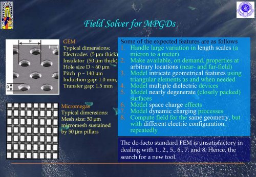
Field Solver for MPGDs<br />
GEM<br />
Typical dimensions:<br />
Electrodes (5 μm thick)<br />
Insulator (50 μm thick)<br />
Hole size D ~ 60 μm<br />
Pitch p ~ 140 μm<br />
Induction gap: 1.0 mm,<br />
Transfer gap: 1.5 mm<br />
Micromegas<br />
Typical dimensions:<br />
Mesh size: 50 μm<br />
micromesh sustained<br />
by 50 μm pillars<br />
Some <strong>of</strong> the expected features are as follows<br />
1. Handle large variation in length scales (a<br />
micron to a meter)<br />
2. Make available, on demand, properties at<br />
arbitrary locations (near- and far-field)<br />
3. Model intricate geometrical features using<br />
triangular elements as and when needed<br />
4. Model multiple dielectric devices<br />
5. Model nearly degenerate (closely packed)<br />
surfaces<br />
6. Model space charge effects<br />
7. Model dynamic charging processes<br />
8. Compute field for the same geometry, but<br />
with different electric configuration,<br />
repeatedly<br />
The de‐facto standard FEM is unsatisfactory in<br />
dealing with 1., 2., 5., 6., 7. and 8. Hence, the<br />
search for a new tool.
Field Solver<br />
Solution <strong>of</strong> 3D Poisson's Equation using a recently proposed BEM - neBEM<br />
• Numerical implementation <strong>of</strong> boundary integral equations (BIE) based on Green’s<br />
function by discretization <strong>of</strong> boundary.<br />
• Boundary elements endowed with distribution <strong>of</strong> sources, doublets, dipoles, vortices.<br />
Potential at r<br />
Electrostatics BIE<br />
Φ( r)<br />
= ∫ G(<br />
r,<br />
r′<br />
) ρ ( r′<br />
) dS ′<br />
S<br />
Green’s function<br />
G ( r , r ′)<br />
=<br />
4 πε<br />
1<br />
r<br />
−<br />
r<br />
′<br />
Charge density at r’<br />
Influence<br />
Coefficient<br />
Matrix<br />
discretization<br />
[ A]{ ρ} = { Φ}<br />
{ρ} = [A] -1 {Φ}<br />
ε - permittivity <strong>of</strong> medium<br />
Accuracy depends critically on the<br />
estimation <strong>of</strong> [A], in turn, the<br />
integration <strong>of</strong> G, which involves<br />
singularities when r → r'.<br />
Most conventional BEM solvers fail<br />
here leading to large numerical errors.
Contrast <strong>of</strong> approaches<br />
Conventional BEM (nodal) versus nearly exact BEM (distributed)<br />
We have derived exact expressions for<br />
the integration <strong>of</strong> G and its derivative<br />
for uniform charge distributions over<br />
triangular and rectangular elements<br />
Conventionally, charges are assumed to be<br />
concentrated at nodes. This is convenient<br />
since the preceding integration is avoided.<br />
Introduces large errors in the near field.
Micromegas<br />
Electrostatics <strong>of</strong> MPGDs<br />
Micro‐Wire<br />
200<br />
180<br />
160<br />
neBEM<br />
FEM<br />
Theoretical considerations<br />
imply better performance by<br />
the neBEM solver which<br />
solves for the charge density<br />
on boundary elements rather<br />
than potential at a pre‐fixed<br />
set <strong>of</strong> nodal points.<br />
140<br />
E (kV/cm)<br />
140<br />
120<br />
100<br />
80<br />
60<br />
40<br />
20<br />
0<br />
20 40 60 80 100 120 140<br />
Y (µm)<br />
FEM: gap = 32µm<br />
gap = 40µm<br />
gap = 65µm<br />
gap = 75µm<br />
gap = 85µm<br />
neBEM: gap = 32µm<br />
gap = 40µm<br />
gap = 65µm<br />
gap = 75µm<br />
gap = 85µm<br />
E (kV/cm)<br />
Total E field (kV/cm)<br />
120<br />
100<br />
80<br />
60<br />
40<br />
20<br />
0<br />
-100 0 100 200 300 400 500 600 700<br />
Y (µm)<br />
300<br />
280<br />
260<br />
240<br />
220<br />
200<br />
180<br />
160<br />
140<br />
120<br />
100<br />
80<br />
neBEM Segmented<br />
FEM Segmented<br />
neBEM Mesh<br />
FEM Mesh<br />
60<br />
0 100 200 300 400 500 600<br />
Distance * 10 micron<br />
Numerical comparisons<br />
1) neBEM results are as<br />
accurate as FEM results in the<br />
far‐field<br />
2) In the near‐field, neBEM<br />
performs better than FEM<br />
3) No artificial truncation <strong>of</strong><br />
open domain is necessary<br />
while using neBEM
Plans for the near future<br />
‣ Development <strong>of</strong> an interface to ROOT so that devices built using ROOT<br />
can be directly imported to neBEM and solved for<br />
‣ Study dynamic charging<br />
‣ Improve upon Particles‐on‐Surface – a model to represent space charge<br />
‣ Simulate problems related to magnetostatics<br />
‣ A working interface to garfield and the new detailed detector simulation<br />
framework is expected to be complete by the middle <strong>of</strong> 2009<br />
‣ We will also try to set up an experimental laboratory for the development<br />
<strong>of</strong> MPGD as soon as possible<br />
Supratik Mukhopadhay, Nayana Majumdar, Sudeb Bhattacharya<br />
<strong>Saha</strong> <strong>Institute</strong> <strong>of</strong> <strong>Nuclear</strong> <strong>Physics</strong>, Kolkata, India<br />
E‐mails: supratik.mukhopadhyay@saha.ac.in, nayana.majumdar@saha.ac.in, sudeb.bhattacharya@saha.ac.in