0201 Chip Component Design and Assembly Issues
0201 Chip Component Design and Assembly Issues
0201 Chip Component Design and Assembly Issues
You also want an ePaper? Increase the reach of your titles
YUMPU automatically turns print PDFs into web optimized ePapers that Google loves.
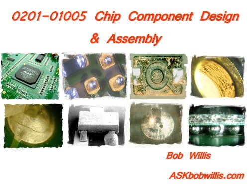
<strong>0201</strong>-01005 <strong>Chip</strong> <strong>Component</strong> <strong>Design</strong><br />
& <strong>Assembly</strong><br />
Bob Willis<br />
ASKbobwillis.com
Edited by Bob Willis – 2002 for the Red Cross 9/11 Fund
0.010” (250um)<br />
0.020” (500um)<br />
0.010” (250um)
<strong>Component</strong> Placement 01005<br />
Assembleon
Productronica <strong>0201</strong> Test Board<br />
0.012” (0.30mm)<br />
0.016” (0.42mm)<br />
0.007” (0.18mm)
01005 <strong>Chip</strong> <strong>Component</strong> <strong>Assembly</strong><br />
0.007” (0.180mm)<br />
0.011” (0.280mm)<br />
0.006” (0.160mm)
Printed Board Layout<br />
St<strong>and</strong>ard pad <strong>and</strong> solder mask layout can be used
Printed Board Layout<br />
Solder mask block aperture is recommended with no mask between pads. Some engineers<br />
have suggested using mask defined pads which has not been found to be beneficial. Images<br />
shows pads after printing <strong>and</strong> reflow
Solder Mask Defined Pads
Printed Board Layout<br />
0.006”<br />
0.150um<br />
The component separation will decrease but will be limited by PCB fabrication issues rather<br />
than placement or design layout
Printed Board Layout<br />
Direction of component placement does not have an impact on reflow based<br />
on trials with convection or vapour phase reflow
Printed Board Layout Via-in-Pad
LGA/QFN Via Hole Options
Printed Board Layout Via-in-Pad<br />
Mobile phone application with blind, stacked vias with resist defined pads <strong>and</strong> fillet less joints the<br />
photographs are taken from microsections as part of a product teardown
Printed Board Layout Via-in-Pad<br />
Open via design which is poor practice when using via in pad the visible voids in the x-ray<br />
are the result of the open vias
<strong>Component</strong> Lift & Tombstoning<br />
Video simulation on NPI design trials <strong>and</strong> defect investigations
Solder Paste Stencil <strong>Design</strong><br />
Laser cut stencil<br />
0.005”/125um stainless steel<br />
0.006”/150um stainless steel<br />
Electroform<br />
0.004”/100um nickel provided the best<br />
results with a type 4 powder<br />
Stencil aperture size for size with pads with<br />
rounded corners for better paste release
Printed Board Layout<br />
If you still see solder beads after reflow you can change the stencils aperture width reducing<br />
the paste under the body of the component, the main reason is poor pad design
Printed Board Layout<br />
Although changing the stencil overcomes production problem its better to correct the<br />
cause, otherwise the design defect then is recreated on future designs
Printing <strong>0201</strong> Solder Paste Video<br />
Video shows paste being printed on to a<br />
glass surface through stencil apertures
<strong>0201</strong>/01005 <strong>Component</strong> Placement <strong>Issues</strong><br />
Special pick up tools<br />
Inconsistent packaging<br />
<strong>Component</strong> size variation<br />
Static electricity charges/cover tape<br />
<strong>Component</strong> contingence requirements
<strong>0201</strong> <strong>Component</strong> Placement<br />
Assembleon
<strong>Chip</strong> <strong>Component</strong> Static Pick Up
Harting Fair Production Line<br />
Example production line set up to demonstrate lead-free assembly with complete component range,<br />
including 01005 <strong>and</strong> intrusive reflow connectors
PIHR <strong>Component</strong> Placement
PIH <strong>Component</strong> Placement
Printing PIHR Solder Paste Video
Printing Solder Paste
Printing Solder Paste Alignment <strong>Issues</strong>
Convection Reflow Soldering<br />
Maximum Temperature Recorded 247 o C<br />
Temperature Differential DT 17 o C
Lead-Free Vapour Phase Soldering<br />
Maximum Temperature Recorded 233 o C<br />
Temperature Differential DT 3 o C
Reflow Soldering 01005 with Lead-Free Paste<br />
<strong>Chip</strong> Resistors<br />
<strong>Chip</strong> Capacitors
X-Ray Images of 01005 <strong>Chip</strong> Joints<br />
X-ray images of capacitors <strong>and</strong> a resistor after convection reflow in air
Process Defects - Billboards
01005 <strong>Chip</strong> <strong>Component</strong> <strong>Assembly</strong>
<strong>0201</strong> Rework <strong>and</strong> Repair
01005 Rework <strong>and</strong> Repair<br />
Video Clip showing rework of 01005
01005 <strong>Chip</strong> <strong>Component</strong> Tape<br />
New St<strong>and</strong>ards Required<br />
B<br />
D<br />
A<br />
F<br />
H<br />
A B D F H<br />
Metric +/-0.0 +/-0.0 +/- 0.0 +/- 0.0 +/-0.0
01005 Filletless <strong>Assembly</strong> <strong>Design</strong> Size<br />
0.004” (0.10mm)<br />
0.005” (0.12mm)<br />
0.009” (0.29mm) 0.007” (0.18mm)<br />
0.006” (0.15mm) 0.008” (0.20mm)<br />
New pad sizes, No real volume production trail results available yet!!<br />
Actual pad size on manufactured panels as measured
<strong>0201</strong> - 01005 Filletless <strong>Assembly</strong> <strong>Design</strong><br />
With this type of footprint there is no fillet <strong>and</strong> the resulting joint is more like a bulbous joint<br />
one of the problems is paste contamination of the top surface of the component during<br />
placement. This then results in paste in or on the nozzle causing blockage
Convection Reflow with Lead-Free<br />
Poor coalescence of solder<br />
paste particles due to flux<br />
exhaustion on <strong>0201</strong> chip.<br />
Poor coalescence of solder paste<br />
particles due to flux exhaustion on<br />
01005 chips in air reflow.
01005 <strong>Chip</strong> <strong>Component</strong> Joints<br />
Tombstone only seen on reflow video<br />
simulations not on production, so far!!
Throughput capability for the highest<br />
thermal dem<strong>and</strong> board. Fast cooling<br />
capability with option of nitrogen<br />
System needs positive board support,<br />
measured down stop force <strong>and</strong> height<br />
control vision/pressure check on part<br />
pickup. Capability for small tape feed<br />
AOI inspection with proven capability for<br />
01005 placement, solder joint <strong>and</strong> QFN<br />
termination joints<br />
Stencil for 01005 & <strong>0201</strong> areas need to be 0.004”/100um.<br />
Solder paste particle size 4 is necessary. Printer needs to<br />
be capable of ultra fine pitch <strong>and</strong> repeatable with positive<br />
board support 3D vision or separate AOI station
Package On Package <strong>Assembly</strong>
Package on Package Microsections<br />
Microsections taken from a 14mm package
X-Ray Inspection of Joints<br />
Images of a four high package POP with larger base balls <strong>and</strong> some evidence of solder balling<br />
on the PCB. Evidence was also found on different layers of the component.<br />
AXIOM Manufacturing PoP Workshop 24 th November
Interactive & Photo CD-ROMs<br />
CDs released in 2004
Thank you!!!!<br />
Any Questions
NPL Process Defect Database<br />
http://defectsdatabase.npl.co.uk
NPL Process Defect Database
NPL Process Defect Database<br />
http://defectsdatabase.npl.co.uk
NPL Process Defect Database<br />
http://defectsdatabase.npl.co.uk
Any Questions<br />
Bob Willis<br />
ASKbobwillis.com


