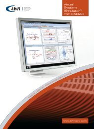
Visual System Simulator™
Visual System Simulator™
Visual System Simulator™

You also want an ePaper? Increase the reach of your titles
YUMPU automatically turns print PDFs into web optimized ePapers that Google loves.
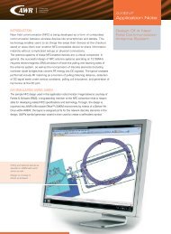
<strong>Visual</strong> <strong>System</strong><br />
Simulator<br />
(additional positioning<br />
line<br />
AXIEM<br />
here ???)<br />
White Paper<br />
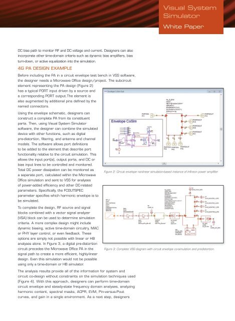
DC bias path to monitor RF and DC voltage and current. Designers can also<br />
incorporate other time-domain criteria such as dynamic bias amplifiers, bias<br />
turn-down, or active equalization into the simulation.<br />
4G PA DESIGN EXAMPLE<br />
Before including the PA in a circuit envelope test bench in VSS software,<br />
the designer needs a Microwave Office design/project. The subcircuit<br />
element representing the PA design (Figure 2)<br />
has a typical PORT input driven by a source and<br />
a corresponding PORT output.The element is<br />
also augmented by additional pins defined by the<br />
named connectors.<br />
Using the envelope schematic, designers can<br />
construct a complete PA from its constituent<br />
parts. Then, using <strong>Visual</strong> <strong>System</strong> Simulator<br />
software, the designer can combine the simulated<br />
device with other functions, such as digital<br />
pre-distortion, filtering, and antenna and channel<br />
models. The software allows port definitions<br />
to be added to the element that describe port<br />
functionality relative to the circuit simulation. This<br />
allows the input port(s), output ports, and DC or<br />
bias input lines to be controlled and monitored.<br />
Total DC power dissipation can be monitored as<br />
a separate port, calculated within the Microwave<br />
Office simulation and sent to VSS for analyses<br />
of power-added efficiency and other DC-related<br />
parameters. Specifically, the FCOUTSPEC<br />
parameter specifies which harmonic envelope is to<br />
be simulated.<br />
To complete the design, RF source and signal<br />
blocks combined with a vector signal analyzer<br />
(VSA) block can be used to determine simulation<br />
criteria. A more complex design might include<br />
dynamic biasing, active time-domain circuitry, MAC<br />
or PHY layer control, or even feedback. These<br />
options are simply not possible with linear or HB<br />
analyses alone. In Figure 3, a digital pre-distortion<br />
circuit precedes the Microwave Office PA in the<br />
signal path to create a more efficient, highly-linear<br />
design. Even this simulation would not be possible<br />
using only a time-domain or HB simulator.<br />
Figure 2: Circuit envelope nonlinear simulation-based instance of Infineon power amplifier.<br />
Figure 3: Complete VSS diagram with circuit envelope co-simulation and predistortion.<br />
The analysis results provide all of the information for system and<br />
circuit co-design without constraints on the simulation techniques used<br />
(Figure 4). With this approach, designers can perform time-domain<br />
circuit envelope and steady-state frequency domain analyses, analyzing<br />
harmonic content, spectral masks, ACPR, EVM, Pin-versus-Pout<br />
curves, and gain in a single environment. As a next step, designers