P89V51RB2/RC2/RD2 8-bit 80C51 5 V low power 16/32 ... - NetMedia
P89V51RB2/RC2/RD2 8-bit 80C51 5 V low power 16/32 ... - NetMedia
P89V51RB2/RC2/RD2 8-bit 80C51 5 V low power 16/32 ... - NetMedia

Create successful ePaper yourself
Turn your PDF publications into a flip-book with our unique Google optimized e-Paper software.
NXP Semiconductors<br />
<strong>P89V51RB2</strong>/<strong>RC2</strong>/<strong>RD2</strong><br />
8-<strong>bit</strong> microcontrollers with <strong>80C51</strong> core<br />
Table 33. WDTC - Watchdog control register (address COH) <strong>bit</strong> allocation<br />
Bit addressable; Reset value: 00H<br />
Bit 7 6 5 4 3 2 1 0<br />
Symbol - - - WDOUT WDRE WDTS WDT SWDT<br />
Table 34. WDTC - Watchdog control register (address COH) <strong>bit</strong> description<br />
Bit Symbol Description<br />
7 to 5 - Reserved for future use. Should be set to ‘0’ by user programs.<br />
4 WDOUT Watchdog output enable. When this <strong>bit</strong> and WDRE are both set, a<br />
Watchdog reset will drive the reset pin active for <strong>32</strong> clocks.<br />
3 WDRE Watchdog timer reset enable. When set enables a watchdog timer<br />
reset.<br />
2 WDTS Watchdog timer reset flag, when set indicates that a WDT reset<br />
occurred. Reset in software.<br />
1 WDT Watchdog timer refresh. Set by software to force a WDT reset.<br />
0 SWDT Start watchdog timer, when set starts the WDT. When cleared, stops<br />
the WDT.<br />
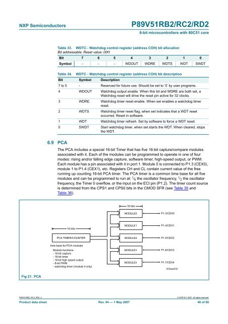
6.9 PCA<br />
The PCA includes a special <strong>16</strong>-<strong>bit</strong> Timer that has five <strong>16</strong>-<strong>bit</strong> capture/compare modules<br />
associated with it. Each of the modules can be programmed to operate in one of four<br />
modes: rising and/or falling edge capture, software timer, high-speed output, or PWM.<br />
Each module has a pin associated with it in port 1. Module 0 is connected to P1.3 (CEX0),<br />
module 1 to P1.4 (CEX1), etc. Registers CH and CL contain current value of the free<br />
running up counting <strong>16</strong>-<strong>bit</strong> PCA timer. The PCA timer is a common time base for all five<br />
modules and can be programmed to run at: 1 ⁄ 6 the oscillator frequency, 1 ⁄ 2 the oscillator<br />
frequency, the Timer 0 overf<strong>low</strong>, or the input on the ECI pin (P1.2). The timer count source<br />
is determined from the CPS1 and CPS0 <strong>bit</strong>s in the CMOD SFR (see Table 35 and<br />
Table 36).<br />
<strong>16</strong> <strong>bit</strong>s<br />
MODULE0<br />
P1.3/CEX0<br />
<strong>16</strong> <strong>bit</strong>s<br />
MODULE1<br />
P1.4/CEX1<br />
PCA TIMER/COUNTER<br />
MODULE2<br />
P1.5/CEX2<br />
time base for PCA modules<br />
Module functions:<br />
- <strong>16</strong>-<strong>bit</strong> capture<br />
- <strong>16</strong>-<strong>bit</strong> timer<br />
- <strong>16</strong>-<strong>bit</strong> high speed output<br />
- 8-<strong>bit</strong> PWM<br />
- watchdog timer (module 4 only)<br />
MODULE3<br />
MODULE4<br />
P1.6/CEX3<br />
P1.7/CEX4<br />
002aaa5<strong>32</strong><br />
Fig 21. PCA<br />
<strong>P89V51RB2</strong>_<strong>RC2</strong>_<strong>RD2</strong>_4<br />
© NXP B.V. 2007. All rights reserved.<br />
Product data sheet Rev. 04 — 1 May 2007 46 of 80