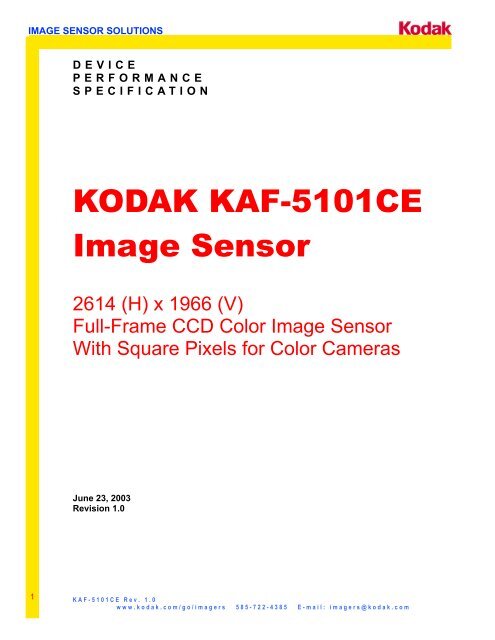
KODAK KAF-5101CE Image Sensor - digital-photography.pl
KODAK KAF-5101CE Image Sensor - digital-photography.pl
KODAK KAF-5101CE Image Sensor - digital-photography.pl

You also want an ePaper? Increase the reach of your titles
YUMPU automatically turns print PDFs into web optimized ePapers that Google loves.
IMAGE SENSOR SOLUTIONS<br />
D E V I C E<br />
P E R F O R M A N C E<br />
S P E C I F I C A T I O N<br />
<strong>KODAK</strong> <strong>KAF</strong>-<strong>5101CE</strong><br />
<strong>Image</strong> <strong>Sensor</strong><br />
2614 (H) x 1966 (V)<br />
Full-Frame CCD Color <strong>Image</strong> <strong>Sensor</strong><br />
With Square Pixels for Color Cameras<br />
June 23, 2003<br />
Revision 1.0<br />
1<br />
K A F - 5 1 0 1 C E R e v . 1 . 0<br />
w w w . k o d a k . c o m / g o / i m a g e r s 5 8 5 - 7 2 2 - 4 3 8 5 E - m a i l : i m a g e r s @ k o d a k . c o m
IMAGE SENSOR SOLUTIONS<br />
TABLE OF CONTENTS MODE OF OPERATION....................... 21<br />
Power-up Flush Cycle ....................... 21<br />
TABLE OF FIGURES .............................. 2<br />
STORAGE AND HANDLING............... 22<br />
DEVICE DESCRIPTION ..... 3 ENVIRONMENTAL CONDITIONS .............. 22<br />
HANDLING CONDITIONS ......................... 22<br />
DEVICE DESCRIPTION......................... 4 ESD.................................................... 22<br />
Soldering recommendations .............. 22<br />
ARCHITECTURE ........................................ 4<br />
Cover glass care and cleanliness ...... 23<br />
Dark Reference Pixels ......................... 4<br />
Environmental Exposure ................... 23<br />
Dark Dummy Pixels ............................ 4<br />
Dummy Pixels...................................... 5 MECHANICAL DRAWINGS ............... 24<br />
Virtual Dummy Columns ............ Error!<br />
PACKAGE ............................................... 24<br />
Bookmark not defined.<br />
GLASS TRANSMISSION............................ 26<br />
Active Buffer Pixels ............................. 5<br />
CTE Monitor Pixels..Error! Bookmark QUALITY ASSURANCE AND<br />
not defined. RELIABILITY ........................................ 27<br />
IMAGE ACQUISITION ................................ 6<br />
CHARGE TRANSPORT................................ 6 ORDERING INFORMATION .............. 28<br />
HORIZONTAL REGISTER ........................... 7<br />
AVAILABLE PART CONFIGURATIONS...... 28<br />
Output Structure .................................. 7<br />
REVISION CHANGES .......................... 29<br />
Output Load......................................... 8<br />
PHYSICAL DESCRIPTION ........................... 9<br />
Pin Description and Device TABLE OF FIGURES<br />
Figure 1 - <strong>Sensor</strong> Architecture .............................................. 4<br />
Orientation .......................................... 9<br />
Figure 2 - Output Architecture .............................................. 7<br />
Figure 3 – Recommended Output Structure Load Diagram . 8<br />
PERFORMANCE ................................... 10 Figure 4 – Package Pin Description ..................................... 9<br />
Figure 5 – Estimated Quantum Efficiency .......................... 12<br />
<strong>Image</strong> Performance Operational Figure 6 – Typical Angular Response................................. 12<br />
Conditions ......................................... 10 Figure 7 – Typical Blooming Performance.......................... 13<br />
Figure 8 - Frame Timing ..................................................... 18<br />
Imaging Performance Specifications 10 Figure 9 - Line Timing and content ..................................... 19<br />
Typical Performance Curves............. 12 Figure 10 – Pixel Timing ..................................................... 20<br />
Figure 11 – Power-up Flush Cycle ..................................... 21<br />
DEFECT DEFINITIONS ............................. 14 Figure 12 - Package Drawing ............................................. 25<br />
Defect Operational Conditions ......... 14 Figure 13 - Glass Transmission .......................................... 26<br />
Defect Specifications ......................... 14<br />
OPERATION........................................... 15<br />
ABSOLUTE MAXIMUM RATINGS............. 15<br />
Power-up Sequence ........................... 15<br />
DC BIAS OPERATING CONDITIONS ........ 16<br />
AC OPERATING CONDITIONS ................. 16<br />
Clock Levels ...................................... 16<br />
Timing Requirements......................... 17<br />
TIMING DIAGRAMS ............................ 18<br />
Frame Timing .................................... 18<br />
Line Timing ....................................... 19<br />
Pixel Timing ...................................... 20<br />
2<br />
K A F - 5 1 0 1 C E R e v . 1 . 0<br />
w w w . k o d a k . c o m / g o / i m a g e r s 5 8 5 - 7 2 2 - 4 3 8 5 E - m a i l : i m a g e r s @ k o d a k . c o m
IMAGE SENSOR SOLUTIONS<br />
S U M M A R Y S P E C I F I C A T I O N<br />
<strong>KODAK</strong> <strong>KAF</strong>-<strong>5101CE</strong> <strong>Image</strong> <strong>Sensor</strong><br />
2614 (H) x 1966 (V) Full-Frame CCD<br />
Color <strong>Image</strong> <strong>Sensor</strong><br />
Parameter Typical Value<br />
Full Frame CCD; with<br />
Architecture<br />
Square Pixels<br />
2738 (H) x 2044 (V) =<br />
Total Number of Pixels<br />
5.60M<br />
Number of Effective 2654 (H) x 2006 (V) =<br />
Pixels 5.32M<br />
2614 (H) x 1966 (V) =<br />
Number of Active Pixels<br />
5.14M<br />
Pixel Size 6.8µm (H) x 6.8µm (V)<br />
<strong>Image</strong>r Size 22.3mm (diagonal)<br />
19.7mm (H) x<br />
Chip Size<br />
15.04mm (V)<br />
Aspect Ratio 4:3<br />
-<br />
Description Saturation Signal 40K e<br />
The <strong>KAF</strong>-<strong>5101CE</strong> is a 22.3mm diagonal (Type 4/3)<br />
Quantum Efficiency<br />
high performance color full-frame CCD (charge- 0.31, 0.34, 0.31<br />
(RGB)<br />
cou<strong>pl</strong>ed device) image sensor designed for a wide<br />
-<br />
range of color image sensing ap<strong>pl</strong>ications including Total <strong>Sensor</strong> Noise 17 e<br />
<strong>digital</strong> imaging. Each pixel contains blooming<br />
Dark Signal 5 mV/s<br />
protection by means of a lateral overflow drain<br />
thereby preventing image corruption during high Dark Current Doubling<br />
6.3 °C<br />
light level conditions. Each of the 6.8µm square Temperature<br />
pixels are patterned with an RGB mosaic color filter<br />
Linear Dynamic Range 67 dB<br />
with overlying microlenses for improved color<br />
response and reproduction. A border of buffer and Charge Transfer<br />
0.999995<br />
light-shielded pixels surrounds the photoactive Efficiency<br />
pixels.<br />
Blooming Protection 1500x saturation<br />
@4ms integration time exposure<br />
All parameters above are specified at T = 60ºC and a data rate of 28MHz<br />
Maximum Data Rate 28 MHz<br />
REVISION NO.: 1.0<br />
EFFECTIVE DATE: June 23, 2003<br />
3<br />
K A F - 5 1 0 1 C E R e v . 1 . 0<br />
w w w . k o d a k . c o m / g o / i m a g e r s 5 8 5 - 7 2 2 - 4 3 8 5 E - m a i l : i m a g e r s @ k o d a k . c o m
IMAGE SENSOR SOLUTIONS<br />
DEVICE DESCRIPTION<br />
Architecture<br />
Color Fill Pattern 1 Active (CTE Monitor)<br />
3 Dark Dummy<br />
GR r R GR r 20 Active Buffer<br />
924 pixels V1<br />
B GB r B<br />
V2<br />
GR r R GR r<br />
<strong>KAF</strong>-<strong>5101CE</strong><br />
Usable Active <strong>Image</strong> Area<br />
196 pixels 2614 (H) x 1966 (V)<br />
6.8 microns x 6.8 microns pixels<br />
4:3 Aspect Ratio<br />
1966 Active Lines/Frame<br />
924 pixels<br />
LODT<br />
H1L<br />
LODB<br />
RD 20 Active Buffer<br />
6 Dark Dummy<br />
RG 23 Dark<br />
5 Dark Dummy<br />
VDD Last Hccd Phase: H1 Last Vccd Phase: V2<br />
VOUT 2614 Active Pixels/Line H1<br />
(typical active line format) H2<br />
VSS<br />
20 Active Buffer 6 Dark Dummy 20 Active Buffer<br />
SUB 4 Dark Dummy 31 Dark<br />
23 Dummy 5 Dark Dummy 2 Dummy<br />
OG 1 Active (CTE Monitor) 1 Active (CTE Monitor)<br />
6 Dummy 2 Dummy<br />
3 Virtual Dummy Column<br />
Figure 1 - <strong>Sensor</strong> Architecture<br />
Dark Reference Pixels<br />
Surrounding the periphery of the device is a line. There are also 23 full dark lines at the start of<br />
border of light shielded pixels creating a dark every frame. Under normal circumstances, these<br />
region. Within this dark region, exist light shielded pixels do not respond to light and may be used as<br />
pixels that include 31 trailing dark pixels on every a dark reference.<br />
Dark Dummy Pixels<br />
Within the dark region some pixels are in close Within the dark region, dark dummy pixels have<br />
proximity to an active pixel, or the light sensitive been identified. There are 4 leading and 11 (5 + 6)<br />
regions that have been added for manufacturing trailing dark pixels on every line. There are also<br />
test purposes, (CTE Monitor). In both cases, these 11 (5 + 6) dark dummy lines at the start of every<br />
pixels can scavenge signal depending on light frame along with 3 dark dummy lines at the end of<br />
intensity and wavelength. These pixels should not each frame.<br />
be used as a dark reference. These pixels are<br />
called dark dummy pixels.<br />
4<br />
K A F - 5 1 0 1 C E R e v . 1 . 0<br />
w w w . k o d a k . c o m / g o / i m a g e r s 5 8 5 - 7 2 2 - 4 3 8 5 E - m a i l : i m a g e r s @ k o d a k . c o m
IMAGE SENSOR SOLUTIONS<br />
Dummy Pixels<br />
Within the horizontal shift register there are 29, shift register dark current signal and do not<br />
(6 + 23), leading and 4, (2 + 2), trailing additional respond to light and therefore, have been<br />
shift phases that are not electrically associated designated as dummy pixels. For this reason,<br />
with any columns of pixels within the vertical they should not be used to determine a dark<br />
register. These pixels contain only horizontal reference level.<br />
Virtual Dummy Columns<br />
Within the horizontal shift register there is three to light and therefore, have been designated as<br />
leading shift phases that are not physically virtual dummy columns. For this reason they<br />
associated with a column of pixels within the also should not be used to determine dark<br />
vertical register. These pixels contain only reference level.<br />
horizontal shift register dark current and do not<br />
Active Buffer Pixels<br />
Twenty unshielded pixels adjacent to any are light sensitive but they are not tested for<br />
leading or trailing dark reference regions are defects and non-uniformities.<br />
classified as active buffer pixels. These pixels<br />
CTE Monitor Pixel<br />
Within the horizontal dummy pixel region two monitor pixels are used for manufacturing test<br />
light sensitive test pixels (one each on the purposes. In order to facilitate measuring the<br />
leading and trailing ends) are added and within device CTE, the pixels in the CTE Monitor<br />
the vertical dummy pixel region one light region may be coated with red and blue pigment<br />
sensitive test pixel has been added. These CTE or may be covered with a light shielding metal.<br />
5<br />
K A F - 5 1 0 1 C E R e v . 1 . 0<br />
w w w . k o d a k . c o m / g o / i m a g e r s 5 8 5 - 7 2 2 - 4 3 8 5 E - m a i l : i m a g e r s @ k o d a k . c o m
IMAGE SENSOR SOLUTIONS<br />
<strong>Image</strong> Acquisition<br />
An electronic representation of an image is When the pixel's capacity is reached, excess<br />
formed when incident photons falling on the electrons are discharged into the lateral overflow<br />
sensor <strong>pl</strong>ane create electron-hole pairs within drain to prevent crosstalk or ‘blooming’. During<br />
the device. These photon-induced electrons are the integration period, the V1 and V2 register<br />
collected locally by the formation of potential clocks are held at a constant (low) level.<br />
wells at each photogate or pixel site. The<br />
number of electrons collected is linearly<br />
dependent on light level and exposure time and<br />
non-linearly dependent on wavelength.<br />
Charge Transport<br />
The integrated charge from each photogate is each line, pixel by pixel, to the output structure<br />
transported to the output using a two-step by alternately clocking the H1 and H2 pins in a<br />
process. Each line (row) of charge is first com<strong>pl</strong>ementary fashion. A separate connection<br />
transported from the vertical CCD’s to a to the last H1 phase (H1L) is provided to<br />
horizontal CCD register using the V1 and V2 improve the transfer speed of charge to the<br />
register clocks. The horizontal CCD is presented floating diffusion. On each falling edge of H1 a<br />
a new line on the falling edge of V2 while H1 is new charge packet is dumped onto a floating<br />
held high. The horizontal CCD’s then transport diffusion and sensed by the output am<strong>pl</strong>ifier.<br />
6<br />
K A F - 5 1 0 1 C E R e v . 1 . 0<br />
w w w . k o d a k . c o m / g o / i m a g e r s 5 8 5 - 7 2 2 - 4 3 8 5 E - m a i l : i m a g e r s @ k o d a k . c o m
IMAGE SENSOR SOLUTIONS<br />
Horizontal Register<br />
Output Structure<br />
H2<br />
HCCD<br />
Charge<br />
H1<br />
Transfer<br />
VDD<br />
H1L<br />
OG<br />
RG<br />
RD<br />
Floating<br />
Diffusion VOUT<br />
VSS<br />
Source Source Source<br />
Follower Follower Follower<br />
#1 #2 #3<br />
Figure 2 - Output Architecture<br />
Charge presented to the floating diffusion (FD) is remove the signal and FD is reset to the potential<br />
converted into a voltage and is current am<strong>pl</strong>ified in ap<strong>pl</strong>ied by reset drain (RD). Increased signal at<br />
order to drive off-chip loads. The resulting voltage the floating diffusion reduces the voltage seen at<br />
change seen at the output is linearly related to the the output pin. To activate the output structure, an<br />
amount of charge <strong>pl</strong>aced on the FD. Once the off-chip load must be added to the VOUT pin of<br />
signal has been sam<strong>pl</strong>ed by the system the device. See Figure 3.<br />
electronics, the reset gate ( RG ) is clocked to<br />
7<br />
K A F - 5 1 0 1 C E R e v . 1 . 0<br />
w w w . k o d a k . c o m / g o / i m a g e r s 5 8 5 - 7 2 2 - 4 3 8 5 E - m a i l : i m a g e r s @ k o d a k . c o m
IMAGE SENSOR SOLUTIONS<br />
Output Load<br />
VDD = +15V<br />
Iout = 5.4mA<br />
0.1uF<br />
VOUT<br />
2N3904<br />
or Equiv.<br />
130 Ohms Buffered<br />
Video<br />
Output<br />
680 Ohms<br />
Figure 3 – Recommended Output Structure Load Diagram<br />
Component values may be revised based on operating conditions and other design considerations.<br />
8<br />
K A F - 5 1 0 1 C E R e v . 1 . 0<br />
w w w . k o d a k . c o m / g o / i m a g e r s 5 8 5 - 7 2 2 - 4 3 8 5 E - m a i l : i m a g e r s @ k o d a k . c o m
IMAGE SENSOR SOLUTIONS<br />
Physical Description<br />
Pin Description and Device Orientation<br />
Pin 1 Indicator<br />
SUB 1 32 N/C<br />
OG LODT<br />
RG V1<br />
RD V1<br />
RD V2<br />
VSS V2<br />
VOUT SUB<br />
VDD N/C<br />
SUB V2<br />
H1L V2<br />
N/C V1<br />
SUB V1<br />
H1 SUB<br />
H1 N/C<br />
H2 N/C<br />
H2 16 17 LODB<br />
Pin Name Description Pin Name Description<br />
1 SUB Substrate 32 N/C No Connection<br />
2 OG Output Gate 31 LODT Lateral Overflow Drain Top<br />
3 RG Reset Gate 30 V1 Vertical Phase 1<br />
4 RD Reset Drain Bias 29 V1 Vertical Phase 1<br />
5 RD Reset Drain Bias 28 V2 Vertical Phase 2<br />
6 VSS Output Am<strong>pl</strong>ifier Return 27 V2 Vertical Phase 2<br />
7 VOUT Output 26 SUB Substrate<br />
8 VDD Output Am<strong>pl</strong>ifier Sup<strong>pl</strong>y 25 N/C No Connection<br />
9 SUB Substrate 24 V2 Vertical Phase 2<br />
10 H1L Horizontal Phase 1, Last Gate 23 V2 Vertical Phase 2<br />
11 N/C No Connection 22 V1 Vertical Phase 1<br />
12 SUB Substrate 21 V1 Vertical Phase 1<br />
13 H1 Horizontal Phase 1 20 SUB Substrate<br />
14 H1 Horizontal Phase 1 19 N/C No Connection<br />
15 H2 Horizontal Phase 2 18 N/C No Connection<br />
16 H2 Horizontal Phase 2 17 LODB Lateral Overflow Drain Bottom<br />
Figure 4 – Package Pin Description<br />
9<br />
K A F - 5 1 0 1 C E R e v . 1 . 0<br />
w w w . k o d a k . c o m / g o / i m a g e r s 5 8 5 - 7 2 2 - 4 3 8 5 E - m a i l : i m a g e r s @ k o d a k . c o m
IMAGE SENSOR SOLUTIONS<br />
PERFORMANCE<br />
<strong>Image</strong> Performance Operational Conditions<br />
Description Condition - Unless otherwise noted Notes<br />
Frame time (t readout ) 289.05 msec Includes overclock pixels<br />
Integration time (t int ) 33 msec<br />
Horizontal clock<br />
28 MHz<br />
frequency<br />
Temperature 60°C Except where noted<br />
Mode Flush - integrate – readout cycle<br />
Imaging Performance Specifications<br />
Sam<strong>pl</strong>e<br />
Description Symbol Min. Nom. Max. Units Notes 16<br />
Plan<br />
Saturation Signal Vsat 540 720 mV 1 die<br />
- -<br />
Linear Saturation Signal Ne sat 40K e 1 design<br />
Quantum red, QE r 31 die<br />
Effeciency green, QE g 34 % 3 die<br />
blue QE b 31 die<br />
Photo Response Non-<br />
PRNL 15 % 2 die<br />
Linearity<br />
Photo Response Non-<br />
PRNU 8 15 %p-p 3 die<br />
Uniformity<br />
Dark Signal DarkSig 3 40 mV/s 4 die<br />
Dark Signal Non-<br />
DSNU 0.3 5 mV p-p 5 die<br />
Uniformity<br />
Dark Signal Doubling<br />
∆T 6.3 °C design<br />
Temperature<br />
-<br />
23 62 e rms<br />
Total Noise Dfld_noi 6 die<br />
0.40 1.08 mV<br />
-<br />
Total <strong>Sensor</strong> Noise N 17 e rms 15 design<br />
Linear Dynamic Range DR 67 dB 7 design<br />
Hue Shift HueUnif 4 15 % 8 die<br />
Horizontal Charge<br />
HCTE 0.999990 0.999995 9 die<br />
Transfer Efficiency<br />
Blooming Protection X_b 750 1500 x Esat 10 design<br />
DC Offset, output<br />
Vodc 6.5 7.9 9 V 11 die<br />
am<strong>pl</strong>ifier<br />
10<br />
K A F - 5 1 0 1 C E R e v . 1 . 0<br />
w w w . k o d a k . c o m / g o / i m a g e r s 5 8 5 - 7 2 2 - 4 3 8 5 E - m a i l : i m a g e r s @ k o d a k . c o m
IMAGE SENSOR SOLUTIONS<br />
Sam<strong>pl</strong>e<br />
Description Symbol Min. Nom. Max. Units Notes 16<br />
Plan<br />
Output Am<strong>pl</strong>ifier<br />
f -3dB 100 116 132 Mhz 12 die<br />
Bandwidth<br />
Output Impedance,<br />
R OUT 120 135 150 Ohms die<br />
Am<strong>pl</strong>ifier<br />
Hclk Feedthru V hft 0 42 90 mV 13 die<br />
Reset Feedthru V rft 500 810 1000 mV 14 design<br />
Notes:<br />
1. Increasing output load currents to improve bandwidth will decrease these values.<br />
2. Worst case deviation, (from 10mV to Vsat min), relative to a linear fit ap<strong>pl</strong>ied between 0 and 500mV<br />
exposure. Specified at 25°C.<br />
3. Peak to peak non-uniformity test based on an average of 147 x 147 blocks.<br />
4. Average non-illuminated signal with respect to over clocked horizontal register signal.<br />
5. Absolute difference between the maximum and minimum average signal levels of 146 x 146 blocks within<br />
the sensor.<br />
6. Dark rms deviation of a multi-sam<strong>pl</strong>ed pixel as measured using the <strong>KAF</strong>-<strong>5101CE</strong> Evaluation Board.<br />
7. 20log(Vsat/N)<br />
8. Gradual variations in hue (red with respect to green pixels and blue with respect to green pixels) in<br />
regions of interest of 147 x 147 blocks.<br />
9. Measured per transfer at 80% of Vsat.<br />
10. Esat equals the exposure required to achieve saturation. X_b represents the number of Esat exposures<br />
the sensor can tolerate before failure. Specified at 4 msec.<br />
11. Video level DC offset with respect to ground at clamp position.<br />
12. Last stage only. CLOAD = 10pF. Then f -3dB = ( 1 / (2π*ROUT*CLOAD) ).<br />
13. Amount of artificial signal due to H1 cou<strong>pl</strong>ing.<br />
14. Am<strong>pl</strong>itude of feedthrough pulse in VOUT due to RG cou<strong>pl</strong>ing.<br />
15. Calculated value subtracting the noise contribution from the <strong>KAF</strong>-<strong>5101CE</strong> Evaluation Board as 15<br />
electrons rms.<br />
16. Sam<strong>pl</strong>ing <strong>pl</strong>an defined as “die” indicates that every device is verified against the specified performance<br />
limits. Sam<strong>pl</strong>ing <strong>pl</strong>an defined as “design” indicates a sam<strong>pl</strong>ed test or characterization, at the discretion of<br />
Kodak, against the specified performance limits.<br />
11<br />
K A F - 5 1 0 1 C E R e v . 1 . 0<br />
w w w . k o d a k . c o m / g o / i m a g e r s 5 8 5 - 7 2 2 - 4 3 8 5 E - m a i l : i m a g e r s @ k o d a k . c o m
IMAGE SENSOR SOLUTIONS<br />
Typical Performance Curves<br />
<strong>KAF</strong>-<strong>5101CE</strong>: Absolute Quantum Efficiency With Clear Cover Glass<br />
0.40<br />
0.35 R GRr GBr B<br />
0.30<br />
0.25<br />
0.20<br />
QE (Absolute) 0.15<br />
0.10<br />
0.05<br />
0.00<br />
200 300 400 500 600 700 800 900 1000 1100<br />
Wavelength (nm)<br />
Figure 5 – Estimated Quantum Efficiency<br />
1.1<br />
1<br />
0.9<br />
0.8<br />
0.7<br />
0.6<br />
0.5<br />
0.4<br />
Normalized Response<br />
0.3<br />
0.2<br />
0.1 Vertical Horizontal<br />
-25 -20 -15 -10 -5 0 5 10 15 20 25<br />
Angle<br />
Figure 6 – Typical Angular Response<br />
12<br />
K A F - 5 1 0 1 C E R e v . 1 . 0<br />
w w w . k o d a k . c o m / g o / i m a g e r s 5 8 5 - 7 2 2 - 4 3 8 5 E - m a i l : i m a g e r s @ k o d a k . c o m
IMAGE SENSOR SOLUTIONS<br />
4000<br />
3500<br />
3000<br />
2500<br />
2000<br />
1500<br />
1000<br />
Blooming Protection (X_b) 500<br />
0 1 2 3<br />
Exposure Time (msec)<br />
Figure 7 – Typical Blooming Performance<br />
13<br />
K A F - 5 1 0 1 C E R e v . 1 . 0<br />
w w w . k o d a k . c o m / g o / i m a g e r s 5 8 5 - 7 2 2 - 4 3 8 5 E - m a i l : i m a g e r s @ k o d a k . c o m
IMAGE SENSOR SOLUTIONS<br />
Defect Definitions<br />
Defect Operational Conditions<br />
o<br />
All defect tests performed at T=25 C, t int = 33 msec and t readout = 289.05 msec<br />
Defect Specifications<br />
Classification Points Clusters Columns<br />
Standard Quality (SQ)
IMAGE SENSOR SOLUTIONS<br />
OPERATION<br />
Absolute Maximum Ratings<br />
9<br />
Description Symbol Minimum Maximum Units Notes<br />
Diode Pin Voltages V diode -0.6 16.5 V 1,2<br />
Gate Pin Voltages V gate1 -16.5 16.5 V 1,3<br />
Overlapping Gate Voltages V 1-2 -16.5 16.5 V 4<br />
Non-overlapping Gate Voltages V g-g -16.5 16.5 V 5<br />
V1, V2 – LOD Voltages V V-L -17 21.5 V 6<br />
Output Bias Current I out -30 mA 7<br />
LOD Diode Voltage V LOD -0.5 16 V 8<br />
Notes:<br />
1. Referenced to pin SUB<br />
2. Includes pins: RD, VDD, VSS, VOUT.<br />
3. Includes pins: V1, V2, H1, H1L , H2, RG, OG.<br />
4. Voltage difference between overlapping gates. Includes: V1 to V2; H1, H1L to H2; H1L to OG; V1 to<br />
H2.<br />
5. Voltage difference between non-overlapping gates. Includes: V1 to H1, H1L; V2, OG to H2.<br />
6. Voltage difference between V1 and V2 gates and LODT, LODB diode.<br />
7. Avoid shorting output pins to ground or any low impedance source during operation. Am<strong>pl</strong>ifier<br />
bandwidth increases at higher currents and lower load capacitance at the expense of reduced gain<br />
(sensitivity). Operation at these values will reduce MTTF.<br />
8. V1, H1, V2, H2, H1L, OG, and RD are tied to 0V.<br />
9. Absolute maximum rating is defined as a level or condition that should not be exceeded at any time<br />
per the description. If the level or condition is exceeded, the device will be degraded and may be<br />
damaged.<br />
Power-up Sequence<br />
The sequence chosen to perform an initial power-up is not critical for device reliability. A coordinated<br />
sequence may minimize noise and the following sequence is recommended:<br />
1. Connect the ground pins (SUB).<br />
2. Sup<strong>pl</strong>y the appropriate biases and clocks to the remaining pins.<br />
15<br />
K A F - 5 1 0 1 C E R e v . 1 . 0<br />
w w w . k o d a k . c o m / g o / i m a g e r s 5 8 5 - 7 2 2 - 4 3 8 5 E - m a i l : i m a g e r s @ k o d a k . c o m
IMAGE SENSOR SOLUTIONS<br />
DC Bias Operating Conditions<br />
Maximum DC<br />
Description Symbol Minimum Nominal Maximum Units Notes<br />
Current (mA)<br />
Reset Drain RD 11.3 11.5 11.7 V I RD = 0.01<br />
Output Am<strong>pl</strong>ifier Return VSS 1.05 1.25 1.45 V I SS = -3.0<br />
Output Am<strong>pl</strong>ifier Sup<strong>pl</strong>y VDD 14.5 15.0 15.5 V I OUT + I SS<br />
Substrate SUB GND V -0.01 2<br />
Output Gate OG 1.05 1.25 1.45 V 0.1<br />
Lateral Drain LODT, LODB 9.5 10.0 10.5 V 0.2 2<br />
Video Output Current I OUT -3 -5 -8 mA 1<br />
Notes:<br />
1. An output load sink must be ap<strong>pl</strong>ied to VOUT to activate output am<strong>pl</strong>ifier - see Figure 3.<br />
2. Maximum current expected up to saturation exposure (Esat).<br />
AC Operating Conditions<br />
Clock Levels<br />
Effective<br />
Description Symbol Level Minimum Nominal Maximum Units Notes<br />
Capacitance<br />
V1 Low Level V1L Low -9.5 -9.0 -8.5 V 116 nF 1<br />
V1 High Level V1H High 1.5 2 2.5 V 1<br />
V2 Low Level V2L Low -9.5 -9.0 -8.5 V 116nF 1<br />
V2 High Level V2H High 1.5 2 2.5 V 1<br />
RG, H1, H2, am<strong>pl</strong>itude RG amp RG = 7pF<br />
H1 amp Amp 5.5 6.0 6.5 V H1 = 202pF 1<br />
H2 amp H2 = 109pF<br />
H1L, am<strong>pl</strong>itude H1L amp , Amp 7.5 8.0 8.5 V 10pF 1<br />
H1 Low Level H1 low, Low -4.7 -4.5 -4.3 V 1<br />
H1L Low Level H1L low Low -6.7 -6.5 -6.3 V<br />
H2 Low Level H2 low Low -5.2 -5.0 -4.8 V<br />
RG Low Level RG low Low -0.2 0.0 0.2 V 1<br />
Notes:<br />
1. All pins draw less than 10µA DC current. Capacitance values relative to SUB (substrate).<br />
16<br />
K A F - 5 1 0 1 C E R e v . 1 . 0<br />
w w w . k o d a k . c o m / g o / i m a g e r s 5 8 5 - 7 2 2 - 4 3 8 5 E - m a i l : i m a g e r s @ k o d a k . c o m
IMAGE SENSOR SOLUTIONS<br />
Timing Requirements<br />
Description Symbol Minimum Nominal Maximum Units Notes<br />
H1, H2 Clock Frequency f H 28 MHz 1, 2<br />
V1, V2 Clock Frequency f V 167 kHz 2<br />
V1, V2 Clock width t V1w, t V2w 2.8 3 10 µs 2<br />
V1 – V2 Overlap t overlap 0.15 0.5 1 us<br />
H1 – H2 Pulse Width t H1w, t H2w 14 18 22 ns<br />
H1L Pulse Width t H1Lw 14 19.0 22 ns<br />
Pixel Period (1 Count) te 35.7 ns 2<br />
H1, H2 Setup Time t HS 1 µs<br />
H1L – VOUT Delay t HV 2 ns<br />
RG - VOUT Delay t RV 2 ns<br />
Readout Time t readout 214 ms 4, 5<br />
Integration Time t int 3, 4<br />
Line Time t line 104.8 µs 4<br />
Flush Time t flush 12.36 ms<br />
Notes:<br />
1. 50% duty cycle values.<br />
2. CTE will degrade above the nominal frequency.<br />
3. Integration time is user specified.<br />
4. Longer times will degrade noise performance.<br />
5. t readout = t line * 2044 lines.<br />
17<br />
K A F - 5 1 0 1 C E R e v . 1 . 0<br />
w w w . k o d a k . c o m / g o / i m a g e r s 5 8 5 - 7 2 2 - 4 3 8 5 E - m a i l : i m a g e r s @ k o d a k . c o m
IMAGE SENSOR SOLUTIONS<br />
TIMING DIAGRAMS<br />
Frame Timing<br />
t<br />
int t readout<br />
Line 1 2 3 2043 2044<br />
V1<br />
V2<br />
H2<br />
H1, H1L<br />
Figure 8 - Frame Timing<br />
18<br />
K A F - 5 1 0 1 C E R e v . 1 . 0<br />
w w w . k o d a k . c o m / g o / i m a g e r s 5 8 5 - 7 2 2 - 4 3 8 5 E - m a i l : i m a g e r s @ k o d a k . c o m
IMAGE SENSOR SOLUTIONS<br />
Line Timing<br />
2738 (2) Dummy Pixels<br />
2737<br />
2736 (1) CTE Monitor Pixels<br />
2735<br />
(2) Dummy Pixels<br />
2734<br />
2733<br />
2732<br />
2731 (5) Dark Dummy Pixels<br />
2730<br />
2729<br />
2728<br />
(31) Dark Pixels<br />
2698<br />
2697<br />
2696<br />
2695 (6) Dark Dummy Pixels<br />
2694<br />
2693<br />
2692<br />
2691<br />
(20) Active Buffer Pixels<br />
2672<br />
2671<br />
2670<br />
2669<br />
2668<br />
line 2667<br />
t (2614) Active Pixels<br />
61<br />
60<br />
59<br />
58<br />
57<br />
56 (20) Active Buffer Pixels<br />
38<br />
* Lines 6-28 are lines mostly composed of dark reference pixels. All other lines in the active area are as shown in the line timing diagram above EXCEPT pixel 10 is denoted as a dark dummy pixel.<br />
37 ** Lines 35 - 54 and 2021 - 2040 are lines mostly composed of photoactive buffer pixels. *** Lines 1 - 5, 29-34, and 2041 - 2044 are lines mostly composed of dark dummy pixels and are not to be used for imaging purposes or as a dark reference.<br />
36<br />
(4) Dark Dummy Pixels<br />
35<br />
34<br />
33 Exceptions:<br />
(23) Dummy Pixels<br />
11 Line shown above represents lines 925-1120.<br />
10 (1) CTE Monitor Pixels<br />
9<br />
8 (6) Dummy Pixels<br />
t HS 4<br />
3<br />
2 (3) Virtual Dummy Columns<br />
1<br />
t e pixel count:<br />
V1 V2 H2 RG Quantity in grouping:<br />
H1, H1L<br />
Figure 9 - Line Timing and content<br />
19<br />
K A F - 5 1 0 1 C E R e v . 1 . 0<br />
w w w . k o d a k . c o m / g o / i m a g e r s 5 8 5 - 7 2 2 - 4 3 8 5 E - m a i l : i m a g e r s @ k o d a k . c o m
IMAGE SENSOR SOLUTIONS<br />
Pixel Timing<br />
1<br />
t t<br />
rgw e count<br />
RG RG amp<br />
RG low<br />
H1 H1 amp<br />
H1 low<br />
H2 H2 amp<br />
H2 low<br />
H1L H1L amp<br />
H1L low<br />
t RV<br />
t HV<br />
VOUT<br />
V rft<br />
V +V<br />
dark hft<br />
Vodc Vsat<br />
GND<br />
Figure 10 – Pixel Timing<br />
20<br />
K A F - 5 1 0 1 C E R e v . 1 . 0<br />
w w w . k o d a k . c o m / g o / i m a g e r s 5 8 5 - 7 2 2 - 4 3 8 5 E - m a i l : i m a g e r s @ k o d a k . c o m
IMAGE SENSOR SOLUTIONS<br />
MODE OF OPERATION<br />
Power-up Flush Cycle<br />
t<br />
int<br />
t t<br />
Vflush readout<br />
V2<br />
2044 (min)<br />
V1<br />
t<br />
e<br />
H2<br />
2738 (min)<br />
H1,H1L<br />
Figure 11 – Power-up Flush Cycle<br />
21<br />
K A F - 5 1 0 1 C E R e v . 1 . 0<br />
w w w . k o d a k . c o m / g o / i m a g e r s 5 8 5 - 7 2 2 - 4 3 8 5 E - m a i l : i m a g e r s @ k o d a k . c o m
IMAGE SENSOR SOLUTIONS<br />
STORAGE AND HANDLING<br />
Environmental Conditions<br />
Description Symbol Minimum Maximum Units Notes<br />
Humidity RH 5 90 % 1<br />
Storage Temperature T ST -20 80 °C 2<br />
o<br />
Operating Temperature T OP -10 70 C 3<br />
Guaranteed Temperature<br />
T SP 20 60 °C 4<br />
of Performance<br />
Notes:<br />
1. Humidity value at T=25°C. Excessive humidity will degrade MTTF.<br />
2. Long-term storage toward the maximum temperature will accelerate color filter degradation.<br />
3. Noise performance will degrade at higher temperatures.<br />
4. See section for Imaging Performance Specifications.<br />
Handling Conditions<br />
ESD<br />
1. This device contains limited protection against Electrostatic Discharge (ESD). CCD image<br />
sensors can be damaged by electrostatic discharge. Failure to do so may alter device<br />
performance and reliability.<br />
2. Devices should be handled in accordance with strict ESD procedures for class 2 JESD22 Human<br />
Body Model devices.<br />
3. Devices are shipped in static-safe containers and should only be handled at static-safe<br />
workstations.<br />
4. See Ap<strong>pl</strong>ication Note MTD/PS-0224 for proper handling and grounding procedures. This<br />
ap<strong>pl</strong>ication note also contains recommendations for work<strong>pl</strong>ace modifications for the minimization<br />
of electrostatic discharge.<br />
5. Store devices in containers made of electro-conductive materials.<br />
Soldering recommendations<br />
1. The soldering iron tip temperature is to not exceed 370 °C. Failure to do so may alter device<br />
performance and reliability.<br />
2. Flow soldering method is not recommended. Solder dipping can cause damage to the glass and<br />
harm the imaging capability of the device. Recommended method is by partial heating. Kodak<br />
recommends the use of a grounded 30W soldering iron. Heat each pin for less than 2 seconds<br />
duration.<br />
3. For circuit board repair, or de-soldering an image sensor, do not use solder suction equipment. In<br />
any instance, care should be given to minimize and eliminate electrostatic discharge.<br />
22<br />
K A F - 5 1 0 1 C E R e v . 1 . 0<br />
w w w . k o d a k . c o m / g o / i m a g e r s 5 8 5 - 7 2 2 - 4 3 8 5 E - m a i l : i m a g e r s @ k o d a k . c o m
IMAGE SENSOR SOLUTIONS<br />
Cover glass care and cleanliness<br />
1. Devices are shipped free of mobile contamination inside the package cavity. Immovable particles<br />
and scratches that are within the imager pixel area and the corresponding cover glass region<br />
directly above the pixel sites are also not allowed.<br />
2. The cover glass is highly susceptible to particles and other contamination. Perform all assembly<br />
operations in a certified clean room of class 1000 or less.<br />
3. Touching the cover glass must be avoided. Improper cleaning of the cover glass may damage<br />
these devices. Refer to Ap<strong>pl</strong>ication Note MTD/PS-0237 “Cover Glass Cleaning Procedure for<br />
<strong>Image</strong> <strong>Sensor</strong>s”<br />
4. Devices are shipped with the cover glass region covered with a protective tape. The tape should<br />
be removed upon usage.<br />
Environmental Exposure<br />
1. Do not expose to strong sun light for long periods of time. The color filters may become<br />
discolored. Long time exposures to a static high contrast scene should be avoided. The image<br />
sensor may become discolored and localized changes in response may occur from color filter<br />
aging.<br />
2. Exposure to temperatures exceeding the absolute maximum levels should be avoided for storage<br />
and operation. Color filter performance may be degraded. Failure to do so may alter device<br />
performance and reliability.<br />
3. Avoid sudden temperature changes.<br />
4. Exposure to excessive humidity will affect device characteristics and should be avoided. Failure<br />
to do so may alter device performance and reliability.<br />
5. Avoid storage of the product in the presence of dust or corrosive agents or gases.<br />
6. Long-term storage should be avoided. Deterioration of lead solderability may occur. It is advised<br />
that the solderability of the device leads be re-inspected after an extended period of storage, over<br />
one year.<br />
23<br />
K A F - 5 1 0 1 C E R e v . 1 . 0<br />
w w w . k o d a k . c o m / g o / i m a g e r s 5 8 5 - 7 2 2 - 4 3 8 5 E - m a i l : i m a g e r s @ k o d a k . c o m
IMAGE SENSOR SOLUTIONS<br />
MECHANICAL DRAWINGS<br />
Package<br />
24<br />
K A F - 5 1 0 1 C E R e v . 1 . 0<br />
w w w . k o d a k . c o m / g o / i m a g e r s 5 8 5 - 7 2 2 - 4 3 8 5 E - m a i l : i m a g e r s @ k o d a k . c o m
IMAGE SENSOR SOLUTIONS<br />
Figure 12 - Package Drawing<br />
25<br />
K A F - 5 1 0 1 C E R e v . 1 . 0<br />
w w w . k o d a k . c o m / g o / i m a g e r s 5 8 5 - 7 2 2 - 4 3 8 5 E - m a i l : i m a g e r s @ k o d a k . c o m
IMAGE SENSOR SOLUTIONS<br />
Glass Transmission<br />
100<br />
95<br />
90<br />
85<br />
80<br />
75<br />
70<br />
65<br />
60<br />
55<br />
50<br />
45<br />
40<br />
35<br />
Transmission (%)<br />
30<br />
25<br />
20<br />
15<br />
10<br />
5<br />
300 350 400 450 500 550 600 650 700 750 800 850 900<br />
Wavelength (nm )<br />
Figure 13 - Glass Transmission<br />
26<br />
K A F - 5 1 0 1 C E R e v . 1 . 0<br />
w w w . k o d a k . c o m / g o / i m a g e r s 5 8 5 - 7 2 2 - 4 3 8 5 E - m a i l : i m a g e r s @ k o d a k . c o m
IMAGE SENSOR SOLUTIONS<br />
QUALITY ASSURANCE AND RELIABILITY<br />
Quality Strategy: All image sensors will conform to the specifications stated in this document. This will<br />
be accom<strong>pl</strong>ished through a combination of statistical process control and inspection at key points of the<br />
production process. Typical specification limits are not guaranteed but provided as a design target. For<br />
further information refer to ISS Ap<strong>pl</strong>ication Note MTD/PS-0292, Quality and Reliability.<br />
Re<strong>pl</strong>acement: All devices are warranted against failure in accordance with the terms of Terms of Sale.<br />
This does not include failure due to mechanical and electrical causes defined as the liability of the<br />
customer below.<br />
Liability of the Sup<strong>pl</strong>ier: A reject is defined as an image sensor that does not meet all of the<br />
specifications in this document upon receipt by the customer.<br />
Liability of the Customer: Damage from mechanical (scratches or breakage), electrostatic discharge<br />
(ESD) damage, or other electrical misuse of the device beyond the stated absolute maximum ratings,<br />
which occurred after receipt of the sensor by the customer, shall be the responsibility of the customer.<br />
Reliability: Reliability results are available from the <strong>Image</strong> <strong>Sensor</strong> Solutions and can be sup<strong>pl</strong>ied upon<br />
request. For further information refer to ISS Ap<strong>pl</strong>ication Note MTD/PS-0292, Quality and Reliability.<br />
Test Data Retention: <strong>Image</strong> sensors shall have an identifying number traceable to a test data file. Test<br />
data shall be kept for a period of 2 years after date of delivery.<br />
Mechanical: The device assembly drawing is provided as a reference. The device will conform to the<br />
published package tolerances.<br />
27<br />
K A F - 5 1 0 1 C E R e v . 1 . 0<br />
w w w . k o d a k . c o m / g o / i m a g e r s 5 8 5 - 7 2 2 - 4 3 8 5 E - m a i l : i m a g e r s @ k o d a k . c o m
IMAGE SENSOR SOLUTIONS<br />
ORDERING INFORMATION<br />
Available Part Configurations<br />
Type Description Glass Configuration<br />
<strong>KAF</strong>-<strong>5101CE</strong> Color with microlens Clear, sealed<br />
Please contact <strong>Image</strong> <strong>Sensor</strong> Solutions for available part numbers.<br />
Address all inquiries and purchase orders to:<br />
<strong>Image</strong> <strong>Sensor</strong> Solutions<br />
Eastman Kodak Company<br />
Rochester, New York 14650-2010<br />
Phone: (585) 722-4385<br />
Fax: (585) 477-4947<br />
E-mail: imagers@kodak.com<br />
Kodak reserves the right to change any information contained herein without notice. All information<br />
furnished by Kodak is believed to be accurate.<br />
WARNING: LIFE SUPPORT APPLICATIONS POLICY<br />
Kodak image sensors are not authorized for and should not be used within Life Support Systems without<br />
the specific written consent of the Eastman Kodak Company. Product warranty is limited to re<strong>pl</strong>acement<br />
of defective components and does not cover injury or property or other consequential damages.<br />
28<br />
K A F - 5 1 0 1 C E R e v . 1 . 0<br />
w w w . k o d a k . c o m / g o / i m a g e r s 5 8 5 - 7 2 2 - 4 3 8 5 E - m a i l : i m a g e r s @ k o d a k . c o m
IMAGE SENSOR SOLUTIONS<br />
REVISION CHANGES<br />
Revision<br />
Description of Changes<br />
Number<br />
1 Initial Release<br />
29<br />
K A F - 5 1 0 1 C E R e v . 1 . 0<br />
w w w . k o d a k . c o m / g o / i m a g e r s 5 8 5 - 7 2 2 - 4 3 8 5 E - m a i l : i m a g e r s @ k o d a k . c o m