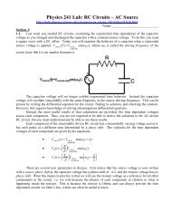
XXXIV International School on the Physics of Semiconducting ...
XXXIV International School on the Physics of Semiconducting ...
XXXIV International School on the Physics of Semiconducting ...

Create successful ePaper yourself
Turn your PDF publications into a flip-book with our unique Google optimized e-Paper software.
Imaging Coherent Electr<strong>on</strong> FlowBrian LeRoyDelft University <strong>of</strong> TechnologyHarvard UniversityJune 10, 2005www.mb.tn.tudelft.nlleroy@mb.tn.tudelft.nl
3.1.2 Transmitir N IN vezes cada um dos símbolos da c<strong>on</strong>stelação.É preciso c<strong>on</strong>hecer a mensagem transmitida no receptor, o quetorna esta fase supervisi<strong>on</strong>ada. Uma vez recebidos os símbolos, éfeita uma média aritmética entre as amostras corresp<strong>on</strong>dentes acada um deles, o que nos dá uma estimativa inicial de cada umdos símbolos da c<strong>on</strong>stelação distorcida. Algumasparticularizações deste passo serão comentadas na seção 4.1.3.1.3 As estimativas obtidas no passo anterior são então usadascomo c<strong>on</strong>dição inicial para a rede neural. Com isto, os neurôniosjá estarão identificados com cada um dos símbolos transmitidos.3.2. Treinamento:Esta fase serve para que seja refinada, se c<strong>on</strong>statada talnecessidade, a estimativa inicial obtida na fase anterior, antes quea rede comece a operar.3.2.1. Separar um c<strong>on</strong>junto de N T vetores y(k) recebidos para otreinamento e ajuste da rede neural.3.2.2. Para cada vetor y(k), obter o índice do neurônio vencedor,através de:i = arg min ( || w j (k) – y(k) || ) (11)j<strong>on</strong>de w j (k) é o vetor do j-ésimo neurônio no instante k.3.2.3. Uma vez obtido o índice i, utilizar a seguinte fórmula deatualização dos pesos do i-ésimo neurônio:w i (k+1) = w i (k) + α[y(k) – w i (k)] (12)<strong>on</strong>de α é o passo de adaptação.3.2.4. Se julgar-se necessário, embaralhar os N T padrões e voltara 3.2.1.3.3. Operação:Após as duas fases anteriores, c<strong>on</strong>sidera-se que a rede está apta aoperar como decisor ótimo (de acordo com o critério ML). Oprocesso de decisão c<strong>on</strong>siste em se determinar, para cada vetorrecebido y(k), o neurônio que tem o vetor de pesos mais próximodesta entrada. Como os neurônios já foram devidamenteidentificados, o símbolo corresp<strong>on</strong>dente ao vencedor é aestimativa de nosso decisor.É muito importante que a rede c<strong>on</strong>tinue a ser adaptada nosmoldes de 3.2.2 e 3.2.3 para todos os símbolos, para compensareventuais modificações do canal. Isto caracteriza a operação “<strong>on</strong>line”do decisor já devidamente treinado.4. APLICAÇÃO A SISTEMAS 4-PSK E 16-QAM COM VARIAÇÕES DE GANHO EFASEDentre as muitas possíveis escolhas para uma base ort<strong>on</strong>ormal,iremos c<strong>on</strong>centrar-nos neste trabalho em apenas uma: uma baseformada por duas senóides de mesma frequência e defasadas denoventa graus (cosseno e seno). Esta escolha permite-nosabranger uma ampla classe de esquemas de modulação digital.Iremos c<strong>on</strong>centrar nossa análise em dois exemplos significativos:modulações 4-PSK e 16-QAM. No primeiro caso, a informaçãoestá embutida na fase da portadora senoidal. No segundo, ainformação enc<strong>on</strong>tra-se na fase e na amplitude da portadora.A comp<strong>on</strong>ente associada ao termo cossenoidal da base échamada de comp<strong>on</strong>ente em fase, e o outro termo denomina-secomp<strong>on</strong>ente em quadratura. O c<strong>on</strong>junto de possíveis vetores decomp<strong>on</strong>entes do alfabeto do transmissor denomina-sec<strong>on</strong>stelação.Na exposição a seguir, foi arbitrado o valor da energia de cadasímbolo, sem perda de generalidade, e este valor foi usado noresto do trabalho.4.1. Esquema para a modulação 4-PSKNa modulação 4-PSK, há 4 possibilidades para as comp<strong>on</strong>entesde x :X 4-PSK = { [-1; -1], [-1; 1], [1; -1], [1; 1] } (13)Analisando esta c<strong>on</strong>stelação, percebe-se que a mesma ésimétrica. Isto permite que exploremos esta característica paraotimizar o algoritmo descrito na seção 3. Mais especificamente, opasso 3.1.2 pode ser alterado. Ao invés de enviarmos os quatrosímbolos desta c<strong>on</strong>stelação, basta que enviemos um deles (N INvezes). Feita a média, temos a c<strong>on</strong>dição inicial de um dosneurônios. Para obtermos a dos outros, basta imprimir 3deslocamentos de 90 o sucessivos, sendo que o vetor resultante decada deslocamento é c<strong>on</strong>siderado como c<strong>on</strong>dição inicial de umdos 3 neurônios restantes. A isto denominamos inicializaçãoortog<strong>on</strong>al da rede, que então estará pr<strong>on</strong>ta para a fase 3.2.4.2. Esquema para a modulação 16-QAMNa modulação 16-QAM, há dezesseis possíveis símbolos:X 16-QAM = {[-3; -3], [-3; -1], [-3; 1], [-3; 3], [-1; -3],[-1; -1], [-1; 1], [-1; 3], [1; -3], [1; -1], [1; 1], [1; 3], (14)[3; -3], [3; -1], [3; 1], [3; 3]}Os quadrantes do plano no qual se enc<strong>on</strong>tra a c<strong>on</strong>stelaçãoexpressa em (14) serão denominados por nós quadrantesmaiores. Dentro de cada um destes, podemos definir outrosquadrantes, de modo a ser ter cada um dos quatro símbolos dac<strong>on</strong>stelação, simetricamente distribuídos, em um dos chamadosquadrantes menores. Portanto, cada símbolo pode sercaracterizado pela indicação dos seus quadrantes maior e menor.A princípio, pode-se propor um decisor baseado em 16 neurônios(um por símbolo), de forma análoga ao caso anterior. Podemos,porém, explorar as características de simetria da c<strong>on</strong>stelação 16-QAM para reduzir este número.Neste artigo, propomos um esquema baseado em quatr<strong>on</strong>eurônios para obter uma aproximação do decisor ótimo.Novamente, utilizamos a idéia de inicialização ortog<strong>on</strong>al,descrita na seção 4.1, sendo transmitido apenas o símbolo demaior potência de um dos quadrantes. Isto permite a realizaçãodo passo 3.1.2 na melhor SNR possível, tornando o algoritmomais robusto ao efeito do ruído.
Two-dimensi<strong>on</strong>al electr<strong>on</strong> gasQuantum Point C<strong>on</strong>tact GateOhmic C<strong>on</strong>tactGaAs/AlGaAs HeterostructureTwo-Dimensi<strong>on</strong>al Electr<strong>on</strong> Gas (2DEG)2DEG located 57 nm below surface
EF2DEG propertiesFree electr<strong>on</strong>s in 2D with a reduced mass2 2kF1= = m v*2m2 ** 2F= 0.067meLow (tunable) electr<strong>on</strong> density and l<strong>on</strong>g Fermi wavelength2π2π11 2λ = = 39nm n = = 4.2×10 / cmFk FHigh mobility and l<strong>on</strong>g elastic mean free pathµ = 1.0 x 10 6 cm 2 */V s = vmµ e=11µmλF2FmGood review article for basics about 2DEG and quantum point c<strong>on</strong>tactsBeenakker and van Houten, Solid State <strong>Physics</strong> 44 1 (1991) (c<strong>on</strong>d-mat/0412664)
Quantum point c<strong>on</strong>tactsElectr<strong>on</strong>s flowing through a narrow c<strong>on</strong>stricti<strong>on</strong>Ohmic c<strong>on</strong>tactElectrostatic gate300nmClassicalQuantumWidth
EF+ δµJn = e ∫ ρn( E)vndEEFCurrent in 1-DCalculate <strong>the</strong> current carried by a single modeJvelocityDensity <strong>of</strong> statesnρ ( ) nE2e 2e= δµ = ∂Vπ hdN 1 1= =dE π vDensity <strong>of</strong> states and velocity cancelIn 1-D each mode carries <strong>the</strong> same amount <strong>of</strong> currentF
Quantum point c<strong>on</strong>tacts-quantizati<strong>on</strong>What is <strong>the</strong> differential c<strong>on</strong>ductance?∞0∂IG ≡ =∂V2ehWhat are <strong>the</strong> values <strong>of</strong> Tn?T⎧0= ⎨⎩12∑n FnEn< EFAssume 1-D particle-in-a-box <strong>of</strong> width LEn= E whenFFinite temperature blurs <strong>the</strong> c<strong>on</strong>ductance plateaus2 ∞df 2eGET ( , ) = ∫ GE ( ,0) dE= ∑ f( En−EF)dE hFEL =i>TnλF2iEn=1
Quantum point c<strong>on</strong>tacts-modesC<strong>on</strong>ductance vs. Gate Voltage14121086420-1.2 -1.0 -0.8 -0.6Gate Voltage (Volts)T = 1.7 KTunneling Regime 1st Mode 2nd Mode
Quantum point c<strong>on</strong>tact-energy levelsC<strong>on</strong>ductanceGate Voltage6 66554 4 4332 2 2g = 2e 2 /hg = e 2 /h101g = 2e 2 /hV sd
Quantum point c<strong>on</strong>tact-energy levelsPlot <strong>of</strong> dG/dV gRed areas are plateaus,yellow and blue are steep14121086420-1.2 -1.0 -0.8 -0.6Gate Voltage (Volts)Horiz<strong>on</strong>tal distance between edges <strong>of</strong>diam<strong>on</strong>ds gives subband spacing
Outline• Introducti<strong>on</strong>• Measurement technique• Imaging a quantum point c<strong>on</strong>tact• Interference fringes• Measuring electr<strong>on</strong> density• Electr<strong>on</strong> optics• Electr<strong>on</strong>-electr<strong>on</strong> interacti<strong>on</strong>s• C<strong>on</strong>clusi<strong>on</strong>s
Liquid helium temperature scanningprobe microscope - cantileverAFM CantileverTip∆R cR c= 4 x 10 -7 /ÅR c ≈ 2000 ΩV BiasRR C25µmRRVV out∆R∝V outµ ∆R outcRVcV biasBias
Liquid helium temperature scanning probemicroscope – scan tubeWheatst<strong>on</strong>eBridgeFeedbackCircuitCross Secti<strong>on</strong>+V y1”-V x V z-V y+V xPiezoelectric TubeScan Range 20µm
Liquid helium temperature scanning probemicroscopeHeight50 nm1µm0 nm
Experimental techniqueAFM CantileverQuantum PointC<strong>on</strong>tact (QPC) GateTwo-dimensi<strong>on</strong>alElectr<strong>on</strong> Gas (2DEG)GaAs/AlGaAsheterostructuren-type GaAssubstratePerturbati<strong>on</strong> from tip causes scatteringwhich changes <strong>the</strong> c<strong>on</strong>ductance <strong>of</strong> <strong>the</strong> QPCImage obtained by measuring c<strong>on</strong>ductancethrough <strong>the</strong> QPC as a functi<strong>on</strong> <strong>of</strong> tip positi<strong>on</strong>High flow High scattering High signalNo flow No scattering No signal
Weak ScattererImaging mechanismNo Backscattering=C<strong>on</strong>ductance UnchangedStr<strong>on</strong>g ScattererBackscattering=C<strong>on</strong>ductance Reduced
Effect <strong>of</strong> tip height10 nm 15 nm 20 nm 25 nm 30 nm 35 nm150nm 150nm 150nm 150nm 150nm 150nm0.140.120.100.080.060.040.020.000204060Height (nm)∆G: 0 e 2 /h 1.6 e 2 /h80100Tip voltage -3.5 VoltsSignal <strong>on</strong>ly when voltage <strong>on</strong>tip depletes <strong>the</strong> 2DEG
Electrostatic simulati<strong>on</strong>n ⎛sV ⎞ εε0∆ n( ρ ) = V2 ⎜ ⎟+1 + / ⎝Vd⎠ d + εh( ρ d )Induced chargen
Quantum mechanical simulati<strong>on</strong>GatesTip0.040.030.020.010.0020406080100Height (nm)Signal <strong>on</strong>ly when tip depletes 2DEG
Importance <strong>of</strong> depleti<strong>on</strong> regi<strong>on</strong>V tip-3.0V V tip-2.6V V tip-2.2V V tip-1.8V V tip0.0V V tip+3.0V50 nm0.060.040.02-3 -2 -1 0 1 2 3Tip Voltage (V)
Imaging requirementsPerturbati<strong>on</strong> from tip must backscatterelectr<strong>on</strong>s through <strong>the</strong> QPC.This requires that <strong>the</strong>re is an area depleted <strong>of</strong>electr<strong>on</strong>s beneath <strong>the</strong> tip.Can be accomplished by ei<strong>the</strong>r bringing tip closeto surface or increasing <strong>the</strong> tip voltageImaging <strong>on</strong>ly works with a negative tip voltageSize <strong>of</strong> perturbati<strong>on</strong> is set by distancebetween <strong>the</strong> tip and <strong>the</strong> 2DEGApproximately Lorentzian in shape
Outline• Introducti<strong>on</strong>• Measurement technique• Imaging a quantum point c<strong>on</strong>tact• Measuring electr<strong>on</strong> density• Interference fringes• Electr<strong>on</strong> optics• Electr<strong>on</strong>-electr<strong>on</strong> interacti<strong>on</strong>s• C<strong>on</strong>clusi<strong>on</strong>s
Topinka, LeRoy et al., Science 289, 2323 (2000)Imaging a quantum point c<strong>on</strong>tact1st Plateau 2nd Plateau 3rd Plateau∆G:0 e 2 /h -1.7e 2 /h
Coherent fringesC<strong>on</strong>structive & Destructive BackscatteringFringes spaced by λ F /2C<strong>on</strong>structive Interference: 2k F L = 2π nDestructive Interference: 2k F L = 2π (n+1/2)
Opening QPCNew Modes <strong>of</strong> current <strong>on</strong>ly appear <strong>on</strong> plateausPattern remains c<strong>on</strong>stant between plateaus
Heating electr<strong>on</strong>sSmall Bias Voltage V bias = 0.2mVG = 2e 2 /h G = 4e 2 /h G = 6e 2 /hLarge Bias Voltage V bias = 3.0 mVG = 2e 2 /hG = 4e 2 /hG = 6e 2 /h∆G: 0 e 2 /h 1.7 e 2 /hLarge bias voltage heats electr<strong>on</strong>sBlurred interference fringes
Extracting a modal patternExperiment TheoryExperimentTheoryDerivati<strong>on</strong>2nd Mode Flow 2nd Plateau Flow 1st Plateau Flow
Modal summaryExperimentTheory1st Mode2nd Mode3rd Mode∆G(percent)|Ψ | 2(arb unit)
Selective mode suppressi<strong>on</strong>No TipTip Blocking CenterTipTip Blocking SideTip500 nm500 nm500 nm64201.7e 2 /h2.0e 2 /hV g (Volts)Tip selectively modifies transmissi<strong>on</strong> coefficient <strong>of</strong> individual modes
Electr<strong>on</strong>-wave flow through 2DEG“Idealized” 2DEG Potential& Electr<strong>on</strong> WaveActual 2DEG Potential &Electr<strong>on</strong> Wave?2µmOperating Point2µmOperating Point
Coherent electr<strong>on</strong> flow through a 2DEG1µm∆G: 0 e 2 /h 0.4 e 2 /h
Modal patterns far away from QPC1st Mode2nd Mode3rd Mode4th Mode∆G: 0 e 2 /h 0.4 e 2 /h
Simulated imageDoes <strong>the</strong> presence <strong>of</strong> <strong>the</strong> tip influence <strong>the</strong> image?Simulated electr<strong>on</strong> flowSimulated imageImage <strong>the</strong> unperturbed electr<strong>on</strong> flow
Unexpectedly high resoluti<strong>on</strong>100nmTip Perturbati<strong>on</strong> ~ 120nm FWHMbutFringe Resoluti<strong>on</strong> ~ better than 10nmLateral Resoluti<strong>on</strong> ~ better than 20nm
Unperturbed Currentand Tip Perturbati<strong>on</strong>High spatial resoluti<strong>on</strong>Tip Moving Through Current
Quantum and classical simulati<strong>on</strong>s0.2 E FPotential, U(x,y)1µm-0.2 E FClassical1µmQuantum Mechanical1µmTopinka, LeRoy et al., Nature 410, 183 (2001)
Formati<strong>on</strong> <strong>of</strong> CausticsClassical TrajectoriesPy-y Phase SpacePotential Dip
QPC Locati<strong>on</strong> shifts by 20 nmMoving QPC locati<strong>on</strong>500 nm
Shifting QPCUnequal voltage <strong>on</strong> QPC gates∆Ge 2 /h0.01500 nm230.4Difference <strong>of</strong> <strong>the</strong> two scans1G diff-0.1e 2 /h500 nm500 nm0.0e 2 /h0.1e 2 /h
Mapping 2DEG potentialTip Locati<strong>on</strong>s0.5Potential?∆G (e 2 /h)0.40.30.2200 nm0.1-4.0 -3.5 -3.0 -2.5 -2.0Tip Voltage (Volts)
Imaging a QPCImaged electr<strong>on</strong> flow near a quantum point c<strong>on</strong>tactModal pattern associated withwavefuncti<strong>on</strong>s in QPCInterference fringes spaced by λ F /2Imaged electr<strong>on</strong> flow far from a quantum point c<strong>on</strong>tactElectr<strong>on</strong> flow forms narrow branchesBranches are due to caustics caused by dipsin <strong>the</strong> potentialInterference fringes spaced by λ F /2
Outline• Introducti<strong>on</strong>• Measurement technique• Imaging a quantum point c<strong>on</strong>tact• Interference fringes• Measuring electr<strong>on</strong> density• Electr<strong>on</strong> optics• Electr<strong>on</strong>-electr<strong>on</strong> interacti<strong>on</strong>s• C<strong>on</strong>clusi<strong>on</strong>s
Interference fringesPresence <strong>of</strong> interference fringes showsthat electr<strong>on</strong>s are coherentUse interference to create new types <strong>of</strong> devicesthat rely not <strong>on</strong>ly <strong>on</strong> amplitude <strong>of</strong> signal but also<strong>the</strong> phase informati<strong>on</strong>Want to understand what causes<strong>the</strong> interference fringesCan this interference also be c<strong>on</strong>trolled?
Coherent fringesC<strong>on</strong>structive & Destructive BackscatteringFringes spaced by λ F /2C<strong>on</strong>structive Interference: 2k F L = 2π nDestructive Interference: 2k F L = 2π (n+1/2)
Finite temperature- <strong>the</strong>rmal smearingFermi energy for free electr<strong>on</strong>s in a 2DEG2 2kF1 * 2EF= = m v*F m* = 0.067me2m2Electr<strong>on</strong>s are not m<strong>on</strong>oenergetic, <strong>the</strong>y have a range <strong>of</strong>energy from <strong>the</strong> finite temperatureC<strong>on</strong>sider two electr<strong>on</strong>s that differ in energy by 2kTThey will have slightly different wavevectors, k2 2k,E = ,E ± FkT = + −+− *2mAssume kT
Thermal smearing (c<strong>on</strong>tinued)Now suppose <strong>the</strong>se electr<strong>on</strong>s interfere after a distance LEach <strong>of</strong> <strong>the</strong> electr<strong>on</strong>s will have accumulated a phase, kLSo, <strong>the</strong>ir phase difference is2kT2∆ kL =v Define <strong>the</strong> <strong>the</strong>rmal length as when this phase difference is 1LtFLvF= L t ~ 200 nm @ 4.2 K2kTThe <strong>the</strong>rmal length can be better defined by using <strong>the</strong> spread in energy <strong>of</strong> <strong>the</strong>Fermi distributi<strong>on</strong>
Thermal smearing (c<strong>on</strong>tinued)As <strong>the</strong> length is increased, <strong>the</strong> range <strong>of</strong> accumulated phaseswill start to wash out <strong>the</strong> interference fringesEach electr<strong>on</strong> accumulates a different phase <strong>on</strong> <strong>the</strong>roundtrip from <strong>the</strong> tip to <strong>the</strong> QPC.Expectati<strong>on</strong>:Fringes decay with distance from QPCNote: The electr<strong>on</strong>s have not lost <strong>the</strong>ir coherence itis <strong>on</strong>ly being “hidden” by <strong>the</strong> <strong>the</strong>rmal smearing
Fringe persistence1D model <strong>of</strong> fringe persistence, calculate transmissi<strong>on</strong>through two delta functi<strong>on</strong>s as a functi<strong>on</strong> <strong>of</strong> positi<strong>on</strong>Fringe amplitude decays with distance
Fringe persistenceFringe Size (%)Distance from QPC (nm)No distance dependence observed
Backscattering from Tip and Impurities...Calculate wave backscattered to <strong>the</strong> QPC2ikRtip2ikR A itipeAeiΨ= +∑Rtipi RiLook at <strong>the</strong> amplitude <strong>of</strong> terms that vary with tip positi<strong>on</strong>2Ψ = 2Re∑AA eitipi i tip2 ik ( R −R)RRFinite temperature Range <strong>of</strong> wavevectorssignaltip2 ∂f = ∫ Ψ dE ∂ Ei
Fringe persistence far from <strong>the</strong> QPCIntegrand oscillates rapidly with energy except for terms with R i ≈ R tipAA2 2i tip−( Rtip −Ri ) / TsR (tip) = 2∑cos⎡2 kF ( Rtip −Ri) ⎤eRR ⎣⎦i i tipT=2k1/2 Fπ/4mkTTipImpurityAnnular band, width = TCombined backscattering <strong>of</strong>f <strong>the</strong> tip and <strong>the</strong> impurities in <strong>the</strong> annularband around r tip produces interference fringes spaced at λ F /2**S.E.J. Shaw et al, c<strong>on</strong>d-mat/0105354 (2001)Test this <strong>the</strong>ory with an artificial scatterer
Fringe persistence far from <strong>the</strong> QPCImpurityTipAnnular band, width = <strong>the</strong>rmal lengthCombined backscattering <strong>of</strong>f <strong>the</strong> tip and <strong>the</strong> impurities in <strong>the</strong> annularband around r tip produces interference fringes spaced at λ F /2**S.E.J. Shaw et al, c<strong>on</strong>d-mat/0105354 (2001)Test this <strong>the</strong>ory with an artificial scatterer
Scattering induced fringe enhancementQPC GatesReflectorImpuritiesScan Area∆G(e 2 /h)0.00.05V refl = 0 VV refl = -0.4 VV refl = -0.8 V
ReflectorVoltageFringe strength analysis0.0 Volts-0.4 Volts-0.8 Volts∆G (e 2 /h)FFT (arb. units)0.00 0.05 0 300Reflector enhances interference fringes
Single BounceFringe movementDouble BounceDouble100 nmSingle100 nmMovies range from V refl = -0.5 V to -1.0V in steps <strong>of</strong> 0.02 VReflecting ArcFringes move twice as fast attwice <strong>the</strong> distance from <strong>the</strong> QPCLeRoy et al., PRL 94 126801 (2005)
Single BounceFringe movementDouble BounceAverage Peak Movement0.10 µm/VoltAverage Peak Movement0.23 µm/VoltInterference fringes at twice <strong>the</strong> radius <strong>of</strong> <strong>the</strong> reflecting arcmove twice <strong>the</strong> speed <strong>of</strong> <strong>the</strong> arc
Fringe amplitudeFringes enhancedReflector backscattering suppressedFringes suppressedReflector backscattering enhancedFringe amplitude anti-correlated with reflector c<strong>on</strong>ductance
Heating electr<strong>on</strong>s1.7KQPC GatesReflector“4.2K”Scan Area“8.4K”
Temperature dependenceIncreased temperature destroys interference away from reflector
Interference fringesSpaced by half <strong>the</strong> Fermi wavelength, λ F /2Due to interference between electr<strong>on</strong>s backscattered by<strong>the</strong> tip an <strong>on</strong>es backscattered from impuritiesPersist throughout image because <strong>of</strong> backscattering fromimpuritiesCan c<strong>on</strong>trol <strong>the</strong>ir locati<strong>on</strong> by introducing artificial impuritiesDem<strong>on</strong>strated <strong>the</strong>ir movementwith a reflecting gateThey become more localized withincreasing temperature
Outline• Introducti<strong>on</strong>• Measurement technique• Imaging a quantum point c<strong>on</strong>tact• Interference fringes• Measuring electr<strong>on</strong> density• Electr<strong>on</strong> optics• Electr<strong>on</strong>-electr<strong>on</strong> interacti<strong>on</strong>s• C<strong>on</strong>clusi<strong>on</strong>s
Therefore want a local probe <strong>of</strong> densityMeasuring densityElectr<strong>on</strong> density measured by Shubnikov-de Haas oscillati<strong>on</strong>sgives <strong>the</strong> average value over <strong>the</strong> entire sample.Usually a Hall bar <strong>of</strong>~ 100 micr<strong>on</strong>sns=2e1h ∆( 1 B)For nanoscale devices, important to be able to measure <strong>the</strong>density in <strong>the</strong> vicinity <strong>of</strong> <strong>the</strong> device
Electr<strong>on</strong> densityFree electr<strong>on</strong>s in two dimensi<strong>on</strong>s2 2kEF= **m2m=0.067meFermi surface is a circle2 2⎛ k ⎞ kn = 2π⎜ ⎟ =⎝2π⎠ 2πWavelength <strong>of</strong> interference pattern is related to kUse interference <strong>of</strong> electr<strong>on</strong> waves
Changing Fermi energyEffect <strong>of</strong> reducing Fermi Energy from 15 meV to 5 meV500 nmReducing Fermi Energy increases relative strength <strong>of</strong>bumps and dips in potential
Effect <strong>of</strong> reducing Fermi energyBack Gate 0 V Back Gate -1 V Back Gate -3 V Back Gate -5 V∆G: 0 e 2 /h 0.15 e 2 /hReducing Fermi energy, increases fringe spacing andcauses flow to be more diffuse
Measuring local electr<strong>on</strong> densityDensity Decreases, Wavelength IncreasesBack gate -1V Back gate -3V Back gate -5V2DEGWafer Pr<strong>of</strong>ileMeasured Density1.12 µm GaAs0.82 µm Al 0.3 Ga 0.7 Asn-type GaAsBackgateParallel platecapacitor model∆ n =11 -20.36 × 10 cm V∆VLeRoy et al., APL 80 4431 (2002)
Is it really local?Calculate spacing between two adjacent fringesPhase accumulated, φNeed phase to change by 2π, must move tip by LL=πkk is wavevector at this locati<strong>on</strong>Yes it is local, with resoluti<strong>on</strong> ~ fringe spacing
Mapping electr<strong>on</strong> density∆G(e 2 /h)0.00200 nm0.15Average Density, n = 2.95 x 10 11 cm -2Standard Deviati<strong>on</strong> σ = 0.48 x 10 11 cm -2
Electr<strong>on</strong> densityInterference fringes provide a way to measure<strong>the</strong> local electr<strong>on</strong> densityspacing =π2nDensity can be c<strong>on</strong>trolled by back gate voltagePattern <strong>of</strong> flow become more diffuse asdensity is decreasedPotential felt by <strong>the</strong> electr<strong>on</strong>s becomes a largefracti<strong>on</strong> <strong>of</strong> <strong>the</strong>ir energy at low density
Outline• Introducti<strong>on</strong>• Measurement technique• Imaging a quantum point c<strong>on</strong>tact• Interference fringes• Measuring electr<strong>on</strong> density• Electr<strong>on</strong> optics• Electr<strong>on</strong>-electr<strong>on</strong> interacti<strong>on</strong>s• C<strong>on</strong>clusi<strong>on</strong>s
Electr<strong>on</strong> opticsCreate elements to electrostatically c<strong>on</strong>trol electr<strong>on</strong>sElectrostatic lensSivan et al., PRB 41 7937 (1990)Image how electr<strong>on</strong>s travel through <strong>the</strong>se types <strong>of</strong> devices
Electr<strong>on</strong> optics <strong>the</strong>oryAnalog to Optical Index <strong>of</strong> Refracti<strong>on</strong>…p Sin( θ ) = p Sin( θ )1 1 2 2n Sin( θ ) = n Sin( θ )1 1 2 2
Electr<strong>on</strong> optics element - prism1µm“Refractive switch for two-dimensi<strong>on</strong>al electr<strong>on</strong>s”, J. Spector, H. L. Stormer, K. W.Baldwin, L. N. Pfeiffer, and K. W. West , App Phys Let 56, 2433-2435 (1990)
Electr<strong>on</strong> optics element - ballBall 0.0 VBall -0.5 V∆Ge 2 /h0.00.5Additi<strong>on</strong> <strong>of</strong> <strong>the</strong> ball creates elliptical interference fringes
Electr<strong>on</strong> optics element - channel∆Ge 2 /h0.00.75Simulated TrajectoryElectr<strong>on</strong> trajectories are bent by <strong>the</strong> potential from <strong>the</strong> gate
Electr<strong>on</strong> opticsImaged electr<strong>on</strong>s traveling through <strong>the</strong> following devicesElectrostatic prismReflecting ballChannelCan learn about <strong>the</strong> potential from electrostatic gatesThe images show why it is difficult to make efficientdevices with <strong>the</strong>se type <strong>of</strong> gatesBranches <strong>of</strong> current limit <strong>the</strong> abilityto c<strong>on</strong>trol <strong>the</strong> flow
Outline• Introducti<strong>on</strong>• Measurement technique• Imaging a quantum point c<strong>on</strong>tact• Interference fringes• Measuring electr<strong>on</strong> density• Electr<strong>on</strong> optics• Electr<strong>on</strong>-electr<strong>on</strong> interacti<strong>on</strong>s• C<strong>on</strong>clusi<strong>on</strong>s
Interacti<strong>on</strong>sTo design devices relying <strong>on</strong> quantum informati<strong>on</strong> musthave a way to measure time (distance) over which <strong>the</strong>electr<strong>on</strong>s decohere.At low temperatures, electr<strong>on</strong>-electr<strong>on</strong> interacti<strong>on</strong>s limit<strong>the</strong> distance electr<strong>on</strong>s remain coherent in <strong>the</strong> 2DEGIn order to create devices relying <strong>on</strong> coherencemust be able to measure <strong>the</strong> electr<strong>on</strong>-electr<strong>on</strong>scattering time12∼ ( p−pF) ln ( p−pF)τeeImages can give a direct measure <strong>of</strong> this scattering time
DC bias techniqueNo Energy LossC<strong>on</strong>ductance ReducedEnergy LossC<strong>on</strong>ductance Unchanged
Voltage applied across QPC0.0 meV Across QPC∆ge 2 /h0.02.4 meV Across QPC0.4
Images <strong>of</strong> electr<strong>on</strong> flow2.74 µm from QPC 1.96 µm from QPC 1.20 µm from QPC∆G (e 2 /h)0.00 0.1350 nm 50 nm50 nm0.00 0.35 0.00 0.55E FE FTipQPCMovies range from 0.0 mV to 3.1 mV in steps <strong>of</strong> 0.15 mV
Measuring electr<strong>on</strong> energyFringe spacing indicates energy <strong>of</strong> electr<strong>on</strong>s
Measuring e-e scattering lengthElectr<strong>on</strong>-Electr<strong>on</strong> Scattering Time21 E ⎛F∆ ⎞ ⎡ ⎛EF ⎞ ⎛2q⎞TF1⎤= ⎜ ⎟ ⎢ln⎜ ⎟+ ln ⎜ ⎟+⎥τee 4π⎝EF ⎠ ⎣ ⎝ ∆ ⎠ ⎝ pF⎠ 2⎦Valid at T=0, ∆ is excess energyGiuliani and Quinn, PRB 26, 4421 (1982).What is probability that an electr<strong>on</strong> can travel distance L without a collisi<strong>on</strong>?2⎡ ⎤ ⎡ ⎤LL⎛∆ ⎞P~ Exp⎢− ⎥ ~ Exp⎢− ⎜ ⎟ ⎥⎢ vτv EF⎣ ee⎥⎦⎢⎣⎝ ⎠ ⎥⎦Signal relies <strong>on</strong> electr<strong>on</strong>s not colliding should decay like a gaussian…E FAssuming τ ee< τ elE FTipQPC
Differential c<strong>on</strong>ductance vs. excess energySignal decays more quickly at l<strong>on</strong>ger distances from <strong>the</strong> QPC0.6 µm0 meV 1 meV 2 meV 3 meV∆g(e 2 /h)0.001.4 µm50 nm0.55∆g(e 2 /h)0.0050 nm0.13
Differential c<strong>on</strong>ductance vs. excess energySignal decays more quickly with increasing back gate voltage0 meV 1 meV 2 meV 3 meVBack Gate 0V∆g(e 2 /h)0.0050 nmBack Gate -2V0.3550 nm
Signal Vs. excess energySignal decays more quickly at l<strong>on</strong>ger distances from <strong>the</strong> QPCSignal decays more quickly with increasing back gate voltage
Interacti<strong>on</strong>sImages are sensitive to whe<strong>the</strong>r or not an electr<strong>on</strong> haslost energyThis is used to measure <strong>the</strong> distance over whichelectr<strong>on</strong>s remain coherentThe measurements show that <strong>the</strong> scattering time depends<strong>on</strong> <strong>the</strong> Fermi energy and <strong>the</strong> excess applied energy.21 E ⎛F∆ ⎞ ⎡ ⎛EF ⎞ ⎛2q⎞TF1⎤= ⎜ ⎟ ⎢ln⎜ ⎟+ ln ⎜ ⎟+⎥τee 4π⎝EF ⎠ ⎣ ⎝ ∆ ⎠ ⎝ pF⎠ 2⎦
ExperimentAcknowledgementsHarvard UniversityTheoryMark TopinkaAnia BleszynskiKathy AidalaRobert WesterveltScot ShawAllis<strong>on</strong> KalbenEric HellerUniversity <strong>of</strong> California – Santa BarbaraKevin MaranowskiArt Gossard
Image pattern <strong>of</strong> electr<strong>on</strong>flow from a QPCC<strong>on</strong>clusi<strong>on</strong>sC<strong>on</strong>trol interference fringesImage local electr<strong>on</strong> densityImage electr<strong>on</strong> flow throughelectr<strong>on</strong> optics elementsImage electr<strong>on</strong>-electr<strong>on</strong> scattering
Current workCombined scanning tunneling spectroscopy andtransport measurements <strong>of</strong> carb<strong>on</strong> nanotubesPh<strong>on</strong><strong>on</strong> generati<strong>on</strong> and absorpti<strong>on</strong>LeRoy et al., Nature 432 374 (2004)
Improved fringe resoluti<strong>on</strong>Wiggling Tip VoltageFixed Tip Voltage100nm100nmdI/dVtip (nA/V)1.1 -0.80.0∆G (e 2 /h)0.6Wiggling tip voltage, images <strong>the</strong> spatial derivative <strong>of</strong> <strong>the</strong> flow
Imaging with AC voltage <strong>on</strong> tipTip Voltage SeriesBias Voltage Series100 nmTip Voltage goes from 0 to -3.5 V100 nmBias Voltage goes from -6.25 to 6.25 mV