2007 Issue 2 - Raytheon
2007 Issue 2 - Raytheon
2007 Issue 2 - Raytheon

You also want an ePaper? Increase the reach of your titles
YUMPU automatically turns print PDFs into web optimized ePapers that Google loves.
R F S Y S T E M S<br />
Continued from page 27<br />
completed, affirming <strong>Raytheon</strong>’s leadership<br />
position in the development of this technology.<br />
This testing was done at elevated temperatures<br />
and operating conditions to simulate<br />
performance over a much longer period<br />
of time. Three temperature DC Arrhenius<br />
tests of <strong>Raytheon</strong>’s 28V GaN have also been<br />
completed, and the results predict a mean<br />
time to failure (MTTF) of greater than 1 million<br />
hours at a standard transistor channel<br />
temperature of 150 Celsius. These test<br />
results have given <strong>Raytheon</strong> customers confidence<br />
in the use of <strong>Raytheon</strong>’s GaN for<br />
future defense systems.<br />
To support these efforts, RRFC is presently<br />
transitioning the fabrication of GaN MMICs<br />
into its high-volume 100 mm diameter wafer<br />
production fabrication facility (see Figure 2).<br />
This transition will make GaN available with<br />
the quality (RF performance, reliability and<br />
yield), quantity and affordability necessary<br />
to support systems requirements.<br />
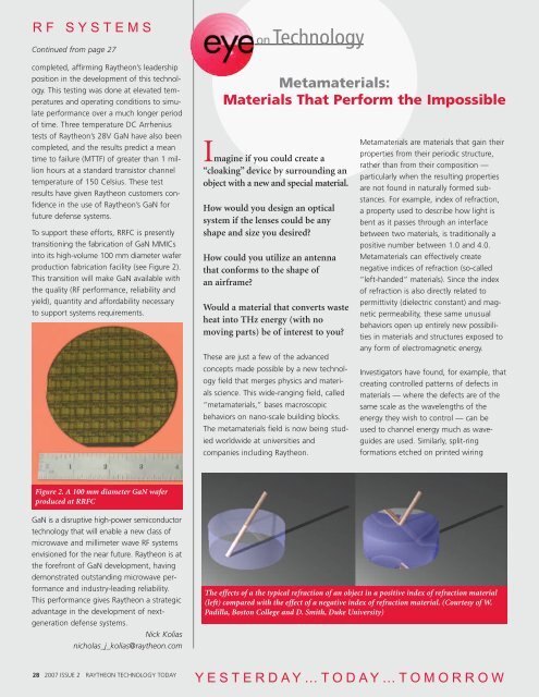
Figure 2. A 100 mm diameter GaN wafer<br />
produced at RRFC<br />
GaN is a disruptive high-power semiconductor<br />
technology that will enable a new class of<br />
microwave and millimeter wave RF systems<br />
envisioned for the near future. <strong>Raytheon</strong> is at<br />
the forefront of GaN development, having<br />
demonstrated outstanding microwave performance<br />
and industry-leading reliability.<br />
This performance gives <strong>Raytheon</strong> a strategic<br />
advantage in the development of nextgeneration<br />
defense systems.<br />
Nick Kolias<br />
nicholas_j_kolias@raytheon.com<br />
28 <strong>2007</strong> ISSUE 2 RAYTHEON TECHNOLOGY TODAY<br />
onTechnology<br />
Metamaterials:<br />
Materials That Perform the Impossible<br />
Imagine if you could create a<br />
“cloaking” device by surrounding an<br />
object with a new and special material.<br />
How would you design an optical<br />
system if the lenses could be any<br />
shape and size you desired?<br />
How could you utilize an antenna<br />
that conforms to the shape of<br />
an airframe?<br />
Would a material that converts waste<br />
heat into THz energy (with no<br />
moving parts) be of interest to you?<br />
These are just a few of the advanced<br />
concepts made possible by a new technology<br />
field that merges physics and materials<br />
science. This wide-ranging field, called<br />
“metamaterials,” bases macroscopic<br />
behaviors on nano-scale building blocks.<br />
The metamaterials field is now being studied<br />
worldwide at universities and<br />
companies including <strong>Raytheon</strong>.<br />
Metamaterials are materials that gain their<br />
properties from their periodic structure,<br />
rather than from their composition —<br />
particularly when the resulting properties<br />
are not found in naturally formed substances.<br />
For example, index of refraction,<br />
a property used to describe how light is<br />
bent as it passes through an interface<br />
between two materials, is traditionally a<br />
positive number between 1.0 and 4.0.<br />
Metamaterials can effectively create<br />
negative indices of refraction (so-called<br />
“left-handed” materials). Since the index<br />
of refraction is also directly related to<br />
permittivity (dielectric constant) and magnetic<br />
permeability, these same unusual<br />
behaviors open up entirely new possibilities<br />
in materials and structures exposed to<br />
any form of electromagnetic energy.<br />
Investigators have found, for example, that<br />
creating controlled patterns of defects in<br />
materials — where the defects are of the<br />
same scale as the wavelengths of the<br />
energy they wish to control — can be<br />
used to channel energy much as waveguides<br />
are used. Similarly, split-ring<br />
formations etched on printed wiring<br />
The effects of a the typical refraction of an object in a positive index of refraction material<br />
(left) compared with the effect of a negative index of refraction material. (Courtesy of W.<br />
Padilla, Boston College and D. Smith, Duke University)<br />
Y E S T E R D A Y … T O D A Y … T O M O R R O W