Low loss depressed cladding waveguide - Aston University ...
Low loss depressed cladding waveguide - Aston University ...
Low loss depressed cladding waveguide - Aston University ...

You also want an ePaper? Increase the reach of your titles
YUMPU automatically turns print PDFs into web optimized ePapers that Google loves.
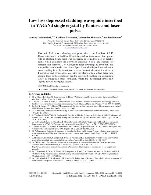
<strong>Low</strong> <strong>loss</strong> <strong>depressed</strong> <strong>cladding</strong> <strong>waveguide</strong> inscribedin YAG:Nd single crystal by femtosecond laserpulsesAndrey Okhrimchuk, 1,2,* Vladimir Mezentsev, 1 Alexander Shestakov, 3 and Ian Bennion 11 Photonics Research Group, <strong>Aston</strong> <strong>University</strong>, Birmingham B4 7ET, UK2 Fiber Optics Research Center of RAS, 38 Vavilova Street, Moscow 119333, Russia3 E.L.S. Co., 3 Vvedensky Street, Moscow 117342, Russia* a.okhrimchuk@aston.ac.ukAbstract: A <strong>depressed</strong> <strong>cladding</strong> <strong>waveguide</strong> with record low <strong>loss</strong> of 0.12dB/cm is inscribed in YAG:Nd(0.3at.%) crystal by femtosecond laser pulseswith an elliptical beam waist. The <strong>waveguide</strong> is formed by a set of paralleltracks which constitute the <strong>depressed</strong> <strong>cladding</strong>. It is a key element forcompact and efficient CW <strong>waveguide</strong> laser operating at 1064 nm andpumped by a multimode laser diode. Special attention is paid to mechanicalstress resulting from the inscription process. Numerical calculation of modedistribution and propagation <strong>loss</strong> with the elasto-optical effect taken intoaccount leads to the conclusion that the <strong>depressed</strong> <strong>cladding</strong> is a dominatingfactor in <strong>waveguide</strong> mode formation, while the mechanical stress onlyslightly distorts <strong>waveguide</strong> modes.©2012 Optical Society of AmericaOCIS codes: (140.3530) Lasers, neodymium; (220.4000) Microstructure fabrication.References and links1. K. M. Davis, K. Miura, N. Sugimoto, and K. Hirao, “Writing <strong>waveguide</strong>s in glass with a femtosecond laser,”Opt. Lett. 21(21), 1729–1731 (1996).2. T. Gorelik, M. Will, S. Nolte, A. Tuennermann, and U. Glatzel, “Transmission electron microscopy studies offemtosecond laser induced modifications in quartz,” Appl. Phys., A Mater. Sci. Process. 76(3), 309–311 (2003).3. L. Gui, B. Xu, and T. C. Chong, “Microstructure in lithium niobate by use of focused femtosecond laser pulses,”IEEE Photon. Technol. Lett. 16(5), 1337–1339 (2004).4. A. V. Streltsov, “Femtosecond-laser writing of tracks with <strong>depressed</strong> refractive index in crystals,” Proc. SPIE4941, 51–57 (2003).5. S. Taccheo, G. Della Valle, R. Osellame, G. Cerullo, N. Chiodo, P. Laporta, O. Svelto, A. Killi, U. Morgner, M.Lederer, and D. Kopf, “Er:Yb-doped <strong>waveguide</strong> laser fabricated by femtosecond laser pulses,” Opt. Lett. 29(22),2626–2628 (2004).6. A. G. Okhrimchuk, A. V. Shestakov, I. Khrushchev, and J. Mitchell, “Depressed <strong>cladding</strong>, buried <strong>waveguide</strong>laser formed in a YAG:Nd 3+ crystal by femtosecond laser writing,” Opt. Lett. 30(17), 2248–2250 (2005).7. J. Siebenmorgen, T. Calmano, K. Petermann, and G. Huber, “Highly efficient Yb:YAG channel <strong>waveguide</strong> laserwritten with a femtosecond-laser,” Opt. Express 18(15), 16035–16041 (2010).8. G. A. Torchia, A. Rodenas, A. Benayas, E. Cantelar, L. Roso, and D. Jaque, “Highly efficient laser action infemtosecond-written Nd:yttrium aluminium garnet ceramic <strong>waveguide</strong>s,” Appl. Phys. Lett. 92(11), 111103(2008).9. J. Thomas, M. Heinrich, J. Burghoff, S. Nolte, A. Ancona, and A. Tünnermann, “Femtosecond laser-writtenquasi-phase-matched <strong>waveguide</strong>s in lithium niobate,” Appl. Phys. Lett. 91(15), 151108 (2007).10. A. Okhrimchuk, “Femtosecond fabrication of <strong>waveguide</strong>s in ion-doped laser crystals,” in Coherence andUltrashort Pulse Laser Emission, F. J. Duarte, ed., (InTech, 2010), pp. 519–542.http://www.intechopen.com/articles/show/title/femtosecond-fabrication-of-<strong>waveguide</strong>s-in-ion-doped-lasercrystals.11. D. G. Lancaster, S. Gross, H. Ebendorff-Heidepriem, K. Kuan, T. M. Monro, M. Ams, A. Fuerbach, and M. J.Withford, “Fifty percent internal slope efficiency femtosecond direct-written Tm³+:ZBLAN <strong>waveguide</strong> laser,”Opt. Lett. 36(9), 1587–1589 (2011).12. A. G. Okhrimchuk, V. K. Mezentsev, H. Schmitz, M. Dubov, and I. Bennion, “Cascaded nonlinear absorption offemtosecond laser pulses in dielectrics,” Laser Phys. 19(7), 1415–1422 (2009).#156893 - $15.00 USD Received 24 Oct 2011; revised 2 Dec 2011; accepted 3 Dec 2011; published 1 Feb 2012(C) 2012 OSA 13 February 2012 / Vol. 20, No. 4 / OPTICS EXPRESS 3832
13. A. G. Okhrimchuk, V. K. Mezentsev, V. V. Dvoyrin, A. S. Kurkov, E. M. Sholokhov, S. K. Turitsyn, A. V.Shestakov, and I. Bennion, “Waveguide-saturable absorber fabricated by femtosecond pulses in YAG:Cr 4+crystal for Q-switched operation of Yb-fiber laser,” Opt. Lett. 34(24), 3881–3883 (2009).14. A. W. Snyder and J. D. Love, Optical Waveguide Theory (Chapman & Hall, 1983).15. R. W. Dixon, “Photoelastic properties of selected materials and their relevance for applications to acoustic lightmodulators and scanners,” J. Appl. Phys. 38(13), 5149–5153 (1967).16. A. Benayas, W. F. Silva, C. Jacinto, E. Cantelar, J. Lamela, F. Jaque, J. R. Vázquez de Aldana, G. A. Torchia, L.Roso, A. A. Kaminskii, and D. Jaque, “Thermally resistant <strong>waveguide</strong>s fabricated in Nd:YAG ceramics bycrossing femtosecond damage filaments,” Opt. Lett. 35(3), 330–332 (2010).IntroductionLaser inscription of <strong>waveguide</strong>s by means of femtosecond (fs) pulses has shown impressiveprogress since its first demonstration in glasses with a femtosecond laser operating at 800 nm[1]. Several years later feasibility of <strong>waveguide</strong> inscription in crystals was also shown [2–4].Femtosecond fabrication of <strong>waveguide</strong> lasers in glasses and crystals has a great practicalimportance since it facilitates manufacturing of extremely compact and reliable laser sources.The first demonstration of a femtosecond written <strong>waveguide</strong> laser was recently reported [5].Eventually, femtosecond written <strong>waveguide</strong> lasers were demonstrated in Nd:YAG [6],Yb:YAG [7] single crystals, and also in Nd:YAG crystalline ceramics [8].In this paper femtosecond written <strong>waveguide</strong>s in crystals are classified as Stress InducedWaveguides (SIW), Depressed Cladding Waveguides (DCW), and directly written<strong>waveguide</strong>s (DRW). The SIW type is formed by a modification of the refractive index due toelasto-optical coupling to mechanical stress induced in the vicinity of a fs inscribed track [2]and between the two tracks [7–9]. Both kinds of such SIWs require a low divergent or evendiffraction limited pump beam in order to confine pump light inside the <strong>waveguide</strong>. The DCWtype comprises of the core, which is the intact domain of a crystal, and a surrounding<strong>depressed</strong> <strong>cladding</strong> composed of parallel tracks with a reduced refractive index [6] wherebythe mechanical stress has minor influence on the <strong>waveguide</strong> modes. A principal feature ofsuch tracks is that there is no detectable manifestation of any irregular damage as opposed tothe SIW type whereby the stress could be accomplished by some damage inside the tracks[2,9]. The DCW type features the lowest propagation <strong>loss</strong> (0.22 dB/cm [6]). Due to geometricflexibility, the <strong>cladding</strong> in DCW may consist of a fairly large number of tracks confining theflexibly large <strong>waveguide</strong> area. This feature is advantageous for coupling to multimode laserdiodes [6,10]. In the DRW type <strong>waveguide</strong>s, a core is formed in the bulk of crystal beingdirectly irradiated by laser pulses. This type was originally observed in [3] and can berelatively easily fabricated in LiNbO 3 crystals.In our previous paper devoted to a CW <strong>waveguide</strong> laser with <strong>depressed</strong> <strong>cladding</strong>fabricated in Nd:YAG single crystal the planar geometry was exploited [6]. In this paper weturn to the multimode <strong>depressed</strong> <strong>cladding</strong> <strong>waveguide</strong> fabricated in YAG:Nd crystal with thecircular core in a pursuit of a better match of multimode fiber used to couple the laser crystalwith a laser diode pump. Such an architecture has also been exploited for theNd:YAG/Cr:YAG Q-switched microchip laser [10], and Tm:ZBLAN CW laser [11]. Sincethe CW regime is more sensitive to the cavity <strong>loss</strong>, we utilized this feature in the present studyfor precise characterization of the propagation <strong>loss</strong>es in DCW with circular cross sectionwritten in Nd:YAG crystal. We also show that DCW inscribed with a beam waist of ellipticalcross section exhibits record low <strong>loss</strong> among all the femtosecond written <strong>waveguide</strong>s incrystals.Fabrication of <strong>waveguide</strong>sThe experimental setup used for <strong>waveguide</strong> inscription is similar to that described in ourprevious experiments [10,12,13]. We used a Ti:Sapphire laser system with pulse duration of110 fs and repetition rate of 1 kHz. The principal distinguishing feature of our experimentalsetup is that in the plane perpendicular to beam propagation the laser beam waist has anelliptical cross section, elongated towards an inscribed track. The beam is focused by a#156893 - $15.00 USD Received 24 Oct 2011; revised 2 Dec 2011; accepted 3 Dec 2011; published 1 Feb 2012(C) 2012 OSA 13 February 2012 / Vol. 20, No. 4 / OPTICS EXPRESS 3833
defocusing cylindrical lens with focal distance f = −34 cm and Mitutoyo lens with NA = 0.55down below the polished surface of YAG:Nd (0.3% at.) at the depth of 70 - 170 µm.Substantial spherical aberration at the air-crystal interface occurs for greater focusing depth. Itleads to elongation of the laser beam in the volume of the sample hence the density of thedeposited energy is reduced. Thus the inscription threshold is remarkably higher for thedepths greater than 200 µm. The crystal was moving at the speed V = 0.5 or 0.7 mm/sperpendicular to the laser beam axis, along the polarization vector. Under these conditions asingle track featuring lower refractive index compared to untreated material was inscribed.Writing of single tracks in YAG: Nd(0.3%at.) has already been investigated under theseconditions [10]. Figure 1 shows the dependence of the Permanent Refractive Index Change(PRICE) and the transverse size of a track parallel to the incident beam (track height) versusinput pulse energy.Fig. 1. Negative permanent refractive index change in Nd(0.3%at.):YAG crystal at thewavelength of 600 nm (squares) and transverse size of a track along inscribing beam (circles)versus energy in femtosecond inscription with 110 fs pulse at wavelength of 800 nm andrepetition rate of 1 kHz. Scan velocity V = 0.5 mm/s. Polarization of femtosecond pulses isparallel to the translation direction. Laser beam is focused at 63 µm below the crystal surface.Four DCWs were fabricated in the same crystal at the depth of 120 µm under the crystalsurface as measured for DCWs centers. The crystal surface was parallel to the (100)crystallographic plane, and the <strong>waveguide</strong>s were parallel to the [010] crystallographic axiswith the accuracy of 5 degrees. The track geometry is shown in Fig. 2. The <strong>waveguide</strong> cladconsists of a chain of tracks forming a tube. The number of tracks in the tube was of 54 or 66(see Table 1) depending on the design. Outer arrays of 3 tracks on the right and left sides wereinscribed to reinforce thin walls of the <strong>cladding</strong> in those positions and to diminish the modeleakage. The <strong>waveguide</strong>s were slightly elliptical with vertical diameter of 116 µm (parallel toincident beam), and horizontal diameter of 110 µm. Waveguide center was at the depth of 120µm under the crystal surface. The main inscription parameters are summarized in Table 1. Weused pulse energies in the range of negligible dependency of PRICE and the track size uponthe pulse energy in order to achieve better reproducibility and uniformity of refractive indexchange (Fig. 1). Thus the magnitude of PRICE in the DCW is typically 0.0025 while the trackheight was of 12 µm.#156893 - $15.00 USD Received 24 Oct 2011; revised 2 Dec 2011; accepted 3 Dec 2011; published 1 Feb 2012(C) 2012 OSA 13 February 2012 / Vol. 20, No. 4 / OPTICS EXPRESS 3834
Fig. 2. Scheme of a <strong>waveguide</strong> consisting of 66 tracks. End view. Waveguide sizes: A = 116µm, B = 110 µm, depth of <strong>waveguide</strong> center h = 120 µm. The red arrow indicates thepropagation direction of inscribing beam.After inscription, the sample was cut in two pieces of 11.4 and 8.1 mm length. Ends of the<strong>waveguide</strong>s were polished, and nearly 200-µm crystal layers containing improperly inscribedtracks ends were removed. Waveguide end facets and the inscribed tracks were madeorthogonal with the accuracy of 10 min. Antireflection dielectric coating for 1064 nm wasapplied to both ends of the 11.4 mm long sample, and the sample of 8.1 mm length wassupplied with the same antireflection dielectric coating on one end, and also with a dichroicmirror on the other end. The dichroic mirror has 100% reflectivity at oscillation wavelength of1064 nm, and transmits 98% at pump wavelength of 809 nm.Pump light waveguidingA fiber coupled laser diode was used for pumping in the oscillation experiments. The fiber hasa core diameter of 105 µm and numerical aperture NA of 0.15. The fiber was winded in twoorthogonal planes to ensure unpolarized pump light. Two alternative schemes for couplingpump diode with a <strong>waveguide</strong> were used. In the first scheme two achromatic lenses with focallength of 3.3 mm each project an image of output end of pumping fiber at the input facet ofone of the 11.4 mm long <strong>waveguide</strong> as seen in Fig. 3(a). Magnification was optimized for thebest match between the core diameters of fiber and the DCW in crystal. A dichroic HR mirrorwas attached to the pumping end. The second scheme utilizes a simple butt-coupling into<strong>waveguide</strong>s in 8.1 mm long sample as shown in Fig. 3(b).Fig. 3. Pump light propagation <strong>loss</strong> measurements. (a) Pump light is coupled through lenses.(b) Butt-coupling.#156893 - $15.00 USD Received 24 Oct 2011; revised 2 Dec 2011; accepted 3 Dec 2011; published 1 Feb 2012(C) 2012 OSA 13 February 2012 / Vol. 20, No. 4 / OPTICS EXPRESS 3835
We made measurements in order to estimate and compare pumping efficiencies of all theinscribed <strong>waveguide</strong>s in both pumping schemes. A microscopic lens with NA = 0.2 was usedto collect light emitted from the opposite ends of a <strong>waveguide</strong> and to transmit it to CCDcamera through neutral density filters and a color filter rejecting luminescence emissionoriginating from Nd 3+ ions and passing the pump light. Position of the microscopic lens wastuned in such a way that it projects an image of the output <strong>waveguide</strong> end to the CCD matrixwith magnification of about ten. The power of the pump light going from the <strong>waveguide</strong> ismeasured in “aperture” regime built in camera software. The power is measured in theaperture exactly matched to the <strong>waveguide</strong> end image. In order to extract propagation <strong>loss</strong> thispower was normalized to that passed through unperturbed region of the crystal, when thepump light is focused onto the crystal facet far from <strong>waveguide</strong>s and the microscopic lensprojects an image of this facet on the CCD. Propagation <strong>loss</strong>es measured in this way aresummarized in Table 1. In this procedure coupling <strong>loss</strong> is included in propagation <strong>loss</strong> shownin the table. This is the reason why the propagation <strong>loss</strong> for the first coupling scheme is higherthan that for the butt-coupling scheme for all <strong>waveguide</strong>s. It is obvious that coupling <strong>loss</strong> ishigher in the first case as it was technically difficult to build an image of pumping fiber on theinput facet with magnification exactly equal to unity. We believe that coupling <strong>loss</strong> in the caseof butt-coupling is negligible as alignment is straightforward as the core fiber diameter ismatched to the <strong>waveguide</strong> core diameter. Thus the last column of Table 1 representspropagation <strong>loss</strong>.Table 1. Inscription Parameters and Attenuation Coefficients of Pump Light for 11.4 mmWaveguidesNo. of<strong>waveguide</strong>Total numberof tracks incladEnergy perpulse E in(µJ)Sample velocityV (mm/s)Pump attenuation coefficient (cm −1 )Pump through Butt-couplingthe lens1 66 1.5 0.5 1.54 1.122 66 1.2 0.5 1.42 1.103 54 1.4 0.5 1.80 1.284 54 1.5 0.7 2.38 1.84Analysis of data presented in Table 1 leads to the conclusion that propagation <strong>loss</strong> doesnot depend upon inscription pulse energy E in , that is for the input pulse energy range used for<strong>waveguide</strong> inscription no additional scattering <strong>loss</strong> depending on the inscription pulse energyis observed (see <strong>waveguide</strong>s #1 and #2 for comparison). The <strong>loss</strong> is remarkably higher for<strong>waveguide</strong>s 3 and 4. It is obviously due to i) sparser spacing of tracks in the <strong>cladding</strong> (55tracks versus 66), ii) lower PRICE in <strong>waveguide</strong> 4 due to higher inscription speed. Absorptioncoefficient for the laser diode pump light measured in the region far from <strong>waveguide</strong>s wasfound to be 1.2 cm −1 . Thus, nearly 50% of pump energy is absorbed by Nd 3+ ions in a<strong>waveguide</strong> core when <strong>waveguide</strong>s No.1 and 2 are pumped in butt-coupling scheme.Oscillation experimentsCW oscillation at 1064 nm was obtained and investigated for both pumping schemes. Lasingin all <strong>waveguide</strong>s was achieved by adding output coupler to the right end of <strong>waveguide</strong> in theschemes shown in Fig. 3. The first scheme (Fig. 3(a)) allowed to reach lower cavity <strong>loss</strong>compared to that in the second scheme (Fig. 3(b)), because in the former case both mirrorscould be tuned, and maximal coupling of a reflected mode to the same counter propagatingmode can be obtained. This is not the case in the second scheme, where HR mirror is fixed onthe crystal facet. In this case considerable <strong>loss</strong> arises from lowered back coupling ofoscillating mode in the reflection stage because of the deviation of the angle θ between crystalfacet and <strong>waveguide</strong> axis. Coupling efficiency of Gaussian beam entering <strong>waveguide</strong> from#156893 - $15.00 USD Received 24 Oct 2011; revised 2 Dec 2011; accepted 3 Dec 2011; published 1 Feb 2012(C) 2012 OSA 13 February 2012 / Vol. 20, No. 4 / OPTICS EXPRESS 3836
free space with Gaussian <strong>waveguide</strong> mode can be expressed as function of an incident angle θ[14]. Loss on reflection stage can be calculated asPPcon2⎛ ⎛ π r nθ⎞ ⎞= − ⎜ ⎟⎜ λ ⎟⎝ ⎝ 0 ⎠ ⎠0exp 8 ,where P c is back coupled power, P on is power of a beam falling on a mirror, r 0 is radius of themode at 1/e level of intensity, λ 0 is wavelength in vacuum, n is the refractive index. We failedto reduce the deviation angle θ to less than 10 angular minutes in the polishing process.Consequently, the effective reflectance should be expected as low as 55% according to Eq.(1). Indeed higher oscillation thresholds and lower slope efficiencies were obtained for thesecond scheme. However, the effective reflectance in our experiments is probably somewhathigher than that predicted by Eq. (1) because in case of multimode <strong>waveguide</strong> incoming beamcouples to a few modes.Waveguide #2 showed the highest efficiencies among the investigated <strong>waveguide</strong>s. This isnot surprising since according to Table 1 this <strong>waveguide</strong> demonstrated the lowest propagation<strong>loss</strong> for pump emission. The results of measurements of output power versus pump power forthis <strong>waveguide</strong> in the first scheme and for different transmittance of output coupler arepresented in Fig. 4. The highest output power and slope efficiency were obtained for theoutput coupler with T OC = 25%, when the slope efficiency was as high as 23%. Optimaloptical-to-optical slope efficiency in the second pumping scheme was found to be slightlylower at 19.5%. However efficiency in optical output – pump current coordinates was evenhigher for the second scheme. For example, we obtained 150 mW and 180 mW at the outputsfor the first and second schemes correspondingly at the same pump current of 2.0 A. This isexplained by more efficient pump coupling in the second scheme.(1)Fig. 4. Dependences of output CW oscillation power upon input pump power for <strong>waveguide</strong>No.2 with different output couplers. Pump scheme is shown in Fig. 3(a).We have applied Findlay-Clay analysis to estimate inter-cavity <strong>loss</strong> of the <strong>waveguide</strong> laserbased on Waveguide 2. Dependence of the input pump power at the threshold upon output<strong>loss</strong> was obtained with data of Fig. 4. The results are presented in Fig. 5. The solid lineapproximates dependency in the region of high reflectance of output couplers. The wholeexperimental dependence deviates from linear; that is threshold pump power increases super-#156893 - $15.00 USD Received 24 Oct 2011; revised 2 Dec 2011; accepted 3 Dec 2011; published 1 Feb 2012(C) 2012 OSA 13 February 2012 / Vol. 20, No. 4 / OPTICS EXPRESS 3837
linearly with logarithmic output <strong>loss</strong>. We suggest that it is related to the increased contributionof super luminescent relaxation of the inversion population at the lower output couplerreflectance, as gain is higher in this case. Intersection of the approximating line withhorizontal axis gives a round trip <strong>loss</strong> in laser cavity, which is found to be 0.063. Assumingthat all round trip <strong>loss</strong>es are due to propagation <strong>loss</strong>, we obtain that propagation <strong>loss</strong> is as highas 0.12 dB/cm. As a matter of fact this value should be considered as upper limit, because partof the round trip <strong>loss</strong> is probably due to non-ideal reflectance on the mirrors.Fig. 5. Findlay-Clay analysis for <strong>waveguide</strong> laser No.2 with external mirrors. Dependency ofpump power at the threshold upon output <strong>loss</strong>. Solid line is a linear approximation made forregion of low output coupling.The near field distribution for oscillating modes at the output coupler was measured. Theimages were obtained on a CCD camera with microscopic lens of NA = 0.2, similar toschemes shown in Fig. 3. Optical magnification was of 10. Colour glass IR filters were usedto reject pump emission, neutral density glass filters attenuated laser beam. It was found thatmode field distribution i) is sufficiently different in both investigated pumping schemes, ii)slightly varies for different <strong>waveguide</strong>s, iii) depends upon transmittance of output coupler. Inthe first scheme we observed that mode field distribution varies with tuning of incident angleand spot size of the pump light. A smooth near field distribution with one maxima wasobtained only in the cavity with low transmittance of the output coupler (T OC = 0.66%) asdisplayed in Fig. 6. We assumed that the near field image obtained at the output of Waveguide#2 with high reflectance output coupler corresponds to the fundamental mode of this<strong>waveguide</strong>, as the picture does not change in the whole investigated range of pump power.This is illustrated in Fig. 7, where horizontal and vertical diameters of the distribution independency upon input pump power are presented and constant sizes of the intensitydistribution are confirmed.#156893 - $15.00 USD Received 24 Oct 2011; revised 2 Dec 2011; accepted 3 Dec 2011; published 1 Feb 2012(C) 2012 OSA 13 February 2012 / Vol. 20, No. 4 / OPTICS EXPRESS 3838
Fig. 6. Near field images of output <strong>waveguide</strong> laser light. Thin solid line designates innerelliptical boundary of the <strong>cladding</strong> with vertical A and horizontal B diameters of 116 and 110µm correspondingly (Fig. 2). Pump is coupled through lenses; and cavity is comprised byexternal mirrors. Transmittance of output coupler T oc = 0.66%. (a) Pump power is slightlyabove threshold P pump = 28 mW. (b) Pump power is strongly above threshold: P pump = 551 mW.Fig. 7. Dependence of vertical (black square) and horizontal (red circles) oscillation fielddiameters (at the level of 1/e 2 of intensity) in dependency upon input pump power forWaveguide #2 and output coupler with transmittance T OC = 0.66%. Cross-section distributionof oscillation intensity was analyzed by D4-sigma methodField distribution fills the whole <strong>waveguide</strong> aperture and has numerous maxima in thecavity with low reflectance output coupler, which means multimode regime of oscillation.Mechanical stress and refractive index perturbationMechanical stress is the main mechanism for waveguiding in the case of SIW type<strong>waveguide</strong>s. In this section, we show that in the case of DCW stress is not primary factor forwaveguiding although femtosecond inscription produces some mechanical stress around theinscribed tracks too. The last fact is illustrated by the observed induced birefringence insideand around the <strong>waveguide</strong>. Figure 8 shows microscopic image of the end view of Waveguide#2. The picture was captured for light transmitting through two crossed polarizers with the#156893 - $15.00 USD Received 24 Oct 2011; revised 2 Dec 2011; accepted 3 Dec 2011; published 1 Feb 2012(C) 2012 OSA 13 February 2012 / Vol. 20, No. 4 / OPTICS EXPRESS 3839
<strong>waveguide</strong> positioned between them. Two vertical stripes above and beneath the circular<strong>waveguide</strong> structure are cracks indicating significant induced mechanical stress locked duringthe inscription process in the crystal. The cracks developed during polishing while there wereno cracks just after the inscription. It is important and interesting to estimate contribution ofstress induced refractive index perturbations to the DCW formation.Fig. 8. End microscopic views of the Waveguide #2 for sample placed between crossedpolarizers.We performed numerical analysis of the <strong>waveguide</strong> modes considering that mechanicalstress around and inside <strong>waveguide</strong> developed from some initial pressure p i generated insideeach track due to structural changes resulting from exposure to femtosecond laser pulse. Suchpressure is a phenomenological characteristic accounting for all the mechanical effectsproduced by femtosecond pulses. We consider an approximation of instantaneous generationof the initial pressure in a track due to substantial difference in temporal scales of laser plasmarecombination and eventual elastic relaxation of crystal media in the vicinity of the tracks.Negative pressure causes compressive stress inside a track, and positive pressure causestensile stress.Relaxation deformation is the origin for refractive index change outside of tracks. 2Ddistribution of refractive index tensor n i,j was calculated according to formulas written in theapproximation of small strains (u ii
Commercial Comsol Multiphysics software (version 3.5) was used to perform numericalcalculations. Basic drawing for model <strong>waveguide</strong> is shown in Fig. 2. Cross section of eachtrack was approximated by ellipse with axes of 2 and 9 µm and uniform PRICE inside a trackof −0.0025. Refractive index distribution outside the tracks was calculated considering elasticdeformation of YAG crystal. Additionally to the basic drawing two empty splits in crystalbody each of 1 µm wide and 40 and 36 µm long were accepted in the model to simulatecracks shown in Fig. 8.Simulations were performed in two steps. In the first stage structural mechanics module ofComsol was implemented to calculate 2D stress and strain distributions in a plane of<strong>waveguide</strong> cross section. We have found that the stress locked inside the track is lower thaninitial pressure due to relaxation deformation. It is sufficiently anisotropic with major “y”component and minor “x” component. There is a slight variation in the stress componentsdepending on the track location in DCW structure. This is obviously caused by superpositionof stress field from different tracks. Average relaxation factor of 2 with maximal deviation ofabout 20% was found for the “y” stress component, and the “x” component is less than theinitial pressure by factor of nearly 10. It should be noted that parallel to tracks “z” stresscomponent remains equal to the initial pressure p i , but corresponding strain u zz is zero and hasno impact on refractive index perturbations. It is consistent with the fact that the track lengthis much larger than its cross-section dimensions. Thus stress inside tracks averaged amongdirections in “x-y” cross section plane and among all tracks σ av is an adequate parameter tocharacterize the impact of deformations on refractive index. We note for reference that σ av =0.25 p i in our geometry.The calculation revealed that refractive index distribution n x and n y along “x” axis issymmetrical relatively <strong>waveguide</strong> center as expected. This is not the case for indexdependences upon coordinate “y”. The reason for such behavior is the vicinity of crystalsurface, which breaks mirror symmetry relatively “x” axis. In other words the picture of stressrelaxation below <strong>waveguide</strong> is differed from the picture above because of lack of crystal bodyat a distance 120 µm and higher from the <strong>waveguide</strong> center.Fig. 9. Distribution of refractive index change inside <strong>waveguide</strong> core induced by compressivestress inside <strong>cladding</strong> tracks along two orthogonal axes of symmetry as seen in Fig. 2. Blacksolid line is for horizontal “x” polarization, and red solid line is for vertical “y” polarization. σ av= −0.5 GPa.In the second stage of numerical modeling, Comsol full vectorial Maxwell mode solverwas set to solve 2D eigenvalue problem to find propagation constant (effective refractiveindex) of the fundamental mode of the model <strong>waveguide</strong> with refractive index distribution inthe core and outside the <strong>cladding</strong> calculated according to Eqs. (2). Refractive index in thetracks was taken as n YAG −0.0025 according to the results presented in Fig. 1. The perfectly#156893 - $15.00 USD Received 24 Oct 2011; revised 2 Dec 2011; accepted 3 Dec 2011; published 1 Feb 2012(C) 2012 OSA 13 February 2012 / Vol. 20, No. 4 / OPTICS EXPRESS 3841
matched layer (PML) technique was implemented to suppress outer <strong>cladding</strong> modes having norelation to <strong>waveguide</strong>s in consideration. Squire PML with inner size of 500 µm was used.Fig. 10. Calculated dependences of <strong>waveguide</strong> propagation <strong>loss</strong> upon averaged stress insidetracks for fundamental modes of horizontal (red up-triangle) and vertical (black down–triangle)polarizations.Fundamental mode of the model <strong>waveguide</strong> with uniform distribution of refractive indexamong the core (σ av = 0) has a perfect axial symmetry with peak intensity located at the<strong>waveguide</strong> center and diameter of 80 µm. Further mode analysis has shown that fundamentalmode is distorted, that is the peak of intensity splits into two maxima when compressive stressexceeds 0.75 GPa, or tensile stress exceeds 0.5 GPa. There are two fundamental modes withellipticity less than 0.4 and average diameter close to 80 µm for the pressure range betweenthese two reference points. We calculated propagation <strong>loss</strong>es for first two fundamental modesof different polarizations as an imaginary part of the effective refractive index in dependencyupon averaged stress in track σ av (Fig. 10). Neither mode distortion nor remarkable change in<strong>waveguide</strong> propagation <strong>loss</strong> was found for the relatively low stress in the range between −0.25GPa to 0.25 GPa.Earlier spectroscopic investigations [16] gave the evidence of residual compressive stressinside a track written in ceramic Nd:YAG. The magnitude of this stress was estimated then ashigh as 0.4 GPa. We suggest that the sign of stress in our tracks is also negative, and themagnitude of frozen stress in our case does not seem to be sufficiently higher than thatdescribed in [16] since we used slightly lower femtosecond pulse energy while the beam waisthad nearly the same cross section area. This conclusion is supported by the fact that weobserved a fundamental mode with a single maximum in the oscillation experiments, which isonly possible for magnitude of the averaged stress σ av less than 0.75 GPa according to thenumerical solution of the eigenvalue problem. However the averaged stress magnitude shouldbe higher than 0.25 GPa as the mode ellipticity was observed (Fig. 6, 7). Thus the initialcompressive stress in the tracks is expected to be in the range of 0.25-0.75 GPa, which isconsistent with the results of [16].DiscussionRefractive index change induced purely by stress in <strong>waveguide</strong> core peaks near the tracks andits magnitude rapidly decays towards the <strong>waveguide</strong> center (Fig. 9). At the points withmaximum stress the induced refractive index change is lower than refractive index change#156893 - $15.00 USD Received 24 Oct 2011; revised 2 Dec 2011; accepted 3 Dec 2011; published 1 Feb 2012(C) 2012 OSA 13 February 2012 / Vol. 20, No. 4 / OPTICS EXPRESS 3842
inside the tracks produced by direct femtosecond exposure due to structural changes at leastby the factor of 3. At the center of <strong>waveguide</strong> it is more than a factor of 250 lower than insidethe tracks. These considerations together with numerical evidence of small influence ofmechanical stress on mode behavior lead to the conclusion that stress does not play significantrole in DCW fabrication, and <strong>depressed</strong> <strong>cladding</strong> is a dominating factor in <strong>waveguide</strong> modeformation.DCWs described in this paper exhibit record low <strong>loss</strong> in comparison with SIWs, oftenbeing written in YAG and other crystals, where <strong>loss</strong> exceeds 0.5 dB/cm. We consider thatthere are two reasons for this, both connected with more regular and smooth tracks inherent tothe DCW type. The first reason is directly linked with the femtosecond beam waist of anelliptical cross section, which rises self-focusing threshold in comparison with traditionalbeam of axial symmetry. Such inscription method leads to a better control over the energydeposition and <strong>waveguide</strong> inscription process [12]. The second reason is that the density ofthe absorbed energy in case of DCW is at least an order of magnitude lower compared to SIWsince in the former case there is no need to produce wide spreading stress outside the tracks.Indeed, pulse energy for SIW inscription in YAG [7,8] is nearly the same or even higher thanfor DCW inscription (this and [6]), while area of elliptical beam waist is an order ofmagnitude larger than for the traditional axially symmetric beam waist, because both waistsare produced by lenses with similar NAs of around 0.5, and for formation of elliptical beamwaist a long distance focus cylindrical lens is additionally included in the setup, whichelongates traditional circular waist by factor of about 10 in direction that is transverse to thatof beam propagation. Number of accumulated pulses in a point of a track is nearly the samefor both techniques (nearly of 20).It is possible to further improve quantitative agreement between the numerics and theexperiments in describing mode field distribution by more accurate account of elasto-opticalcoupling and pump distribution. However the model described above already provides a goodfirst approximation. Realistic stress clearly hits the range of plastic deformation and even thatof the material failure. Indeed the initial pressure p i of a few GPa is about 1% of the Youngmodulus for YAG crystal (280 GPa). Deformation of such magnitude is typical in creation ofmoving dislocations in crystals which means that the inscription can take place beyond theelastic limit even outside the tracks. Having said that, the numerics clearly explain thedistortion of fundamental mode by the relative vicinity of crystal surface. Hence the circulardistortion could be rectified by inscribing the whole <strong>waveguide</strong> structure deeper under thesurface while the mirror asymmetry can be eliminated by accurate placing of the <strong>waveguide</strong>symmetrically between the crystal surfaces. Another way of cardinal eliminating of thedistortions is a heat treatment [16].ConclusionTube-like architecture of <strong>depressed</strong> <strong>cladding</strong> <strong>waveguide</strong> is naturally suited formicrofabrication by femtosecond laser inscription by a beam with an elliptical cross section inthe plane perpendicular to the incidence direction. It allows manufacturing of efficient ultracompact solid state <strong>waveguide</strong> lasers on the basis of YAG:Nd crystal with very lowpropagation <strong>loss</strong>. Such architecture allows pumping laser cavity with widely availablemultimode laser diodes using direct butt-coupling.Mechanical stress accompanying the inscription process does not play a substantial role inDCW formation, but detrimentally affects refractive index distribution inside unexposed coreand in combination with non-uniform pump light distribution undesirably distorts the<strong>waveguide</strong> modes. It results in lower oscillation efficiency and output beam quality. Thedetrimental effects of the locked stresses can be mitigated by allocating the <strong>waveguide</strong>structure symmetrically between the surfaces.#156893 - $15.00 USD Received 24 Oct 2011; revised 2 Dec 2011; accepted 3 Dec 2011; published 1 Feb 2012(C) 2012 OSA 13 February 2012 / Vol. 20, No. 4 / OPTICS EXPRESS 3843