POWER MOSFET IN HERMETIC ISOLATED JEDEC PACKAGE
POWER MOSFET IN HERMETIC ISOLATED JEDEC PACKAGE
POWER MOSFET IN HERMETIC ISOLATED JEDEC PACKAGE

You also want an ePaper? Increase the reach of your titles
YUMPU automatically turns print PDFs into web optimized ePapers that Google loves.
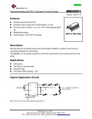
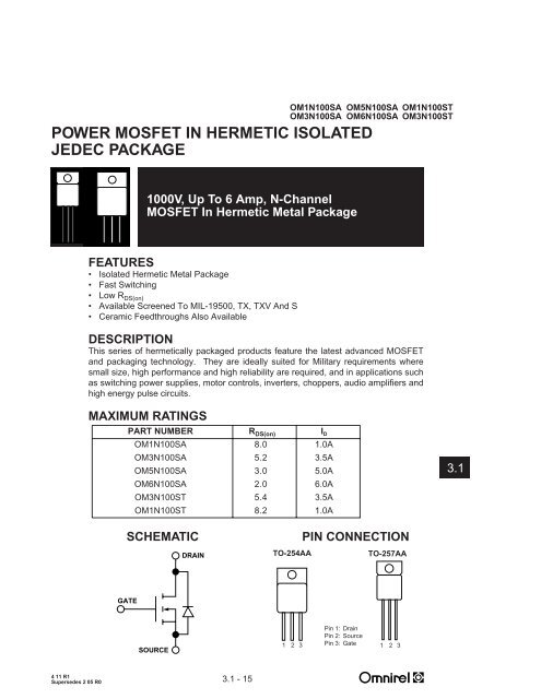
OM1N100SAOM3N100SAOM5N100SAOM6N100SA<strong>POWER</strong> <strong>MOSFET</strong> <strong>IN</strong> <strong>HERMETIC</strong> <strong>ISOLATED</strong><strong>JEDEC</strong> <strong>PACKAGE</strong>OM1N100STOM3N100ST1000V, Up To 6 Amp, N-Channel<strong>MOSFET</strong> In Hermetic Metal PackageFEATURES• Isolated Hermetic Metal Package• Fast Switching• Low R DS(on)• Available Screened To MIL-19500, TX, TXV And S• Ceramic Feedthroughs Also AvailableDESCRIPTIONThis series of hermetically packaged products feature the latest advanced <strong>MOSFET</strong>and packaging technology. They are ideally suited for Military requirements wheresmall size, high performance and high reliability are required, and in applications suchas switching power supplies, motor controls, inverters, choppers, audio amplifiers andhigh energy pulse circuits.MAXIMUM RAT<strong>IN</strong>GSPART NUMBER R DS(on) I DOM1N100SA 8.0 1.0AOM3N100SA 5.2 3.5AOM5N100SA 3.0 5.0AOM6N100SA 2.0 6.0AOM3N100ST 5.4 3.5AOM1N100ST 8.2 1.0A3.1SCHEMATICDRA<strong>IN</strong>TO-254AAP<strong>IN</strong> CONNECTIONTO-257AAGATESOURCEPin 1: DrainPin 2: Source1 2 3 Pin 3: Gate 1 2 34 11 R1Supersedes 2 05 R03.1 - 15
ELECTRICAL CHARACTERISTICS: T C = 25° unless otherwise noted ELECTRICAL CHARACTERISTICS: T C = 25° unless otherwise notedSTATIC P/N OM5N100SA (See Note 3) STATIC P/N OM6N100SA (See Note 3)Parameter Min. Typ. Max. Units Test Conditions Parameter Min. Typ. Max. Units Test ConditionsBV DSS Drain-Source Breakdown 1000 V V GS = 0, BV DSS Drain-Source Breakdown 1000 V V GS = 0,Voltage I D = 250 mA Voltage I D = 250 mAV GS(th) Gate-Threshold Voltage 2.0 4.0 V V DS = V GS , I D = 250 mA V GS(th) Gate-Threshold Voltage 2.0 4.0 V V DS = V GS , I D = 250 mAI GSSF Gate-Body Leakage Forward 100 nA V GS = 20 V, V DS = 0 I GSSF Gate-Body Leakage Forward 100 nA V GS = 20 V, V DS = 0I GSSR Gate-Body Leakage Reverse -100 nA V GS = - 20 V, V DS = 0 I GSSR Gate-Body Leakage Reverse - 100 nA V GS = - 20 V, V DS = 0I DSS Zero Gate Voltage 0.25 mA V DS = Max. Rat., V GS = 0 I DSS Zero Gate Voltage Drain 0.25 mA V DS = Max. Rat., V GS = 0Drain Current 1.0 mA V DS = 0.8 x Max. Rat., Current 1.0 mA V DS = 0.8 x Max. Rat.,V GS = 0, T C = 125° CV GS = 0, T C = 125° CI D(on) On-State Drain Current 5.0 A V DS > I D(on) x R DS(on) Max., I D(on) On-State Drain Current 6.0 A V DS > I D(on) x R DS(on) Max.,V GS = 10 VV GS = 10 VR DS(on) Static Drain-Source On-State 3.0 V GS = 10 V, I D = 2.5 A R DS(on) Static Drain-Source On-State 2.0 V GS = 10 V, I D = 3.0 AResisitance 1 Resistance 1R DS(on) Static Drain-Source On-State 6.0 V GS = 10 V, I D = 2.5 A R DS(on) Static Drain-Source On-State 4.0 V GS = 10 V, I D = 3.0 AResistance 1 T C = 100 C Resistance 1 T C = 100° C3.1 - 17DYNAMICDYNAMICg fs Forward Transductance 4.0 S V DS = 25 V DS(on) , I D = 2.5 A g fs Forward Transductance 4.0 S V DS = 25V, I D = 3.0 AC iss Input Capacitance 2600 pF V GS = 0 C iss Input Capacitance 2600 pF V GS = 0C oss Output Capacitance 350 pF V DS = 25 V C oss Output Capacitance 350 pF V DS = 25 VC rss Reverse Transfer Capacitance 150 pF f = 1 MHz C rss Reverse Transfer Capacitance 150 pF f = 1 MHzT d(on) Turn-On Delay Time 65 ns T d(on) Turn-On Delay Time 65 nst r Rise Time 55 ns t r Rise Time 55 nsT r( V off) Off-Voltage Rise Time 62 ns V DD = 800 V, I D =6AT r (V off ) Off-Voltage Rise Time 62 ns V DD = 800 V, I D = 6At f Fall Time 25 ns R G = 7W, V GS = 10 Vt f Fall Time 25 ns R G = 7W, V GS = 10 VBODY-DRA<strong>IN</strong> DIODE RAT<strong>IN</strong>GS AND CHARACTERISTICSBODY-DRA<strong>IN</strong> DIODE RAT<strong>IN</strong>GS AND CHARACTERISTICSI S Continuous Source Current 6 A Modified MOS<strong>POWER</strong>DI S Continuous Source Current 6 A Modified MOS<strong>POWER</strong>D(Body Diode) symbol showing (Body Diode) symbol showingI SM Source Current 2 G24 A the integral P-N I SM Source Current 2 G24 A the integral P-N(Body Diode) Junction rectifier. S(Body Diode) Junction rectifier.SV SD Diode Forward Voltage 1 2.5 V T C = 25 C, I S = 6 A, V GS = 0 V SD Diode Forward Voltage 1 2.5 V T C = 25 C, I S = 6 A, V GS = 0t rr Reverse Recovery Time 1100 ns I F = I S ,V DD = 100 V t rr Reverse Recovery Time 1000 ns I F = I S ,V DD = 100 Vdl F /ds = 100 A/msdl F /ds = 100 A/ms, T J = 150 C1 Pulse Test: Pulse Width 300msec, Duty Cycle 1.5%. 1 Pulse Test: Pulse Width 300msec, Duty Cycle 1.5%.2 Pulse Width limited by safe operating area. 2 Pulse Width limited by safe operating area.3. Also available in a TO258AA, TO259AA and dual 6 pin Sip, S-6 package 3. Also available in a TO258AA, TO259AA and dual 6 pin Sip, S-6 package3.1OM1N100SA/ST Series
OM1N100SA/ST SeriesABSOLUTE MAXIMUM RAT<strong>IN</strong>GS (T C = 25°C unless otherwise noted)Symbol Parameter OM1N100SA OM3N100SA OM5N100SA OM6N100SA UnitsOM1N100ST OM3N100STI ARAvalanche Current(Repetitive or Non-Repetitive)T j = 25°C 3.5 3.5 6 6 AT j = 100°C 2 2 3.4 3.4 AE AS Single Pulse Avalanche Energy 130 130 850 850 mJStarting T j = 25°C, I D = I AR ,V DD = 25VE AR Repetitive Avalanche Energy 6 6 16 16 mJ(Pulse width limited by T J max, d< 1%)V DS Drain-Source Voltage 1000 1000 1000 1000 VV DGR Drain-Source Voltage (R GS = 20k ) 1000 1000 1000 1000 VI D @ T C = 25°C Continuous Drain Current .50 3.5 5.0 6.0 AI D @ T C = 100°C Continuous Drain Current .30 2.0 3.1 3.7 AI DM Pulsed Drain Current 1 14 14 24 24 AV GS Gate-Source Voltage ±20 ±20 ±20 ±20 VP D @ T C = 25°C Maximum Power Dissipation 90 90 130 130 WP D @ T C =100°C Maximum Power Dissipation 32 32 51 51 WJunction-To-Case Linear Derating Factor .87 .87 2.10 2.10 W/°CJunction-To-Ambient Linear Derating Factor .020 .020 .020 .020 W/°CT JOperating andT stg Storage Temperature Range -55 to 150 -55 to 150 -55 to 150 -55 to 150 °CLead Temperature (1/16" from case for 10secs.) 300 300 300 300 °C1 Pulse Test: Pulse width 300 µsec. Duty Cycle 2%.3.1THERMAL RESISTANCER thJC Junction-To-Case Max. 1.15 1.15 .48 .48 °C/WTO-257AAMECHANICAL OUTL<strong>IN</strong>ETO-254AA.545.200.144 DIA. .535.050.420.190.040.410.045.035.150.140.665.645.537.527.430.410.685.665.800.790.550.530.038 MAX..750.500.005.550.510.005.045.035.150 TYP..260.249.150 TYP..035.025.100 TYP..120 TYP.<strong>PACKAGE</strong> OPTIONSFET 4 FET 3G S D G S DZ-TABDSFET 1G6 P<strong>IN</strong> SIPGSFET 2DDSGFET 1G SDFET 3MOD PAKStandard Products are supplied with glass feedthroughs. For ceramic feedthroughs, add the letter “C” to the part number. Example - OMXXXXCSA<strong>MOSFET</strong>s are also available in Z-Pak, dual and quad pak styles. Please call the factory for more information.205 Crawford Street, Leominster, MA 01453 USA (508) 534-5776 FAX (508) 537-4246