ICP Etching Processes for Nanoimprint Lithograhy
ICP Etching Processes for Nanoimprint Lithograhy
ICP Etching Processes for Nanoimprint Lithograhy

You also want an ePaper? Increase the reach of your titles
YUMPU automatically turns print PDFs into web optimized ePapers that Google loves.
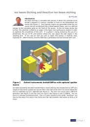
<strong>ICP</strong> Etch <strong>Processes</strong> <strong>for</strong> <strong>Nanoimprint</strong> LithographyC.C.Welch 1 and B.Bilenberg 21 Ox<strong>for</strong>d Instruments Plasma Technology, North End, Yatton, Bristol BS49 4AP, UKTel +44 1934 837000, Fax +44 1934 837001, e-mail colin.welch@oxinst.co.uk2 NIL Technology, Oersteds Plads, DTU Building 347, DK-2800 Kongens Lyngby,Denmark, Tel +45 4525 5828, Fax +45 3972 2722, e-mail: brian.bilenberg@nilt.comIn this paper the application of inductively coupled plasma (<strong>ICP</strong>) etching processes to three criticalsteps in the nanoimprint lithography (NIL) fabrication sequence is demonstrated. <strong>ICP</strong> etching givesexcellent results which meet the stringent demands of NIL technology.Introduction<strong>Nanoimprint</strong> lithography (NIL) is aversatile, cost effective, flexible and highthroughput method <strong>for</strong> fabrication of down toand below 10 nm structures [1] with a widerange of application within e.g. storage [2],optics [3] and bio-sensors [4]. The basic NILsequence is illustrated in Figure 1 whereby theinverse of a stamp pattern is transferred into apolymer on a substrate and subsequentlytransferred into the substrate by dry etching.<strong>Etching</strong> by low pressure of inductivelycoupled plasma (<strong>ICP</strong>) is a familiar means ofpatterning now being increasingly used <strong>for</strong>high quality patterning <strong>for</strong> nanoscale devices.The high ion density, low pressure <strong>ICP</strong> etchregime provides excellent control over etchedprofiles and critical dimension (CD) [5]. <strong>ICP</strong>may be used in three of the critical steps in theNIL sequence (Figure 1) A. <strong>Etching</strong> of thestamp D. Descum of the polymer residual andE. Patterning of the substrate. The suitability of<strong>ICP</strong> <strong>for</strong> these three steps is shown in this paper.ExperimentalSamples <strong>for</strong> fabrication of UV NIL stampshave been provided by NIL Technology,www.nilt.com. 500 µm thick fused silicawafers were prepared with 40 nm sputteredchromium (Cr) and 120 nm ZEP520A [6] highresolution positive resist by spin coating. Thestamp pattern with down to 30 nm structureswas defined by 100 kV EBL (JeolJBX9300FS), dose 220 µC/cm 2 , and developed<strong>for</strong> 2 min in ZEP-N50 [6].<strong>Etching</strong> has been carried out in anOx<strong>for</strong>d Instruments Plasmalab System 100<strong>ICP</strong> tool. This features a cylindrical <strong>ICP</strong> source,independent substrate electrode bias and wideelectrode temperature capability [5].Results and discussionStamp etchThe NIL process must replicate thestructures on the stamp perfectly into thepolymer. Thus, the stamp etch has demandingspecifications regarding sidewall smoothnessand angle, etched protrusion height uni<strong>for</strong>mityand CD control. Ideally the stamp should havea vertical or very slightly tapered sidewall. Are-entrant or trenched profile is undesirable.Figure 1. Schematic of the NIL process.A. A stamp is fabricated in typically silicon orfused silica by electron beam lithography(EBL) and dry etching. B. The stamp ispressed into a soft thermoplastic, thermosettingor UV-curable polymer on a substratecombined with heating or UV radiation CPolymer cured and stamp released fromsubstrate D. Residual imprint polymer understamp protrusions removed by ‘descum’process E. Imprinted pattern transferred intosubstrate by dry etching.Figure 2. SEM image of optimized fused silicastamp etch (30nm features to 200nm depth)
]An octofluorocyclobutane (C 4 F 8 )-oxygen(O 2 ) mixture was used <strong>for</strong> <strong>ICP</strong> etching of fusedsilica. Figure 2 shows an optimized stampetch. 30nm features have been etched to200nm depth at a uni<strong>for</strong>m rate of 85nm/minwith selectivity over a Cr mask >200:1. Theprofile is vertical and trench free. Figure 3shows profile control by temperature.Trenching is an effect often seen <strong>for</strong> ion-drivenprocesses such as silica etching and ismanifested as deeper etching at the base of thesidewalls. Figure 3 also shows how trenchingmay be eliminated by reducing DC bias. <strong>ICP</strong>has the benefit of DC bias control largelyindependent of the other process parameters.is a room temperature process using a C 4 F 8 -SF 6 gas mixture (Figure 5). The second is thecryogenic process using a SF 6 -O 2 gas mixture(Figure 6). Control of silicon etched profile bymeans of the <strong>ICP</strong> process parameters is shown.Profile [degree95939189878560 65 70 75C4F8 %in SF6Fig.5 16nm Si lines etched by C 4 F 8 -SF 6 <strong>ICP</strong>process. Profile control by C 4 F 8 % (right)94Profile [degrees]94929088868425 35 45 55 65Temperature [°C]Trench% of silica depth1210864200 50 100 150 200 250DC bias [-V]Figure 3. Control of profile (left) and trenching(right) <strong>for</strong> fused silica stamp <strong>ICP</strong> etch.DescumAfter imprinting there is inevitably someresidual polymer under the stamp protrusions,typically 10-20 nm thick <strong>for</strong> stamp protrusionheights of 100-200 nm. Be<strong>for</strong>e final patterntransfer this residual must be removed withuni<strong>for</strong>m and minimized CD and profile changeof the features. <strong>ICP</strong> processing succeeds byenabling stable low pressure and henceanisotropic conditions. Cooling of thesubstrate also improves anisotropy. Figure 4shows a good descum of a polystyrene residual(25% of protrusion height). The process usespure O 2 and removes 200nm of residual in2minutes with negligible CD loss.Figure 4. Descum of polystyrene pattern onquartz. CD constant at 350 nm be<strong>for</strong>e (left) andafter (right) descum.Nanoscale substrate etchThe requirements to the final substrateetch depend on the application and so aremuch more diverse than the stamp etch anddescum. Examples are given of two <strong>ICP</strong>silicon etch processes with complementaryattributes <strong>for</strong> nanoscale etching [7]. The firstProfile [degree]9290888684-105 -110 -115 -120Temperature [°C]Figure 6. 1µm deep Si lines with 10:1 aspectratio etched by <strong>ICP</strong> cryo processProfile control by temperature (right)ConclusionsThe use of <strong>ICP</strong> <strong>for</strong> three etching steps in atypical NIL process scheme has beendemonstrated. The <strong>ICP</strong> etch shows superiorcapabilities regarding etching of highper<strong>for</strong>mance NIL stamps with well controlledprofiles. The stable low pressure descumprocess possible with <strong>ICP</strong> effectively removesthe residual polymer after imprinting withminimal loss of CD and <strong>ICP</strong> is also perfect <strong>for</strong>transferring the imprinted pattern into fusedsilica and silicon.References[1] S. Y. Chou et al. J. Vac. Sci. &Technol. B 15 (1997) 2897.[2] T. Glinsner et al. Solid State Technology48 (2005) 51.[3] M. B. Christensen et al. Optics Express 15(2007) 3931.[4] B. Bilenberg et al. Microelectronic Eng. 83(2006) 1609.[5] A.L.Goodyear, D.L. Oylnick et al.J.Vac.Sci.Technol. B 18 6 (2000). 3471.[6] Zeon corporation Tokyo Japanwww.zeon.co.jp[7] C.C.Welch et al.Microelectronic Engineering Volume 83,Issues 4-9, April-September 2006, 1170.