1. Basic Concepts in Reliability Design - nl3prc
1. Basic Concepts in Reliability Design - nl3prc
1. Basic Concepts in Reliability Design - nl3prc

Create successful ePaper yourself
Turn your PDF publications into a flip-book with our unique Google optimized e-Paper software.
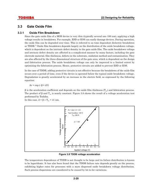
[2] <strong>Design</strong><strong>in</strong>g for <strong>Reliability</strong>3.3 Gate Oxide Film3.3.1 Oxide Film BreakdownS<strong>in</strong>ce the gate oxide film of a MOS device is very th<strong>in</strong> (typically several nm∼100 nm), apply<strong>in</strong>g a highvoltage results <strong>in</strong> breakdown. For example, ESD or EOS can easily damage devices. Dur<strong>in</strong>g operation,the oxide film can be degraded over time. This is referred to as time dependent dielectric breakdownor TDDB. 7) Oxide film breakdown depends largely on the distribution of the oxide breakdown voltage,which is dependent on the <strong>in</strong>tr<strong>in</strong>sic defect density <strong>in</strong> the gate oxide film. The oxide breakdown voltageand <strong>in</strong>tr<strong>in</strong>sic defect density are affected <strong>in</strong> a complicated manner by many factors, <strong>in</strong>clud<strong>in</strong>g the gateelectrode material, film thickness, defects <strong>in</strong> the substrate, oxidation method and contam<strong>in</strong>ation. Theyare also affected by the three-dimensional structure of the gate area, which is dependent on the designand fabrication process. The oxide breakdown voltage can only be improved to a limited extent byoptimiz<strong>in</strong>g the fabrication process. Hence, protective circuits are added to prevent ESD or EOS.In the case of TDDB, add<strong>in</strong>g protective circuits is not effective because the breakdown of the oxide filmoccurs over a period of time, even if the device is operated below the typical oxide breakdown voltage.Degradation is greatly accelerated by an <strong>in</strong>crease <strong>in</strong> the electric field, as expressed by the follow<strong>in</strong>gequation:Av = exp (−β ∆V)β is the acceleration coefficient and depends on the oxide film thickness (T ox ) and fabrication process.The product of β and T ox is nearly constant. Figure 3.8 shows the result of a voltage acceleration testperformed by Toshiba.In this case, d = β × T ox = 41 nm.Av = exp (−β ∆V)Test Condition: 125°CT ox : 250 ÅVoltage accelerationfactorβ = <strong>1.</strong>655.0 5.5 6.0 6.5 7.0 7.5 8.0 8.5 9.0 9.5Applied voltage (V)Figure 3.8 TDDB voltage accelerationThe temperature dependence of TDDB is not thought to be large and its failure distribution is knownto be logarithmic. It has also been found that the TDDB failure rate depends greatly on the process,exhibit<strong>in</strong>g higher rates for processes with a more dispersed oxide breakdown voltage distribution.Such process dispersions are considered to be caused by lot-to-lot variations.2-20