Adder Circuits
Adder Circuits
Adder Circuits

You also want an ePaper? Increase the reach of your titles
YUMPU automatically turns print PDFs into web optimized ePapers that Google loves.
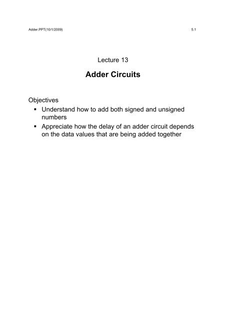
<strong>Adder</strong>.PPT(10/1/2009) 5.1Lecture 13<strong>Adder</strong> <strong>Circuits</strong>Objectives• Understand how to add both signed and unsignednumbers• Appreciate how the delay of an adder circuit dependson the data values that are being added together
<strong>Adder</strong>.PPT(10/1/2009) 5.2Full <strong>Adder</strong>PQS+PQCICICCSOutput is a 2-bit number counting how many inputs arehighP Q CI C S0 0 0 0 00 0 1 0 10 1 0 0 10 1 1 1 01 0 0 0 11 0 1 1 01 1 0 1 01 1 1 1 1C P Q P CI Q CIS P Q CI• Symmetric function of the inputs• Self-dual: Invert all inputs invert all outputsIf k inputs high initially then 3–k high when invertedInverting all bits of an n-bit number make x 2 n –1–x• Note: P Q CI = (P Q) CI = P (Q CI)
<strong>Adder</strong>.PPT(10/1/2009) 5.3Full <strong>Adder</strong> Circuit9-gate full-adder NAND implementation (do not memorize)PQCICSPropagation delays:From To DelayPQorCI P,Q S 3P,Q or CI C 2Complexity: 25 gate inputs 50 transistors but use ofComplexity: 25 gate inputs 50 transistors but use ofcomplex gates can reduce this somewhat.
<strong>Adder</strong>.PPT(10/1/2009) 5.4N-bit adderWe can make an adder of arbitrary size by cascading fulladder sections:P0Q0C–1PQCISCP1 P2 S0 P S1 P S2Q1 S Q2 SQQC0 C1 C2CI CCI CP3Q3PQCISCS3C3The main reason for using 2’s complement notation forsigned numbers is that:Signed and unsigned numbers can use identical circuitryP0P1P2P3Q0Q1Q2Q30303PQ03S0S1S2S3C–1CIC3C3
<strong>Adder</strong>.PPT(10/1/2009) 5.5<strong>Adder</strong> Size SelectionThe number of bits needed in an adder is determined bythe range of values that can be taken by its output.If we add two 4-bit numbers, the answer can be in therange:• 0 to 30 for unsigned numbers• -16 to +14 for signed numbersIn both cases we need a 5-bit adder to avoid anypossibility of overflow:P0P1P2P3Q0Q1Q2Q3?040PQ04S0S1S2S3S4?40C–1CIC4C4We need to expand the input numbers to 5 bits. How dowe do this ?
<strong>Adder</strong>.PPT(10/1/2009) 5.6Unsigned numbersExpanding Binary NumbersExpand an unsigned number by adding the appropriatenumber of 0’s at the MSB end:5 0101 0000010113 1101 00001101Signed numbersExpand a signed number by duplicating the MSB theappropriate number of times:5 0101 00000101–3 1101 11111101This is known as sign extensionUnsignedShrinking Binary NumbersCan delete any number of bits from the MSB end so longas they are all 0’s.SignedCan delete any number of bits from the MSB end so longas they are all the same as the MSB that remains.
<strong>Adder</strong>.PPT(10/1/2009) 5.7Adding Unsigned NumbersTo avoid overflow, we use a 5-bit adder:P0P1P2P3Q0Q1Q2Q30040PQ04S0S1S2S3S4040C–1CIC4C4The MSB stage is performing the addition: 0 + 0 + C3.Thus S4 always equals C3 and C4 always equals 0.P0P1P2P3Q0Q1Q2Q30303PQ03S0S1S2S3S40C–1CIC3C3We can use a 4-bit adder with C3 as an answer bit.
<strong>Adder</strong>.PPT(10/1/2009) 5.8Adding Signed NumbersTo avoid overflow, we use a 5-bit adder:P0P1P2P3Q0Q1Q2Q3040PQ04S0S1S2S3S440C–1CIC4C4This is different from the unsigned case because P4 andQ4 are no longer constants. We cannot simplify this circuitby removing the MSB stage.If P and Q have different signs then S4 will not equal C3.e.g. P=0000, Q=1111Unsigned P+Q=01111 01111, Signed P+Q=11111Some minor simplifications are possible:• If the C4 output is not required, the circuitry thatgenerates it can be removed.• S4 can be generated directly from P3, Q3 and C3which reduces the circuitry needed for the last stage.
<strong>Adder</strong>.PPT(10/1/2009) 5.9<strong>Adder</strong> Propagation DelayP0Q0C–1PQCISCP1 P2 S0 P S1 P S2Q1 S Q2 SQQC0 C1 C2CI CCI CP3Q3PQCISCS3S4P0C0 C0 C1 C1 C2 C2 S32 2 2 3Delays within each stage (in gate delays):P, Q, CI S = 3 P, Q, CI C = 2Worst-case delay is:P0 C0 C1 C2 S3 = 3×2 + 3 = 9Note:WealsohaveQ0 S3 = 9 and C–1 S3 = 9For an N-bit adder, the worst delay is (N–1)×2 + 3 = 2N+1Example of worst case delay:• Initially: P3:0=0000, Q3:0=1111 S4:0=01111• Change to: P3:0=0001, Q3:0=1111 S4:0=10000
<strong>Adder</strong>.PPT(10/1/2009) 5.10Delays are Data-DependentTo determine the delay of a circuit, we need to specify:1. The circuit2. The initial value of all the inputs3. Which of the inputs changesExample: What is the propagation delay AQ ?AYXQBZAnswer 1 (B=0):• Initially: A=0, B=0 X=1, Y=0, Z=0, Q=0• Then: A Y Q 2 gate delaysAnswer 2 (B=1):• Initially: A=0, B=1 X=1, Y=0, Z=1, Q=1• Then: A X Z Q 3 gate delays
<strong>Adder</strong>.PPT(10/1/2009) 5.11Worst-Case DelaysWe are normally interested only in the worst-case delayfrom a change in any input to any of the outputs.The worst-case delay determines the maximum clockspeed in a synchronous circuit:CLOCKC1C1W1DXLogicY1DZCLOCKWXYZtime 0 tp tp+tg Ttp + tg + ts < TSince the clock speed must be chosen to ensure that thecircuit always works, it is only the worst-case logic delaythat matters.
<strong>Adder</strong>.PPT(10/1/2009) 5.12Quiz1. In an full adder, why is it normally more important toreduce the delay from CI to C than to reduce thedelay from P to S ?2. How many bits are required to represent the numberA+BifAandBare(a)8-bit A B are unsigned numbers oralternatively (b) 8-bit signed numbers.3. How do you convert a 4-bit signed number into an 8-bit signed number ?4. How do you convert a 4-bit unsigned number into an8-bit signed number ?5. How is it possible for the propagation delay of a circuitfrom an input to an output to depend on the value ofthe other inputs ?
<strong>Adder</strong>.PPT(10/1/2009) 5.13Lecture 14Fast <strong>Adder</strong> <strong>Circuits</strong> (1)Objectives• Understand how the propagation delay of an addercan be reduced by inverting alternate bits.• Understand how the propagation delay of an addercan be reduced still further by means of carrylookahead.
<strong>Adder</strong>.PPT(10/1/2009) 5.14Standard N-bit <strong>Adder</strong>Delay of standard N-bit adder = 2N+1P0Q0C–1PQCISCP1 P2 S0 P S1 P S2Q1 S Q2 SQQC0 C1 C2CI CCI CP3Q3PQCISCS3S4P0C0 C0 C1 C1 C2 C2 S32 2 2 3Delay of carry path within each full adder = 2Carry path consists of three 2-input + one 3-input NANDs
<strong>Adder</strong>.PPT(10/1/2009) 5.15Faster <strong>Adder</strong> <strong>Circuits</strong>: 1Because a full-adder is self-dual, it will still work if foralternate stages we invert both the inputs and the outputs:Full <strong>Adder</strong>P11 1S1Q11P1P0Q0C–1PQCISCP2 S0P S1P S2Q1 SQ2 SQQC0 C0C1 C1C2CI CCI C1 1Now consider only the Carry signals:P0Q0P1Q1C1aP2Q2C0C1bC1C2C–11C0C1c1C1<strong>Adder</strong> Stage 0 <strong>Adder</strong> Stage 1 <strong>Adder</strong> Stage 2By merging the shaded gates we can reduce the delay toone gate per adder stage.
<strong>Adder</strong>.PPT(10/1/2009) 5.16Fast <strong>Adder</strong> <strong>Circuits</strong>: 1 (part 2)C0aC0bC0cC0P1Q1C1aC1bP1Q1C0aC0bC0cC1aC1b1C0C1cC1cWe can merge the 3-NAND and inverter into the finalcolumn of gates as shown; this gives one delay per stage:P1P2Q1 Q2 P0Q0C0aC0bC0cC1aC1bC1cC2aC2bC2cC–1C1<strong>Adder</strong> Stage 0 <strong>Adder</strong> Stage 1 <strong>Adder</strong> Stage 2The signals C1a, C1b, C1c form an AND-bundle: C1 is trueonly if all of them are high. We don’t need the signal C1directly so the shaded gate can be omitted.
<strong>Adder</strong>.PPT(10/1/2009) 5.17Fast <strong>Adder</strong> <strong>Circuits</strong>: 1 (part 3)Even stages:Delays:PQCIa,b,cCOa,b,cP,Q,CI S 3P,Q,CI C 1S30 gate inputs 60 transistorsOdd stages:Delays:P,Q S 5P,Q C 2CI S 4CI C 1PQCIa,b,c11COa,b,c1S33 gate inputs 66 transistorsBundles are denoted by a single wire with a / through it.22% more transistors but twice as fast.
<strong>Adder</strong>.PPT(10/1/2009) 5.18Fast <strong>Adder</strong> <strong>Circuits</strong>: 1 (part 4)For an N-bit adder we alternate the two modules (with anormalish first stage):P0Q0C–1PQCISCP1 P2 S0 P S1 P S2Q1 S Q2 SQQC0 C1 C2CI CCI CP3Q3PQCISCS3C3S4P01C0P1C021C1C1C11C2C2C24S32S4Worst case delay is:P0 !C0 C1 !C2 S3 = 7 gate delaysNote that:• Delay to S4 is shorter than delay to S3• Delay from P1 is the same as delay from P0• Worst-case example:Initially: P3:0=0000, 0000, Q3:0=1111, then P0Delay for N-bit adder (N even) is N+3(compare with 2N+1 for original circuit)
<strong>Adder</strong>.PPT(10/1/2009) 5.19Carry Lookahead (1)For each bit of an N-bit adder we get a carry out (CO=1) iftwo or more of P,Q,CI are equal to 1.There are three possibilities:• P,Q=00: C=0 always Carry Inhibit• P,Q=01 or 10: C=CI Carry Propagate• P,Q=11: C=1 always Carry GenerateWe define three signals:• CG = P • Q Carry Generate• CP = P Q Carry Propagate• CGP = P + Q Carry Generate or PropagateWe get a carry out from a bit position either if that bitgenerates a carry (CG=1) or else if it propagates the carryand there is a carry in from the previous bit (CP•CI CI = 1):C = CG + CP•CISince CGP = CG + CP, an alternate expression is:C = CG + CGP•CICIThe second expression is usually used since P + Q iseasier and faster to generate than P Q.
<strong>Adder</strong>.PPT(10/1/2009) 5.20Carry Lookahead (2)Consider all the ways in which we get a carry out of bitposition 3:1) Bit 3 generates a carry: 1???+ 1???2) Bit 2 generates a carry and 11??bit 3 propagates it. + 01??3) Bit 1 generates a carry and 101?bit 2 propagates it and + 011?bit 3 propagates it.4) Bit 0 generates a carry and 1011bit 1 propagates it and + 0101bit 2 propagates it andbit 3 propagates p it.5) The C–1 input is high and 1011bits 0,1,2 and 3 all propagate the carry. + 0100 +1ThusC3 = CG3 + CP3•CG2 + CP3•CP2•CG1 +CP3•CP2•CP1•CG0+CP3•CP2•CP1•CP0•C–1As before, we can use CGPn in place of CPn.
<strong>Adder</strong>.PPT(10/1/2009) 5.21Carry Lookahead (3)Each stage must now generate CP and CGP instead of C:P0Q0C–1 S0 P1 S1 P2 S2 P3 S3P SP SP SP SQ1Q2Q3QCGP CGP0 QCGP CGP1 QCGP CGP2 QCGP CGP3C1CICG CG0 C0CICG CG1 CICG CG2 C2CICGCG3Logic Logic LogicTo laterstagesC 0 =CG 0 +CGP 0 •C –1C 1 = CG 1 + CGP 1 •CG 0 + CGP 1 •CGP 0 •C –1C 2 = CG 2 + CGP 2 •CG 1 + CGP 2 •CGP 1 •CG 0 +CGP 2 •CGP 1 •CGP 0 •C –1Worst-case propagation delay:P0 CG0 = 1 gate delay (CG0 = P0•Q0)CG0 C2 = 2 gate delays (see above expression)C2 S3 = 3 gate delays (from full adder circuit)Total = 6 gate delays (independent of adder length)
<strong>Adder</strong>.PPT(10/1/2009) 5.22Carry Lookahead (4)Carry lookahead circuit complexity for N-bit adder:• Expression for Cn involves n+2 product terms eachcontaining an average of ½(n+3) input signals.• Direct implementation of equations for all N carrysignals involves approx N 3 /3 transistors.N = 64 N 3 /3 = 90,000• By using a complex CMOS gate, we can actuallygenerate Cn using only 4n+6 transistors so all Nsignals require approx 2N 2 transistors.N = 64 2N 2 = 8,000Actual gain is not as great as this because for large n,the expression for Cn is too big to use a single gate.• C–1, CG0 and CGP0 must drive N–1 logic blocks. Forlarge N we must use a chain of buffers to reduce delay:CG0 To 81 1 1 1logicblocksThe circuit delay is thus not quite independent of N.
<strong>Adder</strong>.PPT(10/1/2009) 5.23Quiz1. What does it mean to say that a full-adder is self-dual?2. How does placing an inverter between each stage of amulti-bit adder allow the merging of gates inconsecutive stages ?3. In a 4-bit adder, give an example of a propagationdelay that increases when alternate bits are inverted.4. Why is a carry-lookahead adder generallyimplemented using CGP rather than CP outputs ?
<strong>Adder</strong>.PPT(10/1/2009) 5.24Lecture 15Fast <strong>Adder</strong> <strong>Circuits</strong> (2)Objectives• Understand the carry skip technique for reducing thepropagation delay of an adder circuit.• Understand how the carry save technique can beused when adding together several numbers.Summary So Far:• Cascading full adders:2N+1 gate delays, 50N transistors• Use self-duality to invert odd-numbered stages:N+3 gate delays, 61N transistors• Carry lookahead:6 gate delays, between ee 2N 2 and 0.3N 3 transistors ta sstos
<strong>Adder</strong>.PPT(10/1/2009) 5.25Consider a 12-bit adder:Carry Skip (1)P0,Q0 P2,Q2 P4,Q4 P6,Q6 P8,Q8 P10,Q10P1,Q1 P3,Q3 P5,Q5 P7,Q7 P9,Q9 P11,Q11 C–1 C11S0 S1 S2 S3 S4 S5 S6 S7 S8 S9 S10 S11The worst-case delay path is from C–1 1toS11S11.In carry skip, we speed up this path by allowing the carrysignal to skip over several adder stages at a time:P0,Q0 P2,Q2 P4,Q4 P6,Q6 P8,Q8 P10,Q10P1,Q1 P3,Q3 P5,Q5 P7,Q7 P9,Q9 P11,Q11 C–1 C11S0 S1 S2 S3 S4 S5 S6 S7 S8 S9 S10 S11
<strong>Adder</strong>.PPT(10/1/2009) 5.26Carry Skip (2)Consider our fast adder circuit without carry lookahead (butusing alternate-bit inversion):P0Q0C–1PQCISCP1 P2 S0 P S1 P S2Q1 S Q2 SQQC0 C1 C2CI CCI CP3Q3PQCISCS3C3P0C–111C0C0P1C02C1C241C1 C11C2C21S3C3There are two possible sorts of addition sum:• All bits propagate p the carry C 3 = C –1 :0101 01011010 10100 101111 10000C –1 C 3 = 4 gate delays• At least one bit doesn’t propagate the carry C 3 is completely independent of C –1 :0101 01011110 11100 110011 10100C –1 C 3 = 0 gate delays
<strong>Adder</strong>.PPT(10/1/2009) 5.27Carry Skip (3)We speed up C–1 C3 by detecting when all bits propagatethe carry and using a multiplexer to allow C–1 to skip all theway to C3:P0Q0C–1PQCICPSCCP0CP1CP2CPCPS0P1P2P S1 PQ1 S Q2QQSS2C0CI CC1CI CC2P3Q3PQCICPSCCP3S3C3MUXG11CSKC3X1P0P0C–1211CP0C0C0P1C024C1C21C1C11C2C21S3C3CSKC3XC–1211C3XC3XC3XCalculate Carry Propagate (CP = P Q) for each bit. Callthis 2 gate delays since XOR gates are slow. CSK=1 ifallbits propagate the carry.• Case 1: All bits propagate the carryC–1 !C3X = 1 gate delay (via multiplexer)• Case 2: At least one bit inhibits or propagates the carry C–1 does not affect C3Longest delays to !C3X and S3:• P0 !C3X = 5 (via either !C0 or CSK)• P0 S3 = 7
<strong>Adder</strong>.PPT(10/1/2009) 5.28Multiplexer DetailsCarry Skip (4)CSKC3C–1MUXG111C3XCSK!C3X0 !C31 !C–1CSK1C3C3C3XC–1C–1We merge both AND gates:• the 3-AND gate merges into the following NAND• the 2-AND gate merges into the next adder stageCSK1C3C–1C3XC–1 C–1 !C3X now equals 1 gate delay.
<strong>Adder</strong>.PPT(10/1/2009) 5.29Carry Skip (5)Combine 4 blocks to make a 16-bit adder:P3:0Q3:0P3:0Q3:0S3:0S3:0P7:4Q7:4P3:0Q3:0S3:0S7:4P11:8Q11:8P3:0Q3:0S3:0S11:8P15:12Q15:12P3:0Q3:0S3:0S15:12C–1CIC3XC3CIC3XC7CIC3XC11CIC3XC15P0C–151C3C3C31C7C71C11P12C1177S15S15Worst-case delay is:P0 !C3 C7 !C11 S15 = 14 gate delaysEach additional block of 4 bits gives a delay of only 1 gatedelay: this corresponds to ¼ gate delay per bit.For an N-bit adder we have a delay of ¼N+10. We canreduce this still further by having larger super-blocks.Carry circuit delays:Simple 2N+1Bit-inversion N+3Carry Skip ¼N+10Carry Lookahead 6• but lots of circuitry and high gate fanout more delay
<strong>Adder</strong>.PPT(10/1/2009) 5.30Adding lots of numbersIn multiplication circuits and digital filters we need to addlots of numbers together.Suppose we want to add together five four-bit unsignednumbers: V, W, X, Y and Z.V3:0W3:0X3:0Y3:0Z3:0DEFSIf we use carry-lookahead adders, each stage will have 6gate delays.Total delay to add together K values will be (K–1) × 6.Thus K=16 gives a delay of 90 gate delays.
<strong>Adder</strong>.PPT(10/1/2009) 5.31Addition TreeIn practice we use a tree arrangement of adders:SNumber of values, K 16 8 4 2 1log 2(K) 4 3 2 1 0Each column of adders adds a delay of 6 and halves thenumber of values needing to be added together.Equivalently, each column of adders reduces log 2 K by one.Hence the total delay is is log 2 K × 6 giving a delay of 24 toadd together 16 values.The total number of adders required is still K–1 as before.
<strong>Adder</strong>.PPT(10/1/2009) 5.32Carry-Save <strong>Adder</strong>Take a normal 4-bit adder but don’t connect up thecarrys:P0Q0R0PQCISCP1 P2 P3S0 P S1 P S2Q1 S Q2 S Q3QQC0 R1 C1 R2 C2 R3CI CCI CPQCISCS3C3We have P+Q+R = 2C + SE.g. P=9, Q=12, R=13gives C=13, S=8We call this a carry-save adder: itreduces the addition of 3 numbers tothe addition of 2 numbers.The propagation delay is 3 gatesregardless of the number of bits. Theamount of circuitry is much less thana carry-lookahead adder.P:Q:R:S:C:10011100110110001101_PQRCSSCThe circuit reduces log 2 K by 0.585 (from 1.585 to 1.0)for a delay of 3. The overall delay we can expect istherefore log 2 K × 3/0.585 = log 2 K × 5.13. This is betterthan carry lookahead for less circuitry.
<strong>Adder</strong>.PPT(10/1/2009) 5.33Carry Save ExampleWe will calculate: 13+10+5+11+12+1 = 52CSA P GSB QHC R C ×2CSD P ISE QJF R C ×2CSPSQR CLK×2CSPSQRCNM×2PQSXA:B:C:G:H:11011010010100101101_ _G:2H:I:K:L:_00101 101__01101 1110_ 0010_ _M:2N:X:010001011__0110100D:E:F:I:J:10111100000101101001_K:2L:2J:M:N:111100010_1001_010001011__Notes:1. ×2 requires no logic: just connect wires appropriately2. No logic required for adder columns with only 1 input3. All adders are actually only 4 bits wide4. Final addition M+2N requires a proper adder
<strong>Adder</strong>.PPT(10/1/2009) 5.34Carry-Save TreeWe can construct a tree to add sixteen values together:CSCSCSCSCSCSCSCSCSCSCSCSCSCSSNumber ofvalues, K16 13 9 6 4 3 2 1log 2(K) 4 3.7 3.17 2.58 2 1.58 1 0Delay 0 3 6 9 12 15 18 24Delay/log 2(K) 10 5.65 5.13 5.13 7.23 5.13 6• The final stage must be a normal adder because weneed to obtain a single output.• The delay is the same as for a conventionallookahead-adder tree but uses much less circuitry.• The irregularity of the tree causes a reduction inefficiency but this is relatively small (and becomeseven smaller for large K).• Inverting alternate stages will speed up both treecircuits still further but requires more circuitry.
<strong>Adder</strong>.PPT(10/1/2009) 5.35Merry ChristmasThe End
<strong>Adder</strong>.PPT(10/1/2009) 5.36Quiz1. Ina4bit 4-bit adder, how can you tell from P0:3 and Q0:3whether or not C3 is dependent on C–1 ?2. A multiplexer normally has 2 gate delays from its datainputs to its output. How is this reduced to 1 gate delayin the carry skip circuit ?3. If five 4-bit numbers are added together, how manybits are needed to represent the result ?