Low Noise Avalanche Photodiodes
Low Noise Avalanche Photodiodes
Low Noise Avalanche Photodiodes
- No tags were found...

Create successful ePaper yourself
Turn your PDF publications into a flip-book with our unique Google optimized e-Paper software.
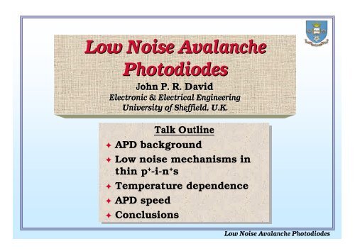
<strong>Low</strong> <strong>Noise</strong> <strong>Avalanche</strong><strong>Photodiodes</strong>John P. R. DavidElectronic & Electrical EngineeringUniversity of Sheffield, U.K.Talk Outline✦ APD background✦ <strong>Low</strong> noise mechanisms in inthin p + + -i-n + + s✦ Temperature dependence✦ APD speed✦ Conclusions<strong>Low</strong> <strong>Noise</strong> <strong>Avalanche</strong> <strong>Photodiodes</strong>
National Centre for III-V Technologies,University of Sheffield, UK180 miles★ Established in in Department of of Electronic &Electrical Engineering, University of ofSheffield in in 1978 1978★ Mission: To To provide III-V wafers &devices to to the the UK UK academic community★ Current Capability: 2 MBE, 3 MOVPE,Device Fabrication, Characterisation★ Staff: 10 10 scientists, 6 technicians★ Growth output: 750 750 wafers/year★ Optical wafers & devices: Lasers, LEDs,VCSELs, RC-LEDs, waveguides,modulators, AFPMs, pins, APDs, Q-Dotlasers, Q-Cascade lasers★ Electrical wafers & devices: HBTs,HEMTs, diodes<strong>Low</strong> <strong>Noise</strong> <strong>Avalanche</strong> <strong>Photodiodes</strong>
Generic communication systeminputdataTransmitterSignalcarryingmediumReceiveroutputbits/sRepeaterspacing X kmCommunication capacity - Bit rate length product= repeater spacing*data rate {X [km]*Bandwidth [b/s]}Using an APD can increaserepeater spacing<strong>Low</strong> <strong>Noise</strong> <strong>Avalanche</strong> <strong>Photodiodes</strong>
p-i-n vs. APDPhotocurrentp-i-noperatingrangeAPDoperatingrangeReverse Bias Voltagep-i-nlow voltagebias insensitivetemperatureinsensitivesimple bias circuitfastsimple bias circuitcheap✽✽✽✽✽✽✽APD✽ high sensitivity✽ single photon detection(possibility)<strong>Low</strong> <strong>Noise</strong> <strong>Avalanche</strong> <strong>Photodiodes</strong>
Technology ComparisonPhotomultipliers<strong>Avalanche</strong>photodiodes+ High gain (~10 6 )+ <strong>Low</strong> dark current+ <strong>Low</strong> noise? Reliability+ Inexpensive+ Compact+ Rugged+ High detectivity+ High reliability+ Simpler, cheaper filters+ Reasonable gain+ High efficiency+ <strong>Low</strong> voltage (
Comparison of three detector typesPIN-FET Ge APD InGaAs APDSensitivity X dBm (X+4) dBm (X+8) dBmCost Moderate Moderate HighWavelength 1.3mm & 1.5mm 1.3mm 1.3mm & 1.5mmReliability 10 11 hrs 10 6 hrs 10 6 hrsu An InGaAs APD requires 8dB less opticalpower to produce the same signal as a PIN-FET.u PIN-FET is cheaper, faster and more reliable.<strong>Low</strong> <strong>Noise</strong> <strong>Avalanche</strong> <strong>Photodiodes</strong>
p-i-n vs. APDComparison of sensitivitySensitivity ( (dBm dBm)ð APDs can have anextra -8dBmsensitivity c.f. p-i-nð APD advantagereduces as as speedincreasesBit Rate (GB/s)<strong>Low</strong> <strong>Noise</strong> <strong>Avalanche</strong> <strong>Photodiodes</strong>
InGaAs/InP SAM-APD<strong>Low</strong> <strong>Noise</strong> <strong>Avalanche</strong> <strong>Photodiodes</strong>
APD VendorsVendors Sensitivity V BD (V) D V BD (V/ C) 3DB bandwidth Misc:(dBm)(GHz)JDSU ERM577 -32 40-70 1.8 10nA@ V BD -1.58.5uA/uW@ V BD -1.5Mitsubishi-33 35-75 0.12 1.9FU319SPAAgere-34 45-70 0.07-0.14 2P173AFujitsu-34 50 0.12 2.5FRM5W232BSNova Crystals - 29-32 0.03 Fused InGaAs/SiNVR251NEC 8501 40-80 0.1 3 7nA@0.9 V BDAlcatel 1914 30-75 3.5 70nA@0.9 V BDSensors Unlimited -24 25-42 6 5nA@ V BD -1SU-10ATRMitsubishi-25 20-40 0.05 7FU321SPAJDSU ERM578 -22 20-40 7NEC 4270 -25 16-32 0.02 8 Superlattice APD(k=0.4)<strong>Low</strong> <strong>Noise</strong> <strong>Avalanche</strong> <strong>Photodiodes</strong>
Ionization - Threshold energyFor ionization:1) energy and momentum conservation2) minimisation of energyImpact ionization schematicdiagramvalence electronholefinal electronEghot electronE thm em hhm s-om lhE g = Band gapE th = Threshold energy‘minimum energy forionization’For parabolic bandsand equal masses,E th = 1.5 E g<strong>Low</strong> <strong>Noise</strong> <strong>Avalanche</strong> <strong>Photodiodes</strong>
Multiplication processtimeMultiplication buildup timerequired to achieve M1injectedelectronHigh field region7collectedelectronsM e = 7✪ Multiplication=current out/current in in✪ <strong>Avalanche</strong> takes timeto to build-upelectronhole<strong>Low</strong> <strong>Noise</strong> <strong>Avalanche</strong> <strong>Photodiodes</strong>
Excess avalanche noiseMean Multiplication, 35302520151050Multiplication buildup timerequired to achieve MMean Multiplication <strong>Noise</strong> on Multiplication0 10 20 30 40 50 60‣ An APD can give us usgain.‣ Unfortunately theavalanche noise candegrade the S/N ratio.‣ An optimum value for exists.Reverse bias in Volts<strong>Low</strong> <strong>Noise</strong> <strong>Avalanche</strong> <strong>Photodiodes</strong>
An ideal avalanche photodiodeIphotonoise current=2eIBphotoAPDbiasedto Gain = MMIphotoMean Square<strong>Noise</strong> current=2eIBMphoto2✏Non ideal APDS = 2eI photo photoBM 2 Fwhere F = excess noise factor✏For an ideal APD F = 1<strong>Low</strong> <strong>Noise</strong> <strong>Avalanche</strong> <strong>Photodiodes</strong>
BackgroundLog (Power)Mean multiplicationIdealRealReverse bias voltageAPD signalAPD noiseOptimumSNRPreamplifiernoise floorM=1 M optMultiplication factor➲ APD’s rely rely on on internalgain to to improve S/N S/N ratio➲ Impact ionization processstochasticavalanchenoise➲ Excess avalanche noiselimits APD’s maximumuseful gain, M➲ In In bulk structure, largeb/a b/a (or (or a/b) ratio requiredfor for low low excess noise<strong>Low</strong> <strong>Noise</strong> <strong>Avalanche</strong> <strong>Photodiodes</strong>
Photodetectors - S/Np-i-n photodiode and amplifierI ph__i 2 AMPA[W] V o( Iph)S=Nequiv. amp. noisesource( i )amp22<strong>Avalanche</strong> photodiode and amplifierI ph MA[W] V o__i 2 AVAL (M)__i 2 AMPSN=i( MI )2amp+2ph2iAVAL<strong>Low</strong> <strong>Noise</strong> <strong>Avalanche</strong> <strong>Photodiodes</strong>
McIntyre’s avalanche noise theory (1966)F ( M ) = M ( 1 +( 1 − k ) ⎛ M − 1⎞2⎜ ⎟ )k ⎝ M ⎠wherek = β αê a = electron probability of ionization per unit length [m -1 ]ê b = hole probability of ionization per unit length [m -1 ]Assumes:➊ Multiplication process does not dependon carrier history.➋ k = b /a is a constant<strong>Low</strong> <strong>Noise</strong> <strong>Avalanche</strong> <strong>Photodiodes</strong>
McIntyre’s model for electron injectionF v M eExcess <strong>Noise</strong> Factor, F5.04.54.03.53.02.52.01.5k = 10.60.40.2k = 0k = b / a k = b / aThe excess noise dependsonly on the ionizationcoefficient ratio (k) and themultiplication value.Larger ionizing carrier typeshould initiate avalanche.1.01 2 3 4 5 6 7 8 910Multiplication, M<strong>Low</strong> <strong>Noise</strong> <strong>Avalanche</strong> <strong>Photodiodes</strong>
GaAs Ionization CoefficientsField dependence of GaAsionization coefficientsIonization coefficients (cm -1 )10 510 410 3k = b/a = 1 0.9 0.810 6 ba»b0.1mm0.5mm1mmav Most III-V semiconductorshave 0.4 £ k £ 2.5v High excess noise expected,especially at higher electricfields when kfi110 20e+0 2e-6 4e-6 6e-61/E (cm/V)<strong>Low</strong> <strong>Noise</strong> <strong>Avalanche</strong> <strong>Photodiodes</strong>
Ionization CoefficientsPhotomultiplication (arb. units)M e and M h for 1mm Si and GaAs pins65M e(Si)M h(Si)M e(GaAs)4M h(GaAs)321Simple relationship between a, b andmultiplication characteristics in pins.α =β =1 ⎡ M e − 1⎢W ⎣ Me− M1 ⎡ Mh− 1W⎢⎣ Mh− Mh⎤ ⎛⎥ ln⎜⎦ ⎝⎤ ⎛⎥ ln⎜⎦ ⎝MMMMGaAs & Si have similar V bd butvery different a/b ratios.eehhe⎞⎟⎠⎞⎟⎠0 5 10 15 20 25 30 35Reverse Voltage (V)<strong>Low</strong> <strong>Noise</strong> <strong>Avalanche</strong> <strong>Photodiodes</strong>
Excess noise in Si and GaAs, M e5.0k=1.00.80.6Excess <strong>Noise</strong> Factor, F4.54.03.53.02.52.01.5McIntyreGaAsSi0.40.2k=0Ü In thick structures,the excess noise F isdetermined by k, theb/a ratio.Ü Silicon has a small kcompared to GaAs,hence low noise.1.01 2 3 4 5 6 7 8 910Multiplication, M<strong>Low</strong> <strong>Noise</strong> <strong>Avalanche</strong> <strong>Photodiodes</strong>
Enhancement of Ionization by MQW’sChin et al. (1980)postulated that a largeêEc would enhance aCapasso et al. (1982) reported alarge enhancement in a ?inAlGaAs/GaAs MQW’sp+electronsGaAsDEvDEcAlGaAsEcn+EvElectron ionisation coefficients (/cm)10 510 4Bulk GaAs10 310 2MQWCapasso's data10 10.2 0.3 0.4 0.5 0.6Inverse electric field (x10 -5 cm/V)<strong>Low</strong> <strong>Noise</strong> <strong>Avalanche</strong> <strong>Photodiodes</strong>
p-i-n diode schematichvVR1µm p+intrinsic1µm n+hvM hM eIntrinsic thickness, w variesfrom 1mm to 0.05mm.Pure M e & M h obtained byilluminating thick p+ & n+layers with shortwavelength illumination.n + -i-p + s also grown toobtain M h more easily.<strong>Low</strong> <strong>Noise</strong> <strong>Avalanche</strong> <strong>Photodiodes</strong>
Multiplication from GaAs p + -i-n + s4Multiplication factors‣ M e and M h were measuredin different thickness p + -in+ s.Multiplication, M3210.025mm1mm0.5mm0.05mm0.1mmblack: Me, red: Mh‣ Lock-in techniques allow M eand M h to be determined inthe presence of large darkcurrents.‣ M e » M h as ‘w’ decreases,suggesting that a » b00 5 10 15 20 25 30 35Reverse bias (V)<strong>Low</strong> <strong>Noise</strong> <strong>Avalanche</strong> <strong>Photodiodes</strong>
Excess noise in GaAs p + -i-n + sExcess <strong>Noise</strong> Factor, FExpected convergencewith decreasing w54321w = 1µmw = 0.5µmw = 0.3µmw = 0.2µmw = 0.1µmw = 0.049µmk = 1 0.6 0.4k = 01 2 3 4 5 6 7 8 910Multiplication, M e0.2Electron initiated noisemeasurements showedunexpected andsignificant noisereduction as w becamesmallerThe excess noisedecreases as wdecreases, instead ofincreasing as kfi1<strong>Low</strong> <strong>Noise</strong> <strong>Avalanche</strong> <strong>Photodiodes</strong>
Excess noise in GaAs n + -i-p + sExpected convergencewith decreasing wExcess <strong>Noise</strong> Factor, F54321w = 0.2µmw = 0.1µmw = 0.05µmk = 1 0.6 0.4k = 01 2 3 4 5 6 7 8 910Multiplication, M h0.2The excess noise decreasesas w decreases, instead ofincreasing according to k.Hole initiated noisemeasurements alsoshowed unexpected andsignificant noisereduction as w becamesmallerBehavior cannot beexplained by McIntyretheory<strong>Low</strong> <strong>Noise</strong> <strong>Avalanche</strong> <strong>Photodiodes</strong>
Multiplication characteristics in InPMultiplication factors108FujitsuSAM-APDMultiplication, M642w = 0.24mmw = 0.33mmw = 0.48mmw = 0.90mmw = 2.40mmMeasured M e(symbols)e Calculated M e(solide lines)using bulk ionization coefficients00 20 40 60 80 100Reverse bias (V)<strong>Low</strong> <strong>Noise</strong> <strong>Avalanche</strong> <strong>Photodiodes</strong>
Excess noise factor in InPExcess noise factor, FF(M)15k=2.4Fujitsu SAM APD10k=1decreasing w5k=0.4k=01 10Multiplication, MðððSame symbols as as before<strong>Noise</strong> measured usingwrong (electron) carriertype typeFujitsu SAM-APD givesb/a b/a = 1.4 1.4 \ k eff =eff 0.7 0.7ð Structure with with w = 0.24 0.24gives k eff =eff 0.4 0.4 --muchbetter than than SAM-APDwith with hole hole multiplicationð<strong>Low</strong> <strong>Low</strong> noise possible even evenwith with electron injectionwith with thin thin w<strong>Low</strong> <strong>Noise</strong> <strong>Avalanche</strong> <strong>Photodiodes</strong>
Multiplication characteristics in SiliconMultiplication factorsMultiplication, M108642w = 0.12mmw = 0.18mmw = 0.32mmw = 0.84mm(n + -i-p + )Measurement of M h andM mix on 0.84mm n + -i-p +Measurement of M e andM mix on 0.32, 0.18,0.12mm p + -i-n + s05 10 15 20 25 30Reverse bias (V)<strong>Low</strong> <strong>Noise</strong> <strong>Avalanche</strong> <strong>Photodiodes</strong>
Local noise model prediction vs. experiment insubmicron Si p + -i-n + sExcess <strong>Noise</strong> Factor, F108642F e(M e)blue: M eblack: McIntyre modelk = 0.2k = 02 4 6 8 10Multiplication, M4 Local field noisemodel givesincreasing excessnoise from k = 0.4-0.7 as w decreasesfrom 0.32-0.12mm.4 Experiment showsthat F(M e ) howeveris virtually constantat k » 0.2.<strong>Low</strong> <strong>Noise</strong> <strong>Avalanche</strong> <strong>Photodiodes</strong>
Modeling of thinAPD behavior<strong>Low</strong> <strong>Noise</strong> <strong>Avalanche</strong> <strong>Photodiodes</strong>
McIntyre <strong>Noise</strong> ModelProbabilityof ionizationProbabilityof ionizationProbability density functionof ionization1b1aElectronsHolesx★ McIntyre’s noise modelassumes that a carrier’sionization probability isindependent of distanceprobability density function(PDF) is exponential★ This assumption leads to theMcIntyre expression forexcess noise factor★ <strong>Avalanche</strong> noise depends onthe b /a ratiox<strong>Low</strong> <strong>Noise</strong> <strong>Avalanche</strong> <strong>Photodiodes</strong>
Dead Space ModelsProbabilityof ionizationProbabilityof ionizationProbability density functionof ionizationdeadspacedeadspace1a1bxx˜More realistic picture ofionization probabilityshows significant deadspace at high electric field˜Presence of dead spacereduces CoV makesmultiplication moredeterministic less noisy˜A significant dead spacereduces the importance ofthe b/a ratio & the carriertype initiatingmultiplication<strong>Low</strong> <strong>Noise</strong> <strong>Avalanche</strong> <strong>Photodiodes</strong>
Monte Carlo Estimation of F• Multiplication viaimpact ionizationw1N eN h=( M + M + ... + M +1 2N − 1MN−2)NM trial = 1 + N e + N h2=+ ... + MN − 1+ MN 2)N2Excess <strong>Noise</strong> Factor,F=<strong>Low</strong> <strong>Noise</strong> <strong>Avalanche</strong> <strong>Photodiodes</strong>
Probability distribution of electronionization path lengths ( = 5)Normalised Probability, µm -1Probability density functionof ionization32100.0 0.5 1.0 1.5 2.060High Field: E = 960 kV/cm4020dd<strong>Low</strong> Field: E = 380 kV/cm = 0.39mmCoV = 0.86 = 0.032mmCoV = 0.31(mm)Ü At low fields ð relativelysmall dead space & lowionization probabilityÜ At high fields ð relativelylarge dead space & higherionization probability ðnarrow ionizationprobability distribution.CoV = stand. dev. in in ll e e//
Distribution of Multiplication for = 51Probability function ofmultipliplicationProbability function of Multiplication, P e (M)0.10.010.0010.00010.10.010.0010.0001w = 0.5µmE = 380 kV/cmF = 2.933w = 0.05µmE = 960 kV/cmF = 2.0080 10 20 30 40 50 60 70✒ There are more highorder multiplicationevents at lowerelectric fields, givingrise to more noiseMultiplication, M e<strong>Low</strong> <strong>Noise</strong> <strong>Avalanche</strong> <strong>Photodiodes</strong>
Typical path lengths as a function of electric fieldPath length, mm10.10.01Monte Carlo modelresults400 600 800 1000Electric Field kV/cm10 410 310 210 1Scatters/ionization event✒ Scattering becomesless important as theelectric field increases✒ Ionization tendstowards ballisticideal, i.e. like PMTScatters per ionization eventBallistic dead spaced = 2.1eV/qEMean ionization path length <strong>Low</strong> <strong>Noise</strong> <strong>Avalanche</strong> <strong>Photodiodes</strong>
Excess noise in p + -n diodeshvM e➸Reducing w in p + -i-n + sreduces excess noise.V R1µm p+p / n type1µm n+➸How does increasingdoping i.e. electricfield gradient affectnoise?P or N doping varies from2 x 10 16 cm -3 to 3 x 10 17 cm -3 .<strong>Low</strong> <strong>Noise</strong> <strong>Avalanche</strong> <strong>Photodiodes</strong>
Simulated excess noise in P + N junctions(... primary electrons are injected into the HIGH field)Simulated excess noise resultsExcess <strong>Noise</strong> Factor, F15105N d=2x10 16 cm -3N d=5x10 16 cm -3N d=1x10 17 cm -3N d=2x10 17 cm -3The excess noise is reducedby increasing the dopingFor the same total depletionthickness, F(P + N) < F(P + -I-N + )0P-I-Ns: w=1µm & 0.1µm0 5 10 15 20Electron Multiplication, M e<strong>Low</strong> <strong>Noise</strong> <strong>Avalanche</strong> <strong>Photodiodes</strong>
Simulated excess noise in PN + junctions(... primary electrons are injected into the LOW field)Excess <strong>Noise</strong> Factor, F15105N A=2x10 16 cm -3N A=5x10 16 cm -3N A=1x10 17 cm -3N A=2x10 17 cm -3The excess noise is againreduced by increased dopingFor the same dopingmagnitude, F(PN + ) isslightly greater than F(P + N)00 5 10 15 20Electron Multiplication, M e<strong>Low</strong> <strong>Noise</strong> <strong>Avalanche</strong> <strong>Photodiodes</strong>
Experimental results with electron injectionExcess <strong>Noise</strong> Factor, F432P + N:N D=6x10 16 cm -3PN + :N A=1x10 17 cm -3PN + :N A=3x10 17 cm -3Increasing the doping in thePN + devices reduces noiseExperiment corroborates theory10 5 10Electron multiplication, M e<strong>Low</strong> <strong>Noise</strong> <strong>Avalanche</strong> <strong>Photodiodes</strong>
Effect of temperaturevariation on APDperformance<strong>Low</strong> <strong>Noise</strong> <strong>Avalanche</strong> <strong>Photodiodes</strong>
Temperature dependence of avalanche multiplicationV APD (V)Bias required for M = 4 & M =12 at different temperatures6560555045M=12M=4M = 12M = 4● APD multiplication is verytemperature sensitiveNot a problem when inputsignal is large - BER increaseswhen at the limit ofsensitivity● Breakdown variation is ~0.06-0.2V/°C4035-10 0 10 20 30 40 50 60 70Temperature ( 0 C)Active circuit required tovary bias to ensureconstant multiplication<strong>Low</strong> <strong>Noise</strong> <strong>Avalanche</strong> <strong>Photodiodes</strong>
Temperature dependent I-V for 1mm GaAsMeasured current (A)10 -3 Increasingtemperature10 -410 -510 -610 -710 -810 -910 -1010 -111mm GaAs p-i-nPhotocurrentDark current0 5 10 15 20 25 30 35 40 45Reverse bias (V)● Photocurrent, dark currentand breakdown measuredon different thickness GaAsp-i-n diodes, from 20K-500K● Sharp V bd observed at alltemperatures.● Dark currents increase withtemperature● <strong>Avalanche</strong> multiplicationreduces with increasingtemperature<strong>Low</strong> <strong>Noise</strong> <strong>Avalanche</strong> <strong>Photodiodes</strong>
Temperature dependent I-V for 0.5mm & 0.1mm GaAs0.5mm GaAs p-i-n0.1mm GaAs p-i-nMeasured current (A)10 -3 Increasing10 -4temperature10 -510 -610 -710 -810 -910 -1010 -11PhotocurrentDark current0 5 10 15 20Reverse bias (V)Measured current (A)10 -3 Increasing10 -4 temperature10 -510 -610 -710 -810 -910 -1010 -11PhotocurrentDark current0 1 2 3 4 5 6 7 8 9Reverse bias (V)• Similar behavior seen in thinner avalanche width structures• Thinner devices are less affected by changes in temperature<strong>Low</strong> <strong>Noise</strong> <strong>Avalanche</strong> <strong>Photodiodes</strong>
Change in V bd with TemperatureBreakdown Voltage (V)w = 1.0 mm, 0.5mm & 0.1 mm45403530252015105w=1µmw=0.5µmw=0.1µm0 100 200 300 400 500Temperature (K)V bd (T) / V bd (300K) (%)120110100908070Percentage change in V bdDecreasing <strong>Avalanche</strong>Width0 100 200 300 400 500Temperature (K)The breakdown change ismore significant in thickerstructuresTemperature coefficientdecreases from 0.032V/ o C to0.004V/ o C<strong>Low</strong> <strong>Noise</strong> <strong>Avalanche</strong> <strong>Photodiodes</strong>
Temperature dependent ionization coefficientsIonization Coefficients (cm -1 )10 510 4 IncreasingTemperature10 3GaAs ionization coefficients1 2 3 4 51/E (x10 -6 cm/V)500KabGaAs300K100K●●●●●Ionization coefficientsderived from multiplicationdataIonization coefficientsdecrease with increasingtemperatureThe change is much larger atlower electric fieldsThinner avalanche widthsoperate at higher electricfieldsPhonon scattering relativelyless important at higherelectric fields<strong>Low</strong> <strong>Noise</strong> <strong>Avalanche</strong> <strong>Photodiodes</strong>
Temperature dependent I-V in thin InPMeasured current (A)10 -410 -510 -610 -710 -810 -910 -1010 -1110 -12InP I-V characteristics10 -210 -3IncreasingphotocurrentI darktemperature0 2 4 6 8 10 12 14 16 18Reverse bias (V)● Similar measurements onw = 0.3mm InP p-i-n from20K-300K● <strong>Low</strong> dark current and● Sharp breakdownobserved● V bd decreases astemperature decreases● Similar results observedin structure with w =0.5mm.<strong>Low</strong> <strong>Noise</strong> <strong>Avalanche</strong> <strong>Photodiodes</strong>
InP temperature coefficient of V bdV bd (T)/V bd(300K) (%)InP percentage change in V bd100908070605040w = 0.30mmw = 0.50mmZappa et al.Fujitsu SAM APD0 50 100 150 200 250 300Temperature (K)➩ <strong>Low</strong>er temperaturecoefficient of breakdownvoltage, h o as w decreases.➩ Zappa et al (IPRM’96): h o ~0.225V/ o C➩ Fujitsu SAM-APD: h o ~ 0.09- 0.15V/ o C➩ w = 0.3mm: h o ~ 0.012V/ o C➩ w = 0.5mm: h o ~ 0.02V/ o C<strong>Low</strong> <strong>Noise</strong> <strong>Avalanche</strong> <strong>Photodiodes</strong>
Effect of thinavalanching widthson APD speed<strong>Low</strong> <strong>Noise</strong> <strong>Avalanche</strong> <strong>Photodiodes</strong>
Gain-bandwidth CharacteristicsBandwidth (GHz)10Carrier trappingGain -Bandwidth~120GHzv Bandwidth decreases atlow multiplication -carrier trappingv Bandwidth decreases athigh multiplication -multiple transits11 10Multiplication Gain (M)<strong>Low</strong> <strong>Noise</strong> <strong>Avalanche</strong> <strong>Photodiodes</strong>
APD speed limitations-multiplication build-up time❖ APD is slow c.f. p-i-n diodes due to multipletransits required for high gains❖ Difficult to achieve 10 Gb/s operation withthick avalanching structureselectronpositionw 10w 1injected 0 M = 3M = 5timetime<strong>Low</strong> <strong>Noise</strong> <strong>Avalanche</strong> <strong>Photodiodes</strong>
Thin avalanche region multiplication build-up timeelectroninjectedposition0 w 1M = 3timeelectroninjectedtimew 2
APD limitations - frequency responseFrequency response of APDsfor fixed reverse biasNormalised Gain (dB)0-5-10M = 5B = 8GHzM = 10B = 4GHzM = 1B = 40GHz0.1 1 10 100Frequency (GHz)◆ APD frequency responseapproximates a 1st ordersystem◆ Figure of merit - Gainbandwidth product (GBP)◆ Motivation of thinavalanche regions < 1mm toincrease GBP<strong>Low</strong> <strong>Noise</strong> <strong>Avalanche</strong> <strong>Photodiodes</strong>
Multiplication-limited bandwidth¯ Factors affecting APD speed: Carrier transit time,RC time constant, carrier diffusion andmultiplication buildup time (f 3dB)normalized bandwidth (2p f 3dBt)10.1Constant GBP [Emmons]a/ b = 1oincreasing a/ b10 100electron multiplication factor, M✪ Conventional (Emmons’) model[Emmons, 1967]✪ Negligible dead space ð d = 0✪ Constant carrier speed ð v = v sat(saturated drift velocity)✪ Constant gain-bandwidthproduct,GBP✪ GBP scales with t , carriertransit time<strong>Low</strong> <strong>Noise</strong> <strong>Avalanche</strong> <strong>Photodiodes</strong>
Effect of dead space on speed¬ Comparison of d = 0 cf. nonlocalmodel with d „ 0Impulse current (A)10 -6 without dead spacewith dead space10 -710 -810 -90 10 20 30 40 50time (ps)¯ v = v sat¯ Avalanching regionwidth of w = 0.1mm¯ M = 12.5¯ d ñ, avalanche currentimpulse response decaysmore slowly ð lower f 3dB[Hayat and Saleh, 1992]<strong>Low</strong> <strong>Noise</strong> <strong>Avalanche</strong> <strong>Photodiodes</strong>
Effects of dead space● f m of APDs with avalanche width of w, a = b and = 20● Compare d/w = 0, 0.2 and 0.3fm (GHz)1050Emmons' analysisd/w = 0d/w = 0.2d/w = 0.30.0 0.5 1.0 1.5 2.0w (mm)❖ Obtain f m by Fouriertransforming the currentimpulse response❖ f m obtained agrees withEmmons’ prediction ford/w = 0❖ As d/w increases, f m fallsbelow the predicted values❖ d/w is larger in thin APDsð absolute decrease in f m islarger in thin APDs<strong>Low</strong> <strong>Noise</strong> <strong>Avalanche</strong> <strong>Photodiodes</strong>
Carrier speed assumptionsv Monte Carlo model cf. constant v = v sat modelv Same dead space, dImpulse current (A)10 -6 Monte Carlo model10 -710 -810 -9constant v = v sat0 10 20 30 40 50time (ps)¯ w = 0.1mm, M = 12.5¯ Enhanced speed inMC model leads tofaster decay ofcurrent impulseresponse ð higher f 3dB¯ Dead space and enhancedspeed effects compete![Hambleton et al, 2002]<strong>Low</strong> <strong>Noise</strong> <strong>Avalanche</strong> <strong>Photodiodes</strong>
Simulation result comparisons10w = 1.00mm w = 0.20mm w = 0.05mm100f3dB(GHz)f3dB(GHz)10f3dB(GHz)100Monte CarloEmmons1 10M1 10M101 10MÜÜÜConstant GBPf 3dB(Monte Carlo) > f 3dB(Emmons) for all w and all MEnhanced carrier speed dominates dead space<strong>Low</strong> <strong>Noise</strong> <strong>Avalanche</strong> <strong>Photodiodes</strong>
GBP comparisongain-bandwidth product (GHz)GBP (Monte Carlo) > GBP(Emmons) > GBP (v sat+ deadspace)1000100Monte Carlo modelEmmons’ modelv sat+ dead spacevvvMonte Carlo á morerapidly as w â thanEmmons and (v sat +dead space)GBP enhancement áas w âWorst case is using (v sat+ dead space)0.1 1w (mm)<strong>Low</strong> <strong>Noise</strong> <strong>Avalanche</strong> <strong>Photodiodes</strong>
Published experimental f 3dB¤ Lenox et al. (PTL 1999) measuredf 3dB of InAlAs RCE APDs¤w = 400 nm GBW = 130 GHz¤w = 200 nm GBW = 290 GHz¤ GBP 200nm > 2 · GBP 400nmÜÜÜEmmons’ model predictsGBP 200nm = 2 · GBP 400nmBut larger d/w in w = 200nmdevice slows frequency responseSuggests v 200nm > v 400nm<strong>Low</strong> <strong>Noise</strong> <strong>Avalanche</strong> <strong>Photodiodes</strong>
Conclusions★ The excess noise decreases as the avalanche width decreasesbelow 1mm, in disagreement with the theory of McIntyre★ The low noise results from a more deterministic impactionization process at high fields as dead space becomesmore important★ The carrier type initiating the multiplication becomesunimportant at high fields★ Thin avalanching regions should be less temperaturesensitive★ Thin avalanching regions should be capable of high speedoperation★ 40 Gb/s APDs highly probable<strong>Low</strong> <strong>Noise</strong> <strong>Avalanche</strong> <strong>Photodiodes</strong>
AcknowledgementsGraham Rees, Peter Robson, Richard Tozer,Bob Grey, Mark Hopkinson, , Geoff Hill, J.S. RobertsJ.S. J.S. Ng, Ng, B.K. B.K. Ng, Ng, C.H. C.H. Tan, Tan, K.S. K.S. Lau, Lau, C. C. Groves, D.J. D.J. Massey,B. B. Jacob, P.J. P.J. Hambleton, , C.N. C.N. Harrison, M. M. Yee,Yee,D.S. D.S. Ong, , C.K. C.K. Chia, , R. R. Ghin, , K.F. K.F. Li, Li, S.A. S.A. Plimmer, , G.M. DunnIEEE LEOS, EPSRC, DERA, EUEU<strong>Low</strong> <strong>Noise</strong> <strong>Avalanche</strong> <strong>Photodiodes</strong>
UV DetectionUV-enhancedSi photodiodes● Applications requiringUV detection✒ Atmospheric UV remotesensing✒ UV astronomy✒ Combustion control✒ Detection of of fire,corona discharge on on HVlines✒ Aircraft & missiledetection<strong>Low</strong> <strong>Noise</strong> <strong>Avalanche</strong> <strong>Photodiodes</strong>
MotivationWhy SiC for UV APDs?● Wide bandgap (3.25eV for 4H-SiC)⇒ excellent for for UV detection⇒ very low dark current⇒ high temperature operation● Large b/a ratio in in 4H-SiC⇒ desirable for for thick APD structures⇒ performance in in thin structures unknown<strong>Low</strong> <strong>Noise</strong> <strong>Avalanche</strong> <strong>Photodiodes</strong>
4H-SiC Device Structures●●2 2 +ve +vebevel edge edge & multistep junction extension termination●●Square mesas with with areas :: 50 50 · 50 50 ~ 210 210 · 210 210 mm mm 22●●Passivated with with SiO SiO 2 & 2 SiN SiN xx●●Al/ Ti Ti top top contact with with optical access<strong>Low</strong> <strong>Noise</strong> <strong>Avalanche</strong> <strong>Photodiodes</strong>
Responsivity at Unity Gain, Beveled APDs16014070%10 2Responsivity (mA/W)1201008060402060%50%40%30%20%10%10 110 0250 300 350 400● Similar to to typical 6H-SiCphotodiodes● Responsivity cutoff at at~380 nm nm visible-blind● Peak responsivity of of 144 144mA/W at at 265 265 nm nmquantum efficiency of of ~67%0230 250 270 290 310 330 350 370Wavelength (nm)<strong>Low</strong> <strong>Noise</strong> <strong>Avalanche</strong> <strong>Photodiodes</strong>
Reverse IV CharacteristicsCurrent (A)Beveled APDs, 160·160mm 2 Reach-Through APDs, 150·150mm 210 -4 297 nm10 -4365297 nm10 nm-5230 nm10 -5365 nm230 nm10 -610 -610 -710 -710 -810 -810 -9Dark10 -9Dark10 -1010 -1110 -120 10 20 30 40 50 60Reverse bias voltage (V)Current (A)●●<strong>Avalanche</strong> breakdown is is sharp sharp & well-defined at at V bd=bd 58.5V 58.5V & 124.0V 124.0V●●Carriers injected with with 230 230 ~ 365 365 nm nm light light to to initiate initiate multiplication10 -1010 -11●●II phisphis 1 ~ 3 orders orders of of magnitude > II dark dark●●AC AC measurements corroborate DC DC results results0 20 40 60 80 100 120Reverse bias voltage (V)<strong>Low</strong> <strong>Noise</strong> <strong>Avalanche</strong> <strong>Photodiodes</strong>
Multiplication CharacteristicsMultiplication factor, M2018161412108642365nm297nm265nm250nm240nm230nmBeveled APDsMultiplication factor, M2018161412108642Reach-Through APDs365nm297nm265nm250nm240nm230nm25 30 35 40 45 50 55 60Reverse bias voltage (V)50 60 70 80 90 100 110 120Reverse bias voltage (V)● M of of > 200 200 measured● M at at various l more disparate for for thicker APD structure● Smaller M from shorter lM h>h M ebe> a<strong>Low</strong> <strong>Noise</strong> <strong>Avalanche</strong> <strong>Photodiodes</strong>
Excess <strong>Avalanche</strong> <strong>Noise</strong> CharacteristicsExcess noise factor, F30252015105Beveled APDs¢ 230 nmk = 0.8˜ 365 nmk = 0.1Excess noise factor, F605040302010Reach-Through APDsk = 2.8 ¢ 230 nm˜ 365 nmk = 0.1510 20 30 40 50Multiplication factor, M5 10 15 20 25 30 35 40 45Multiplication factor, M●●Excess noise measured for for M > 40 40good good quality of of APDs, very very stable avalanche multiplication●●Very low low excess noise of of k = 0.1 0.1 & 0.15 0.15 measured with with 365 365 nm nm light light●●Excess noise from from electron injection (230 (230 nm) nm) gave gave k = 0.8 0.8 & 2.8 2.8<strong>Low</strong> <strong>Noise</strong> <strong>Avalanche</strong> <strong>Photodiodes</strong>
Comparison with Si & Al 0.8 Ga 0.2 AsMultiplication factor, MMultiplication factor, M201612844H-SiC20 25 30 35 40 45 50 55 60Reverse bias voltage (V)20161284SiM e365 nm230 nmM hAl 0.8Ga 0.2As0 2 4 6 8 10 12 14Reverse bias voltage (V)Excess noise factor, F12108642k=0.4 k=0.3Si andAl AsAl 0.8Ga 0.2 Ask=0.2k=0.1k=010 20 30 40 50 60 70Multiplication factor, M●●V bdofbdof 4H-SiC is is 10· 10· & 5· 5· of ofSi Si &Al Al 0.8Ga0.8Ga 0.2As0.2As respectively●●M e&e M hcloserh for for Si, Si, Al Al 0.8Ga0.8Ga 0.2As0.2As●●4H-SiClowest excess noise in in aw = 0.1 0.1 mm mm structure<strong>Low</strong> <strong>Noise</strong> <strong>Avalanche</strong> <strong>Photodiodes</strong>
Conclusions☞ 4H-SiC APD’s APD’sexhibit good good visible-blindperformance☞ Photomultiplication characteristicsLarge Large M in in excess excess of of 200 200 measuredshow show unambiguously that that β > αβ/α β/αratio remains remains large large in in short short devices devices☞ Very Very low low excess excess noise noise of of k = 0.1 0.1 achieved with withmainly mainly holes-initiated multiplication☞ 4H-SiC 4H-SiC is is a suitable material for for high-gain, low lownoise noise UV UV avalanche photodiodes<strong>Low</strong> <strong>Noise</strong> <strong>Avalanche</strong> <strong>Photodiodes</strong>
Al 0.8 Ga 0.2 As : A Very <strong>Low</strong> Excess <strong>Noise</strong> MultiplicationMedium for GaAs-based APDs● Al x Ga 1-x As material system is widely used in HBTs andIMPATTs● Use in telecom wavelength APDs limited by lack oflattice-matched material that absorbs at long wavelength●MotivationGaInAsN has recently been demonstrated✑ absorbs long wavelength✑ lattice-matched to Al x Ga 1-x As● GaAs-based APDs is possible and may require Al x Ga 1-x Asmultiplication region for optimum performance<strong>Low</strong> <strong>Noise</strong> <strong>Avalanche</strong> <strong>Photodiodes</strong>
Al 0.8 Ga 0.2 As : A Very <strong>Low</strong> Excess <strong>Noise</strong> MultiplicationMedium for GaAs-based APDsDevice structures● Homojunction p-i-n/n-i-pgrown by by conventional MBEwith w = 1 mm mm● 1 heterojunction p-i-n withw=0.8 mm mm to to obtain M e & e M hhfrom same diode● Optical access windowfabricated by by wet etching● Pure carrier injection obtainedwith 442nm & 633nm light● 542nm light used to to producemixed carrier injection<strong>Low</strong> <strong>Noise</strong> <strong>Avalanche</strong> <strong>Photodiodes</strong>
Al 0.8 Ga 0.2 As : A Very <strong>Low</strong> Excess <strong>Noise</strong> MultiplicationMedium for GaAs-based APDs<strong>Avalanche</strong> excess noise of homojunction p-i-n p n diodesMultiplication factor, M121110987654321M eM mixed0 10 20 30 40 50Reverse bias voltage (V)Excess noise factor, F10987654321k=1k=02 4 6 8 10 12 14 16 18 20Multiplication factor, M• <strong>Low</strong>er M for mixed carrierinjection a > b• k~ 0.19 for electron multiplication• Larger F for mixed carrier injection<strong>Low</strong> <strong>Noise</strong> <strong>Avalanche</strong> <strong>Photodiodes</strong>
Al 0.8 Ga 0.2 As : A Very <strong>Low</strong> Excess <strong>Noise</strong> MultiplicationMedium for GaAs-based APDs<strong>Avalanche</strong> excess noise of thin diodesMultiplication factor, M1211109876543210.1mm1mm2 3 4 5 6 78 10 20 30 40 60Reverse bias voltage (V)Excess noise factor, F10987654321k=1k=02 4 6 8 10 12 14 16 18 20Multiplication factor, M• V bdfl with decreasing w• Comparable excess noise for bulkand thin diodes<strong>Low</strong> <strong>Noise</strong> <strong>Avalanche</strong> <strong>Photodiodes</strong>
Al 0.8 Ga 0.2 As : A Very <strong>Low</strong> Excess <strong>Noise</strong> MultiplicationMedium for GaAs-based APDsExcess noise factor, FComparison with InP-based APDs8765432CommericalInP-based APDFujitsu VN206k i=1Al 0.8Ga 0.2Ask i=0●●Commercial InP-basedAPD give give excess noise of ofk i=~0.7i with hole holeinitiated multiplication●●Much lower excess noisecan can be be obtained withAl Al 0.8Ga0.8Ga 0.2As0.2As as as avalanchemedium11 2 3 4 5 6 7 8 9 10 11 12Multiplication factor, M<strong>Low</strong> <strong>Noise</strong> <strong>Avalanche</strong> <strong>Photodiodes</strong>
Al 0.8 Ga 0.2 As : A Very <strong>Low</strong> Excess <strong>Noise</strong> MultiplicationMedium for GaAs-based APDsComparison with lower aluminium Al x Ga 1-x As1.00k i0.800.700.600.500.400.300.20CommercialInP-based APDs0.150.0 0.1 0.2 0.3 0.4 0.5 0.6 0.7 0.8 0.9 1.0Aluminium composition, x●●Al xGaxGa 1-xAs1-xAs (x (x £ 0.6) 0.6) has has largeavalanche excess noise●●Excess noise of of Al Al 0.8Ga0.8Ga 0.2As0.2Asis is much lower●●Al 0.8Ga0.8Ga 0.2As0.2As also also has has lowerexcess noise than acommercial InP-based APD●●At M=10, excess noise of ofAl Al 0.8Ga0.8Ga 0.2As0.2As is is at at least 2 timeslower<strong>Low</strong> <strong>Noise</strong> <strong>Avalanche</strong> <strong>Photodiodes</strong>
Al 0.8 Ga 0.2 As : A Very <strong>Low</strong> Excess <strong>Noise</strong> MultiplicationMedium for GaAs-based APDsIonization coefficientsImpact ionization coefficients (cm -1 )Al xGa 1-xAs (x=0, 0.15, 0.3, 0.6)10 5 Al 0.8Ga 0.2As10 410 310 210 1● Large a/b a/bratio as ascompared to to Al Al x Ga x Ga 1-x As 1-x Asof of lower x<strong>Low</strong>er excess noise● b/a b/aratio of of InP is is smallHigher excess noise1x10 -6 2x10 -6 3x10 -6 4x10 -6 5x10 -6Inverse electric field (cm/V)<strong>Low</strong> <strong>Noise</strong> <strong>Avalanche</strong> <strong>Photodiodes</strong>
Al 0.8 Ga 0.2 As : A Very <strong>Low</strong> Excess <strong>Noise</strong> MultiplicationMedium for GaAs-based APDsConclusions☞ Bulk Al 0.8 0.8Ga 0.2 0.2As diodes give lower excessnoise than Al xx Ga 1-x 1-xAs (x (x £ 0.6) or or InP☞ Consequence of of the larger a/b ratio in inAl 0.8 0.8Ga 0.2 0.2As☞ <strong>Low</strong> noise APDs may be be achievable on GaAssubstrates using Al 0.8 0.8Ga 0.2 0.2As as as the gainmedium<strong>Low</strong> <strong>Noise</strong> <strong>Avalanche</strong> <strong>Photodiodes</strong>
APD noise measurement systemExcess noise☞ 10 10 MHz center frequency☞ ENBW of of 4 MHz☞ AC AC technique withmodulated light source☞ F from M & noise power☞ Shot noise of of Si Si p-i-n as asreference<strong>Low</strong> <strong>Noise</strong> <strong>Avalanche</strong> <strong>Photodiodes</strong>