WM8234, Rev 4.0 - Wolfson Microelectronics plc
WM8234, Rev 4.0 - Wolfson Microelectronics plc
WM8234, Rev 4.0 - Wolfson Microelectronics plc
- No tags were found...

Create successful ePaper yourself
Turn your PDF publications into a flip-book with our unique Google optimized e-Paper software.
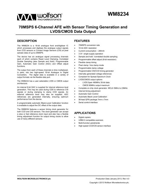
w<strong>WM8234</strong>70MSPS 6-Channel AFE with Sensor Timing Generation andLVDS/CMOS Data OutputDESCRIPTIONFEATURESThe <strong>WM8234</strong> is a 16-bit analogue front end/digitiser ICwhich processes and digitises the analogue output signalsfrom CCD sensors or Contact Image Sensors (CIS) at pixelsample rates of up to 23MSPS.The device has six analogue signal processing channelseach of which contains Reset Level Clamping, CorrelatedDouble Sampling (also Sample and Hold), ProgrammableGain, Automatic Gain Control (AGC) and Offset adjustfunctions.The output from each of these channels is time multiplexed,in pairs, into two high-speed 16-bit Analogue to DigitalConverters. The digital data is available in a variety ofoutput formats via the flexible data port.The <strong>WM8234</strong> has a user selectable LVDS or CMOS outputarchitecture.An internal 8-bit DAC is supplied for internal reference levelgeneration. This may be used during CDS to reference CISsignals or during clamping to clamp CCD signals. Anexternal reference level may also be supplied. ADCreferences are generated internally, ensuring optimumperformance from the device.A programmable automatic Black-Level Calibration functionis available to adjust the DC offset of the output data.70MSPS conversion rate16 bit ADC resolutionCurrent consumption – 280mA3.3V single supply operationSample and hold /correlated double samplingProgrammable offset adjust (8-bit resolution)Flexible clamp timingPixel clamp / line clamp modeProgrammable clamp voltageProgrammable CIS/CCD timing generatorInternally generated voltage referencesCompliant for Spread Spectrum ClockLVDS/CMOS output options LVDS 5pair 490MHz 35-bit data CMOS 90MHz output maximumComplete on chip clock generator. MCLK 5MHz to 23MHzInternal timing adjustmentAutomatic Gain ControlAutomatic Black Level Calibration56-lead QFN package 7mm x 7mmSerial control interfaceThe <strong>WM8234</strong> features a sensor timing clock generator forboth CCD and CIS sensors. The clock generator can accepta slow or fast reference clock input and also has a flexibletiming adjustment function for output timing clocks to allowuse of many different sensors.APPLICATIONS Digital copiers USB2.0 compatible scanners Multi-function peripherals High-speed CCD/CIS sensor interfaceWOLFSON MICROELECTRONICS <strong>plc</strong> Production Data January 2013, <strong>Rev</strong> <strong>4.0</strong>Copyright 2013 <strong>Wolfson</strong> <strong>Microelectronics</strong> <strong>plc</strong>.
<strong>WM8234</strong>BLOCK DIAGRAMProduction DataCLK1CLK2CLK3CLK4CLK5CLK6CLK7CLK8CLK9CLK10CLK11TGSYNCwPD, <strong>Rev</strong> <strong>4.0</strong>, January 20132
<strong>WM8234</strong>Production DatawTABLE OF CONTENTSDESCRIPTION ....................................................................................................... 1FEATURES ............................................................................................................ 1APPLICATIONS ..................................................................................................... 1BLOCK DIAGRAM ................................................................................................ 2TABLE OF CONTENTS ......................................................................................... 3PIN CONFIGURATION .......................................................................................... 5ORDERING INFORMATION .................................................................................. 5PIN DESCRIPTION ................................................................................................ 6ABSOLUTE MAXIMUM RATINGS ........................................................................ 8RECOMMENDED OPERATING CONDITIONS ..................................................... 8ELECTRICAL CHARACTERISTICS ..................................................................... 9GENERAL CHARACTERISTICS ................................................................................... 10INTERNAL POWER ON RESET CIRCUIT .......................................................... 12SIGNAL TIMING REQUIREMENTS .................................................................... 13SERIAL CONTROL INTERFACE .................................................................................. 13DEVICE IDENTIFICATION ............................................................................................ 13REGISTER WRITE ........................................................................................................ 14REGISTER READ-BACK .............................................................................................. 14INPUT VIDEO SAMPLING ............................................................................................ 15SH MODE ................................................................................................................................................ 15CDS MODE .............................................................................................................................................. 15OUTPUT DATA TIMING (CMOS OUTPUT) .................................................................. 16OUTPUT DATA TIMING (LVDS OUTPUT) ................................................................... 16DEVICE DESCRIPTION ...................................................................................... 17INTRODUCTION ........................................................................................................... 17RESET LEVEL CLAMPING (RLC) ................................................................................ 17CDS/NON-CDS PROCESSING..................................................................................... 19OFFSET ADJUST AND PROGRAMMABLE GAIN ........................................................ 20ADC INPUT BLACK LEVEL ADJUST ........................................................................... 20OVERALL SIGNAL FLOW SUMMARY ......................................................................... 21ADC PGA BIAS CURRENT CONTROL ........................................................................ 21PLL DLL SETUP ............................................................................................................ 22OUTPUT DATA FORMAT ............................................................................................. 24LVDS 10-BIT 5PAIR MODE ..................................................................................................................... 24LVDS 16-BIT 5PAIR MODE ..................................................................................................................... 25LVDS 10-BIT 3PAIR MODE ..................................................................................................................... 26LVDS 16-BIT 3PAIR MODE ..................................................................................................................... 27LVDS 12-BIT 4PAIR MODE ..................................................................................................................... 28LVDS DATA OUTPUT ORDER ................................................................................................................ 29CMOS OUTPUT MODE ........................................................................................................................... 30SENSOR TIMING GENERATION ................................................................................. 31TG MASTER MODE OPERATION .......................................................................................................... 32TG SLAVE MODE OPERATION .............................................................................................................. 33TG PULSE AND TRIGGER DATA ........................................................................................................... 34TG PULSE ............................................................................................................................................... 34TRIGGER DATA ...................................................................................................................................... 34CHANNEL ID ........................................................................................................................................... 34TG MASK TIMING ................................................................................................................................... 37TG CYCLE MODE ................................................................................................................................... 38PROGRAMMABLE AUTOMATIC BLACK LEVEL CALIBRATION (BLC) ...................... 39TARGET CODES ..................................................................................................................................... 39PD, <strong>Rev</strong> <strong>4.0</strong>, January 20133
<strong>WM8234</strong>Production DataBLC SCENARIOS OF OPERATION.............................................................................. 40SCENARIO 1 ........................................................................................................................................... 40SCENARIO 2 ........................................................................................................................................... 41SCENARIO 3 ........................................................................................................................................... 41AUTOMATIC GAIN CONTROL (AGC) .......................................................................... 42REGISTER MAP .................................................................................................. 44EXTENDED PAGE REGISTERS................................................................................... 49REGISTER BITS BY ADDRESS ................................................................................... 50APPLICATIONS INFORMATION ...................................................................... 121RECOMMENDED EXTERNAL COMPONENTS ......................................................... 121RECOMMENDED EXTERNAL COMPONENT VALUES ............................................ 122PACKAGE DIMENSIONS .................................................................................. 123IMPORTANT NOTICE ....................................................................................... 124ADDRESS: .................................................................................................................. 124REVISION HISTORY ......................................................................................... 125wPD, <strong>Rev</strong> <strong>4.0</strong>, January 20134
<strong>WM8234</strong>Production DataPIN CONFIGURATIONAGND1AVDD15655IN654IN5IN4IN3IN2IN153 52 51 50 49AVDD2AGND2CLK11CLK10CLK9AGND348 47 46 45 44 43VREF2CVRLC/VBIASVREF3CVREF1CSENSDO12345642 CLK841 CLK740 CLK639 CLK538 CLK437 CLK3SCKSDI78<strong>WM8234</strong>36 CLK235 CLK1LDO2VDD934 TGSYNCLDO2GND 1033LDOV1DDLDO2VOUT 1132LDO1GNDDSLCT2 1231 LDO1VOUTMCLK 1330 MONDSLCT1 1429 HZCTRL15 16 17 18 19 20 21 22 23 24 25 26 2728D5N/OP10D5P/OP9D4N/OP8D4P/OP7DCLKN/OC2DCLKP/OC1DBGNDDBVDDD3N/OP6D3P/OP5D2N/OP4D2P/OP3D1N/OP2D1P/OP1ORDERING INFORMATIONDEVICETEMPERATURERANGEPACKAGEMOISTURESENSITIVITYLEVELPEAK SOLDERINGTEMPERATURE56-lead QFN<strong>WM8234</strong>GEFL/V-40 to 85 o C(7X7x0.85mm)(Pb-free)MSL3260C56-lead QFN<strong>WM8234</strong>GEFL/RV-40 to 85 o C(7X7x0.85mm)(Pb-free, tape and reel)MSL3260CReel quantity = 2,200wPD, <strong>Rev</strong> <strong>4.0</strong>, January 20135
<strong>WM8234</strong>Production DataPIN DESCRIPTIONPIN NAME TYPE DESCRIPTION1 VREF2C Analogue output Mid reference voltage.This pin must be connected to AGND via a decoupling capacitor.2 VRLC Analogue I/O Reference voltage input/output3 VREF3C Analogue output Lower reference voltage.This pin must be connected to AGND via a decoupling capacitor.4 VREF1C Analogue output Upper reference voltage.This pin must be connected to AGND via a decoupling capacitor.5 SEN Digital input Enables the serial interface when high.6 SDO Digital output Serial interface data output7 SCK Digital input Serial interface clock.8 SDI Digital input Serial interface data input9 LDO2VDD Supply Analogue supply10 LDO2GND Supply Analogue ground11 LDO2VOUT Supply LDO outputThis pin must be connected to AGND via a decoupling capacitor.12 DSLCT2 Analogue input Device select 213 MCLK Analogue input Master clock14 DSLCT1 Analogue input Device select 115 D5N/OP[9] LVDS output LVDS Data output 5 – Negative / CMOS output 1116 D5P/OP[8] LVDS output LVDS Data output 5 – Positive / CMOS output 1017 D4N/OP[7] LVDS output LVDS Data output 4 – Negative / CMOS output 918 D4P/OP[6] LVDS output LVDS Data output 4 – Positive / CMOS output 819 DCLKN/OC[2] LVDS output LVDS Clock Output – Negative/ CMOS clock output 220 DCLKP/OC[1] LVDS output LVDS Clock Output – Positive/ CMOS clock output 121 DBGND Supply Analogue ground22 DBVDD Supply Analogue supply23 D3N/OP[5] LVDS output LVDS Data output 3 – Negative / CMOS output 524 D3P/OP[4] LVDS output LVDS Data output 3 – Positive / CMOS output 425 D2N/OP[3] LVDS output LVDS Data output 2 – Negative / CMOS output 326 D2P/OP[2] LVDS output LVDS Data output 2 – Positive / CMOS output 227 D1N/OP[1] LVDS output LVDS Data output 1 – Negative / CMOS output 128 D1P/OP[0] LVDS output LVDS Data output 1 – Positive / CMOS output 029 HZCTRL Digital input Internal use only. Must be connected to AGND.30 MON Analogue output Clock monitor31 LDO1VOUT Supply LDO output.This pin must be connected to AGND via a decoupling capacitor.32 LDO1GND Supply Analogue ground33 LDO1VDD Supply Analogue supply34 TGSYNC Digital input Sensor Timing Sync pulse from host35 CLK1 Digital output Sensor Timing Output 136 CLK2 Digital output Sensor Timing Output 237 CLK3 Digital output Sensor Timing Output 338 CLK4 Digital output Sensor Timing Output 439 CLK5 Digital output Sensor Timing Output 540 CLK6 Digital output Sensor Timing Output 641 CLK7 Digital output Sensor Timing Output 742 CLK8 Digital output Sensor Timing Output 843 AGND3 Supply Analogue ground44 CLK9 Digital output Sensor Timing Output 945 CLK10 Digital output Sensor Timing Output 1046 CLK11 Digital output Sensor Timing Output 11wPD, <strong>Rev</strong> <strong>4.0</strong>, January 20136
<strong>WM8234</strong>Production DataPIN NAME TYPE DESCRIPTION47 AGND2 Supply Analogue ground48 AVDD2 Supply Analogue supply49 IN1 Analogue input Analogue input 150 IN2 Analogue input Analogue input 251 IN3 Analogue input Analogue input 352 IN4 Analogue input Analogue input 453 IN5 Analogue input Analogue input 554 IN6 Analogue input Analogue input 655 AVDD1 Supply Analogue supply56 AGND1 Supply Analogue groundwPD, <strong>Rev</strong> <strong>4.0</strong>, January 20137
<strong>WM8234</strong>Production DataABSOLUTE MAXIMUM RATINGSAbsolute Maximum Ratings are stress ratings only. Permanent damage to the device may be caused by continuously operating ator beyond these limits. Device functional operating limits and guaranteed performance specifications are given under ElectricalCharacteristics at the test conditions specified.ESD Sensitive Device. This device is manufactured on a CMOS process. It is therefore generically susceptibleto damage from excessive static voltages. Proper ESD precautions must be taken during handling and storageof this device.<strong>Wolfson</strong> tests its package types according to IPC/JEDEC J-STD-020 for Moisture Sensitivity to determine acceptable storageconditions prior to surface mount assembly. These levels are:MSL1 = unlimited floor life at
<strong>WM8234</strong>Production DataELECTRICAL CHARACTERISTICSTest ConditionsAVDD = LDOVDD = DBVDD = 3.3V , AGND = LDOGND = DBGND= 0V, T A = 25C, MCLK= 23.3MHz unless otherwise stated.PARAMETER SYMBOL TESTCONDITIONSOverall System Specification (including 10-bit ADC, PGA, Offset and CDS functions)MIN TYP MAX UNITConversion rate per channel 5 23.3 MSPSFull-scale input voltage range(see Note 1)ADCFS=0, Max GainADCFS=0, Min Gain0.122.0Vp-pVp-pADCFS=1, Max GainADCFS=1, Min Gain0.183.0Vp-pVp-pInput signal limits (see Note 2) V IN SF_INP=0 AGND-0.3 AVDD+0.3 VSF_INP=1 AGND AGND+1.2 VInput capacitance C IN Inputs to AGND 10 pFFull-scale transition errorZero-scale transition errorGain = 0dB;AGAIN[4:0] = 02(hex)DGAIN[11:0] = 6AB(hex)Gain = 0dB;AGAIN[4:0] = 02(hex)DGAIN[11:0] = 6AB(hex)20 mV20 mVDifferential non-linearity DNL 10-bit 0.5 LSBIntegral non-linearity (pk-pk/2) INL 10-bit 1 LSBChannel to channel gain matching Min Gain 5 %Output noiseMax Gain 15 %Unity Gain(Unused channels grounded)0.3 LSB rmsChannel to channel crosstalk 10-bit +/-0.5 LSBChannel to channel offsetmatchingProgrammable Gain AmplifierBLC disabled 70 210 mVTotal Resolution (Ga + Gd) GT 12 bitsAnalogue Gain Ga 0.6 + 0.3 * AGAIN[4:0] V/VMax gain, each channel (Ga) Ga MAX AGAIN[4:0] = 1F(hex) 9.9 V/VMin gain, each channel (Ga) Ga MIN AGAIN[4:0] = 0(hex) 0.6 V/VDigital Gain Gd DGAIN[11:0] / 2 11 V/VMax gain, each channel (Gd) Gd MAX DGAIN[11:0] = FFF(hex) 2 V/VMin gain, each channel (Gd) Gd MIN DGAIN[11:0] = 400 (hex) 0.5 V/VMax gain, each channel(Ga + Gd)Min gain, each channel(Ga + Gd)Analogue to Digital ConverterGT MAXGT MINAGAIN[4:0] = 1F(hex)DGAIN[11:0] = FFF(hex)AGAIN[4:0] = 0(hex)DGAIN[11:0] = 400 (hex)19.8 V/V0.3 V/VResolution 16 bitsSpeed 70 MSPSNotes:1. Full-scale input voltage denotes the differential input signal amplitude (V IN -VRLC in non-CDS mode, V IN -RESETlevel in CDS mode) that can be gained to match the ADC full-scale input range.2. Input signal limits are the limits within which each input voltage and VRLC reference must lie.wPD, <strong>Rev</strong> <strong>4.0</strong>, January 20139
<strong>WM8234</strong>Production DataGENERAL CHARACTERISTICSTest ConditionsAVDD = LDOVDD = DBVDD = 3.3V , AGND = LDOGND = DBGND= 0V, T A = 25C, MCLK= 23.3MHz unless otherwise stated.PARAMETER SYMBOL TESTCONDITIONSReferencesMIN TYP MAX UNITUpper reference voltage V REF1C ADCFS=0ADCFS=12.052.25VVLower reference voltage V REF3C ADCFS=0ADCFS=11.251.05VVInput return bias voltage V REF2C 1.2 VDiff. Reference voltage (VREF1C-VREF3C)Output resistance VREF1C,VREF3C, VREF2CV REF1C3CADCFS=0ADCFS=10.81.2VV1 VRLC/Reset-Level Clamp (RLC)RLC switching impedance 50 RLC short-circuit current 2 mARLC output resistance 2 RLC Hi-Z leakage current VRLC = 0 to AVDD 1 ARLCDAC resolution 5 bitsRLCDAC step size V RLCSTEP VRLC_TOP_SEL=0 0.09 V/stepV RLCSTEP VRLC_TOP_SEL=1 0.048 V/stepRLCDAC output voltage atV RLCBOT VRLC_TOP_SEL=0,0.2 Vcode 0(hex)VRLC_VSEL[4:0]=00000V RLCBOT VRLC_TOP_SEL=1,0.11 VVRLC_VSEL[4:0]=00000RLCDAC output voltage atV RLCTOP VRLC_TOP_SEL=0,3.0 Vcode 1F(hex)VRLC_VSEL[4:0]=11111V RLCTOP VRLC_TOP_SEL=1,1.6 VVRLC_VSEL[4:0]=11111VRLC DNL 0.5 LSBVRLC INL 0.5 LSBOffset DAC, Monotonicity GuaranteedResolution 8 bitsDifferential non-linearity DNL 0.5 1 LSBIntegral non-linearity INL 0.5 1 LSBStep size 2.04 mV/stepOutput voltageCode 00(hex)Code FF(hex)-250+250mVmVDIGITAL SPECIFICATIONSDigital InputsHigh level input voltage V IH 0.7 AVDDVLow level input voltage V IL 0.2 AVDDHigh level input current I IH 1 ALow level input current I IL 1 AInput capacitance C I 5 pFVwPD, <strong>Rev</strong> <strong>4.0</strong>, January 201310
<strong>WM8234</strong>Production DataTest ConditionsAVDD = LDOVDD = DBVDD = 3.3V , AGND = LDOGND = DBGND= 0V, T A = 25C, MCLK= 23.3MHz unless otherwise stated.PARAMETER SYMBOL TESTCONDITIONSCMOS OutputsHigh level output voltage V OH I OH = 6mA AVDD– 0.5MIN TYP MAX UNITLow level output voltage V OL I OL = 1mA 0.5 VHigh impedance output current I OZ 1 ATG OutputsHigh level output voltage V OHTG I OH = 1mA AVDD– 0.5Low level output voltage V OLTG I OL = 1mA 0.5 VHigh impedance output current I OZTG Grounded 1 ADigital IO PinsApplied high level input voltage V IH 0.7 AVDDApplied low level input voltage V IL 0.2 AVDDHigh level output voltage V OH I OH = 1mA AVDD– 0.5Low level output voltage V OL I OL = 1mA 0.5 VLow level input current I IL 1 AHigh level input current I IH 1 AInput capacitance C I 5 pFOutput Impedance Ro Io = 1mA 38 ΩHigh impedance output current I OZ 1 ALVDS OutputsDifferential load impedance RL 90 100 110 ΩDifferential steady-state outputvoltage magnitudeChange in the steady-statedifferential output voltagemagnitude between oppositebinary statesSteady-state common-modeoutput voltagePeak-to-peak common-modeoutput|VOD|Δ|VOD|VOC(SS)VOC(PP)RL=100ΩRL=100ΩRL=100Ω280 450 mVVVVVV15 mV1.25 V20 50 mVShort-circuit output current IOS –6 6 mAHigh-impedance state outputcurrentSupply CurrentsTotal supply current full powerdown modeIOZ–10 10 uASF_INP=0, SF_VRLC=0 280 mASF_INP=1, SF_VRLC=1 320 mA1.2 mANotes:1. Full-scale input voltage denotes the differential input signal amplitude (V IN -VRLC in non-CDS mode, V IN -RESETlevel in CDS mode) that can be gained to match the ADC full-scale input range.2. Input signal limits are the limits within which each input voltage and VRLC reference must lie.wPD, <strong>Rev</strong> <strong>4.0</strong>, January 201311
<strong>WM8234</strong>Production DataINTERNAL POWER ON RESET CIRCUITFigure 1 Internal Power On Reset Circuit SchematicThe <strong>WM8234</strong> includes an internal Power-On-Reset Circuit, as shown in Figure 1, which is used resetthe digital logic into a default state after power up. The POR circuit is powered from AVDD andmonitors LDOOUT. It asserts PORB low if AVDD or LDOOUT is below a minimum threshold.Figure 2 Typical Power up Sequence where AVDD is Powered before LDOOUTFigure 2 shows a typical power-up sequence where AVDD is powered up first. When AVDD risesabove the minimum threshold, Vpora, there is enough voltage for the circuit to guarantee PORB isasserted low and the chip is held in reset. In this condition, all writes to the control interface areignored. When LDOOUT rises to Vpord_on, PORB is released high and all registers are in theirdefault state and writes to the control interface may take place. On power down, where AVDD fallsfirst, PORB is asserted low whenever AVDD drops below the minimum threshold Vpora_off.SYMBOL MIN TYP MAX UNITVpora 0.4 0.6 0.8 VVpora_off 0.4 0.6 0.8 VVpord_on 0.5 0.7 0.9 VTable 1 Typical POR Operation (typical values, not tested)wPD, <strong>Rev</strong> <strong>4.0</strong>, January 201312
<strong>WM8234</strong>Production DataINPUT VIDEO SAMPLINGSH MODEFigure 6 Input Video Timing (SH mode)CDS MODEFigure 7 Input Video Timing (CDS mode)Test ConditionsAVDD = LDOVDD = DBVDD = 3.3V , AGND = LDOGND = DBGND= 0V, T A = 25C, MCLK= 23.3MHz unless otherwisestated.PARAMETER SYMBOL TEST CONDITIONS MIN TYP MAX UNITSMCLK cycle period t PER 42.9 nsMCLK high period t MCLKH 14.3 nsMCLK low period t MCLKL 14.3 nsMCLK rising edge to DLL tap 0 t MCLKD 20 nsAperture delay (from RSMP fallingedge)Aperture delay (from VSMP fallingedge)t RSMPD 5 nst VSMPD 5 nsRSMP high period t RSMPH 5 nsVSMP high period t VSMPH 5 8*t PER /60RSMP falling edge to VSMP rising edge tRV 0.5VSMP falling edge to RSMP rising edge tVR 0.5nswPD, <strong>Rev</strong> <strong>4.0</strong>, January 201315
<strong>WM8234</strong>Production DataREGISTERADDRESSR130 (82h)RSMP riseR131 (83h)RSMP fallR132 (84h)VSMP riseR133 (85h)VSMP fallBIT LABEL DEFAULT DESCRIPTION5:0 RSMP_RISE[5:0] 01_1100 RSMP rise edge (0 to 59)5:0 RSMP_FALL[5:0] 10_0110 RSMP fall edge (0 to 59)5:0 VSMP_RISE[5:0] 00_1000 VSMP rise edge (0 to 59)5:0 VSMP_FALL[5:0] 10_1000 VSMP fall edge (0 to 59)OUTPUT DATA TIMING (CMOS OUTPUT)Figure 8 CMOS Output Data TimingTest ConditionsAVDD = LDOVDD = DBVDD = 3.3V , AGND = LDOGND = DBGND= 0V, T A = 25C, MCLK= 23.3MHz unless otherwisestated.PARAMETER SYMBOL TEST CONDITIONS MIN TYP MAX UNITSData output skew t SKOP +/-500 nsOUTPUT DATA TIMING (LVDS OUTPUT)Figure 9 CMOS Output Data TimingTest ConditionsAVDD = LDOVDD = DBVDD = 3.3V , AGND = LDOGND = DBGND= 0V, T A = 25C, MCLK= 23.3MHz unless otherwisestated.PARAMETER SYMBOL TEST CONDITIONS MIN TYP MAX UNITSLVDS output skew t SKLV +/-250 psLVDS output signal rise time t LVTr 1 nsLVDS output signal fall time t LVTf 1 nswPD, <strong>Rev</strong> <strong>4.0</strong>, January 201316
<strong>WM8234</strong>Production DataDEVICE DESCRIPTIONINTRODUCTIONA block diagram of the device showing the signal path is presented on the front page of thisdatasheet.The <strong>WM8234</strong> samples up to six inputs (IN1, IN2, IN3, IN4, IN5, and IN6) simultaneously. The devicethen processes the sampled video signal with respect to the video reset level or aninternally/externally generated reference level using between one and nine processing channels.Each processing channel consists of an Input Sampling block with optional Reset Level Clamping(RLC) and Correlated Double Sampling (CDS), an 8-bit programmable offset DAC and a 12-bitProgrammable Gain Amplifier (PGA).The processing channel outputs are switched, in pairs, alternately by a 2:1 multiplexer to the threeADC inputs.The ADC then converts each resulting analogue signal to a digital word. The digital output from theADC is presented in a variety of possible output formats in LVDS and CMOS format.On-chip control registers determine the configuration of the device, including the offsets and gainsapplied to each channel. These registers are programmable via a serial interface.The device has an automatic Black-Level Calibration function which allows the D.C. offset determinedduring the optically-black pixels at the beginning of the linear sensor to be removed during the imagepixels.The <strong>WM8234</strong> also has an Automatic Gain Control function which automatically adjusts the gain to anappropriate level for a detected input level.The device incorporates a sensor timing generation function which allows CCD and CMOS sensortiming to be controlled directly from the device using internal clock generation and register settings.RESET LEVEL CLAMPING (RLC)To ensure that the signal applied to the <strong>WM8234</strong> lies within the supply voltage range (0V to AVDD)the output signal from a CCD is usually level shifted by coupling through a capacitor, C IN. The RLCcircuit clamps the <strong>WM8234</strong> side of this capacitor to a suitable voltage through a CMOS switch duringthe CCD reset period (pixel clamping) or during the black pixels (line clamping). In order for clampingto produce correct results the input voltage during the clamping must be a constant value.Note that if the ac coupling capacitor (C IN ) is used in non-CDS mode (CDS=0), then to minimise codedrift, line clamping should be used and internal input voltage buffers enabled using the CLPMDregister bit. Alternatively, if the input signal contains a stable reference/reset level then pixel clampingshould be used, and the voltage buffers need not be enabled.The <strong>WM8234</strong> allows the user to control the RLC switch in a variety of ways as illustrated in Figure 10.This figure shows a single channel, however all 6 channels are identical, each with its own clampswitch controlled by the common CLMP signal.The method of control chosen depends upon the characteristics of the input video. The VRLCENregister bit must be set to 1 to enable clamping, otherwise the RLC switch cannot be closed (bydefault VRLCEN=1).Note that unused inputs should be left floating, or grounded through a decoupling capacitor, if resetlevel clamping is used.wPD, <strong>Rev</strong> <strong>4.0</strong>, January 201317
<strong>WM8234</strong>Production DataFigure 10 RLC Clamp Control OptionsWhen an input waveform has a stable reference level on every pixel it may be desirable to clampevery pixel during this period. Setting CLAMP=high means that the RLC switch is closed wheneverthe RSMP is high, as shown in Figure 11..reference("black") levelvideo levelVideo sample taken onfallling edge of VSMPReset/reference sample takenon fallling edge of RSMPRLC switch closedwhen RSMP=1Figure 11 Reset Level Clamp Operation, CDS Operation Shown, non-CDS also PossiblewPD, <strong>Rev</strong> <strong>4.0</strong>, January 201318
<strong>WM8234</strong>Production DataCDS/NON-CDS PROCESSINGFor CCD type input signals, containing a fixed reference/reset level, the signal may be processedusing Correlated Double Sampling (CDS), which will remove pixel-by-pixel common mode noise. WithCDS processing the input waveform is sampled at two different points in time for each pixel, onceduring the reference/reset level and once during the video level. To sample using CDS, register bitCDS must be set to 1 (default = 0). This causes the signal reference to come from the video referencelevel as shown in Figure 12.For input signals that do not contain a reference/reset level (e.g. CIS sensor signals), non-CDSprocessing is used (CDS=0). In this case, the video level is processed with respect to the voltage onpin VRLC/VBIAS. The VRLC/VBIAS voltage is sampled at the same time as input samples the videolevel in this mode. Note that if the ac coupling capacitor (C IN ) is used in non-CDS mode (CDS=0),then to minimise code drift, line clamping should be used and internal input voltage buffers enabledusing the CLPMD register bit. Alternatively, if the input signal contains a stable reference/reset levelthen pixel clamping should be used, and the voltage buffers need not be enabled.C ININ*VS'Video'samplecapacitorCLMPVRLC/VBIASVS'Reference'samplecapacitorVRLC_VSEL[3:0]VRLCENFigure 12 CDS/non-CDS Input ConfigurationwPD, <strong>Rev</strong> <strong>4.0</strong>, January 201319
<strong>WM8234</strong>OVERALL SIGNAL FLOW SUMMARYProduction DataFigure 15 represents the processing of the video signal through the <strong>WM8234</strong>.Figure 15 Overall Signal FlowThe INPUT SAMPLING BLOCK produces an effective input voltage V 1 . For CDS, this is thedifference between the input video level V IN and the input reset level V RESET . For non-CDS this is thedifference between the input video level V IN and the voltage on the VRLC/VBIAS pin, V VRLC , optionallyset via the RLC DAC.The OFFSET DAC BLOCK then adds the amount of fine offset adjustment required to move theblack level of the input signal towards 0V, producing V 2 .The PGA BLOCK then amplifies the white level of the input signal to maximise the ADC range,outputting voltage V 3 .The ADC BLOCK then converts the analogue signal, V 3 , to a 16-bit unsigned digital output, D 1 .The digital output is then inverted, if required, through the OUTPUT INVERT BLOCK to produce D 2.ADC PGA BIAS CURRENT CONTROLThe <strong>WM8234</strong> can be changed the bias current for PGA and ADC comparator as the following step. Itwould be effective for high frequency operation.1. R1C0h=12. R1CBh=11hREGISTERADDRESSR448 (1C0h)User accesscontrol2BIT LABEL DEFAULT DESCRIPTION0 User_KEY2 0 0 = User access2 disabled1 = User access2 enabledREGISTER BIT LABEL DEFAULT DESCRIPTIONADDRESSR459 (1CBh)Comp control1:0 PT_COMP 01 01 = Standard operation11 = High performance operationOther = Inhibit.Notes:1. To change the Comp control, the USER_KEY2 bit must be set to ‘1’.2. If it’s not required to change this register, must be set as default.wPD, <strong>Rev</strong> <strong>4.0</strong>, January 201321
<strong>WM8234</strong>PLL DLL SETUPProduction Data<strong>WM8234</strong> is supporting wide range of input frequency. PLL_EXDIV_SEL[2:0], LVDLGAIN[1:0] andDLGAIN[1:0] must be configured by MCLK clock rate and data output format.Note that after PLL and DLL configuration, the device must be reset as the following step.1. R03[1:0]=11 (PDMD=1, PD=1)2. Delay 1ms3. R03[1:0]=00 (Normal operation)Also, several LVDS operation mode is required to change internal LDO configuration to performLVDS clocking properly. The following register need to set to change the LDO configuration.1. R1B0h=12. R1B4h=12hCMOS 10 bitLVDS 5pair 10bitLVDS 5pair 16bitLVDS 3pair 10bitLVDS 4pair 12bitLVDS 3pair 16bitMax sample rate MCLK Clock rate 23.3 20 18 17.5 15 13.3 12.5 12 10 8.33 7.5 6 5PLL_EXDIV_SEL[2:0] 000 000 000 000 001 001 001 001 00115MHz23.3MHz23.3MHz21MHz10.5MHzLVDLGAIN[1:0]DLGAIN[1:0] 01 10 10 10 10 10 10 10 10LDO settingPLL_EXDIV_SEL[2:0] 001 001 001 001 001 001 001 010 010 010 010 011 011LVDLGAIN[1:0] 00 00 01 01 01 01 01 01 01 01 01 10 10DLGAIN[1:0] 01 01 01 01 01 10 10 10 10 10 10 10 10LDO setting 12h 12hPLL_EXDIV_SEL[2:0] 001 001 001 001 001 001 001 001 001 001 010 010 010LVDLGAIN[1:0] 00 00 00 00 00 01 01 01 01 01 01 01 01DLGAIN[1:0] 01 01 01 01 01 10 10 10 10 10 10 10 10LDO setting 12h 12h 12h 12h 12hPLL_EXDIV_SEL[2:0] 001 001 001 001 001 001 001 001 001 010 010 010LVDLGAIN[1:0] 00 00 00 00 01 01 01 01 01 01 01 01DLGAIN[1:0] 01 01 01 01 10 10 10 10 10 10 10 10LDO setting 12h 12h 12h 12hPLL_EXDIV_SEL[2:0] 001 001 001 001 001LVDLGAIN[1:0] 00 00 00 01 01DLGAIN[1:0] 10 10 10 10 10LDO setting 12h 12h 12hREGISTERADDRESSR28 (1Ch)PLL dividercontrol 1BIT LABEL DEFAULT DESCRIPTION6 PLL_EXDIV_SEL5 PLL_EXDIV_SEL0 Select EX DIV ratio.Need to set according to input frequency. See details in PLLDLL setup000 = 1001 = 2010 = 4011 = 8100 = 16101 to 111 = reserved.0 Select EX DIV ratio.Need to set according to input frequency. See details in PLLDLL setup000 = 1001 = 2010 = 4011 = 8100 = 16101 to 111 = reserved.wPD, <strong>Rev</strong> <strong>4.0</strong>, January 201322
<strong>WM8234</strong>REGISTERADDRESSBIT LABEL DEFAULT DESCRIPTION4 PLL_EXDIV_SEL1 Select EX DIV ratio.Need to set according to input frequency. See details in PLLDLL setup000 = 1001 = 2010 = 4011 = 8100 = 16101 to 111 = reserved.Production DataREGISTERADDRESSR128 (80h)DLL config 1BIT LABEL DEFAULT DESCRIPTION5 DLGAIN 1 gain control of DLL delay lineNeed to set according to input frequency. See details in PLLDLL setup4 DLGAIN 0 gain control of DLL delay lineNeed to set according to input frequency. See details in PLLDLL setupREGISTERADDRESSR129 (81h)DLL config 2BIT LABEL DEFAULT DESCRIPTION5 LVDLGAIN 0 gain control of LVDS DLL delay lineNeed to set according to input frequency. See details in PLLDLL setup4 LVDLGAIN 1 gain control of LVDS DLL delay lineNeed to set according to input frequency. See details in PLLDLL setupREGISTERADDRESSR432 (1B0h)User accesscontrolBIT LABEL DEFAULT DESCRIPTION0 USER_KEY 0 0 = User access disabled1 = User access enabledREGISTERADDRESSR436 (1B4h)LDO2 controlBIT LABEL DEFAULT DESCRIPTION4:0 LDO2 VSEL 1_0000 1_0000 = 1.8V1_0010 = 2.0VNotes:1. To change the LDO2 control, the USER_KEY bit must be set to ‘1’.2. If it’s not required to change this register, it must be set as default.wPD, <strong>Rev</strong> <strong>4.0</strong>, January 201323
<strong>WM8234</strong>Production DataOUTPUT DATA FORMATThe output from the <strong>WM8234</strong> can be presented in several different formats under control ofthe CMOSMODE and the LVDSMODE register. Depending on the output modes, maximumMCLK rate is different as sown in Table 4.MODES DESCRIPTION OUTPUTDATA RATEMAXIMUMMCLK RATE1 LVDS 10-bit 5pair MCLK x21 23.3MSPS2 LVDS 16-bit 5pair MCLK x31.5 15.5MSPS3 LVDS 10-bit 3pair MCLK x21 21.0MSPS4 LVDS 16-bit 3pair MCLK x42 10.5MSPS5 LVDS 12-bit 4pair MCLK x21 21.0MSPS6 CMOS 10-bit MCLK x9 10MSPSTable 4 Output Format and Data RateLVDS 10-BIT 5PAIR MODEAD5 S0 S1 S2 IN1[0] IN1[1] IN1[2] IN1[3]D4 IN1[4] IN1[5] IN1[6] IN1[7] IN1[8] IN1[9] S3D3 S4 IN2[0] IN2[1] IN2[2] IN2[3] IN2[4] IN2[5]D2 IN2[6] IN2[7] IN2[8] IN2[9] IN3[0] IN3[1] IN3[2]D1 IN3[3] IN3[4] IN3[5] IN3[6] IN3[7] IN3[8] IN3[9]DCLK H H L L L H HBD5 S0 S1 S2 IN4[0] IN4[1] IN4[2] IN4[3]D4 IN4[4] IN4[5] IN4[6] IN4[7] IN4[8] IN4[9] S3D3 S4 IN5[0] IN5[1] IN5[2] IN5[3] IN5[4] IN5[5]D2 IN5[6] IN5[7] IN5[8] IN5[9] IN6[0] IN6[1] IN6[2]D1 IN6[3] IN6[4] IN6[5] IN6[6] IN6[7] IN6[8] IN6[9]DCLK H H L L L H HTable 5 10-bit 5pair LVDS Output FormatwPD, <strong>Rev</strong> <strong>4.0</strong>, January 201324
<strong>WM8234</strong>Production DataLVDS 16-BIT 5PAIR MODEAD5 S0 S1 S2 IN1[0] IN1[1] IN1[2] IN1[3]D4 IN1[4] IN1[5] IN1[6] IN1[7] IN1[8] IN1[9] IN1[10]D3 IN1[11] IN1[12] IN1[13] IN1[14] IN1[15] IN2[0] IN2[1]D2 IN2[2] IN2[3] IN2[4] IN2[5] IN2[6] IN2[7] IN2[8]D1 IN2[9] IN2[10] IN2[11] IN2[12] IN2[13] IN2[14] IN2[15]DCLK H H L L L H HBD5 S0 S1 S2 IN[0] IN3[1] IN3[2] IN3[3]D4 IN3[4] IN3[5] IN3[6] IN3[7] IN3[8] IN3[9] IN3[10]D3 IN3[11] IN3[12] IN3[13] IN3[14] IN3[15] IN4[0] IN4[1]D2 IN4[2] IN4[3] IN4[4] IN4[5] IN4[6] IN4[7] IN4[8]D1 IN4[9] IN4[10] IN4[11] IN4[12] IN4[13] IN4[14] IN4[15]DCLK H H L L L H HCD5 S0 S1 S2 INP5[0] INP5[1] INP5[2] INP5[3]D4 INP5[4] INP5[5] INP5[6] INP5[7] INP5[8] INP5[9] INP5[10]D3 INP5[11] INP5[12] INP5[13] INP5[14] INP5[15] INP6[0] INP6[1]D2 INP6[2] INP6[3] INP6[4] INP6[5] INP6[6] INP6[7] INP6[8]D1 INP6[9] INP6[10] INP611] INP6[12] INP6[13] INP6[14] INP6[15]DCLK H H L L L H HTable 6 16-bit 5pair LVDS Output FormatwPD, <strong>Rev</strong> <strong>4.0</strong>, January 201325
<strong>WM8234</strong>LVDS 10-BIT 3PAIR MODEProduction DataIN1IN2IN3IN4IN5IN6IN1 IN2 IN3IN4 IN5 IN6H H L L L H H H H L L L H H H H L L L H HAD3 S0 IN1[0] IN1[1] IN1[2] IN1[3] IN1[4] IN1[5]D2 IN1[6] IN1[7] IN1[8] IN1[9] IN2[0] IN2[1] IN2[2]D1 IN2[3] IN2[4] IN2[5] IN2[6] IN2[7] IN2[8] IN2[9]DCLK H H L L L H HBD3 S0 IN3[0] IN3[1] IN3[2] IN3[3] IN3[4] IN3[5]D2 IN3[6] IN3[7] IN3[8] IN3[9] IN4[0] IN4[1] IN4[2]D1 IN4[3] IN4[4] IN4[5] IN4[6] IN4[7] IN4[8] IN4[9]DCLK H H L L L H HCD3 S0 IN5[0] IN5[1] IN5[2] IN5[3] IN5[4] IN5[5]D2 IN5[6] IN5[7] IN5[8] IN5[9] IN6[0] IN6[1] IN6[2]D1 IN6[3] IN6[4] IN6[5] IN6[6] IN6[7] IN6[8] IN6[9]DCLK H H L L L H HTable 7 10-bit 3pair LVDS Output FormatwPD, <strong>Rev</strong> <strong>4.0</strong>, January 201326
<strong>WM8234</strong>Production DataLVDS 16-BIT 3PAIR MODEAD3 S0 S1 S2 IN1[0] IN1[1] IN1[2] IN1[3]D2 IN1[4] IN1[5] IN1[6] IN1[7] IN1[8] IN1[9] IN1[10]D1 IN1[11] IN1[12] IN1[13] IN1[14] IN1[15] S3 S4DCLK H H L L L H HBD3 S0 S1 S2 IN2[0] IN2[1] IN2[2] IN2[3]D2 IN2[4] IN2[5] IN2[6] IN2[7] IN2[8] IN2[9] IN2[10]D1 IN2[11] IN2[12] IN2[13] IN2[14] IN2[15] S3 S4DCLK H H L L L H HFD3 S0 S1 S2 IN6[0] IN6[1] IN6[2] IN6[3]D2 IN6[4] IN6[5] IN6[6] IN6[7] IN6[8] IN6[9] IN6[10]D1 IN6[11] IN6[12] IN6[13] IN6[14] IN6[15] S3 S4DCLK H H L L L H HTable 8 16-bit 3pair LVDS Output FormatNote:A: IN1, B:IN2, C:IN3, D:IN4. E:IN5, F:IN6wPD, <strong>Rev</strong> <strong>4.0</strong>, January 201327
<strong>WM8234</strong>Production DataLVDS 12-BIT 4PAIR MODEAD4 S0 IN1[0] IN1[1] IN1[2] IN1[3] IN1[4] IN1[5]D3 IN1[6] IN1[7] IN1[8] IN1[9] IN1[10] IN1[11] S1D2 S2 S3 IN2[0] IN2[1] IN2[2] IN2[3] IN2[4]D1 IN2[5] IN2[6] IN2[7] IN2[8] IN2[9] IN2[10] IN2[11]DCLK H H L L L H HBD4 S0 IN3[0] IN3[1] IN3[2] IN3[3] IN3[4] IN3[5]D3 IN3[6] IN3[7] IN3[8] IN3[9] IN3[10] IN3[11] S1D2 S2 S3 IN4[0] IN4[1] IN4[2] IN4[3] IN4[4]D1 IN4[5] IN4[6] IN4[7] IN4[8] IN4[9] IN4[10] IN4[11]DCLK H H L L L H HCD4 S0 IN5[0] IN5[1] IN5[2] IN5[3] IN5[4] IN5[5]D3 IN5[6] IN5[7] IN5[8] IN5[9] IN5[10] IN5[11] S1D2 S2 S3 IN6[0] IN6[1] IN6[2] IN6[3] IN6[4]D1 IN6[5] IN6[6] IN6[7] IN6[8] IN6[9] IN6[10] IN6[11]DCLK H H L L L H HTable 9 12-bit 4pair LVDS Output FormatwPD, <strong>Rev</strong> <strong>4.0</strong>, January 201328
<strong>WM8234</strong>Production DataLVDS DATA OUTPUT ORDERThe <strong>WM8234</strong> can be presented 2 types of LVDS data output order, Ascending order modeand Descending order mode as the following.Ascending Order ModeDecending Order Mode10bit 5pair mode10bit 5pair modeD5 S0 S1 S2 IN1[0] IN1[1] IN1[2] IN1[3] D5 S4 S3 S2 IN1[9] IN1[8] IN1[7] IN1[6]D4 IN1[4] IN1[5] IN1[6] IN1[7] IN1[8] IN1[9] S3 D4 IN1[5] IN1[4] IN1[3] IN1[2] IN1[1] IN1[0] S1D3 S4 IN2[0] IN2[1] IN2[2] IN2[3] IN2[4] IN2[5] D3 S0 IN2[9] IN2[8] IN2[7] IN2[6] IN2[5] IN2[4]D2 IN2[6] IN2[7] IN2[8] IN2[9] IN3[0] IN3[1] IN3[2] D2 IN2[3] IN2[2] IN2[1] IN2[0] IN3[9] IN3[8] IN3[7]D1 IN3[3] IN3[4] IN3[5] IN3[6] IN3[7] IN3[8] IN3[9] D1 IN3[6] IN3[5] IN3[4] IN3[3] IN3[2] IN3[1] IN3[0]DCLK H H L L L H H DCLK H H L L L H H16bit 5pair mode16bit 5pair modeD5 S0 S1 S2 IN1[0] IN1[1] IN1[2] IN1[3] D5 S2 S1 S0 IN1[15] IN1[14]IN1[13]IN1[12]D4 IN1[4] IN1[5] IN1[6] IN1[7] IN1[8] IN1[9] IN1[10] D4 IN1[11]IN1[10] IN1[9] IN1[8] IN1[7] IN1[6] IN1[5]D3 IN1[11]IN1[12]IN1[13]IN1[14]IN1[15] IN2[0] IN2[1] D3 IN1[4] IN1[3] IN1[2] IN1[1] IN1[0] IN2[15] IN2[14]D2 IN2[2] IN2[3] IN2[4] IN2[5] IN2[6] IN2[7] IN2[8] D2 IN2[13]IN2[12]IN2[11]IN2[10] IN2[9] IN2[8] IN2[7]D1 IN2[9] IN2[10] IN211]IN2[12]IN2[13]IN2[14]IN2[15] D1 IN2[6] IN2[5] IN2[4] IN2[3] IN2[2] IN2[1] IN2[0]DCLK H H L L L H H DCLK H H L L L H H10bit 3pair mode10bit 3pair modeD3 S0 IN1[0] IN1[1] IN1[2] IN1[3] IN1[4] IN1[5] D3 S0 IN1[9] IN1[8] IN1[7] IN1[6] IN1[5] IN1[4]D2 IN1[6] IN1[7] IN1[8] IN1[9] IN2[0] IN2[1] IN2[2] D2 IN1[3] IN1[2] IN1[1] IN1[0] IN2[9] IN2[8] IN2[7]D1 IN2[3] IN2[4] IN2[5] IN2[6] IN2[7] IN2[8] IN2[9] D1 IN2[6] IN2[5] IN2[4] IN2[3] IN2[2] IN2[1] IN2[0]DCLK H H L L L H H DCLK H H L L L H H16bit 3pair mode16bit 3pair modeD3 S0 S1 S2 IN1[0] IN1[1] IN1[2] IN1[3] D3 S4 S3 S2 IN1[15] IN1[14]IN1[13]IN1[12]D2 IN1[4] IN1[5] IN1[6] IN1[7] IN1[8] IN1[9] IN1[10] D2 IN1[11]IN1[10] IN1[9] IN1[8] IN1[7] IN1[6] IN1[5]D1 IN111]IN1[12]IN1[13]IN1[14]IN1[15] S3 S4 D1 IN1[4] IN1[3] IN1[2] IN1[1] IN1[0] S1 S0DCLK H H L L L H H DCLK H H L L L H H12bit 4pair mode12bit 4pair modeD4 S0 IN1[0] IN1[1] IN1[2] IN1[3] IN1[4] IN1[5] D4 S3 IN1[11] IN1[10] IN1[9] IN1[8] IN1[7] IN1[6]D3 IN1[6] IN1[7] IN1[8] IN1[9] IN1[10]IN1[11] S1 D3 IN1[5] IN1[4] IN1[3] IN1[2] IN1[1] IN1[0] S2D2 S2 S3 IN2[0] IN2[1] IN2[2] IN2[3] IN2[4] D2 S1 S0 IN2[11] IN2[10] IN2[9] IN2[8] IN2[7]D1 IN2[5] IN2[6] IN2[7] IN2[8] IN2[9] IN2[10] IN211] D1 IN2[6] IN2[5] IN2[4] IN2[3] IN2[2] IN2[1] IN2[0]DCLK H H L L L H H DCLK H H L L L H HREGISTERADDRESSR7 (07h)outputcontrolBIT LABEL DEFAULT DESCRIPTION3 LVDSORDER 0 control LVDS data output order0 = descending order1 = ascending orderwPD, <strong>Rev</strong> <strong>4.0</strong>, January 201329
<strong>WM8234</strong>Production DataCMOS OUTPUT MODEAOP9 IN1[9] IN2[9] IN3[9] IN4[9] IN5[9] IN6[9]OP8 IN1[8] IN2[8] IN3[8] IN4[8] IN5[8] IN6[8]OP7 IN1[7] IN2[7] IN3[7] IN4[7] IN5[7] IN6[7]OP6 IN1[6] IN2[6] IN3[6] IN4[6] IN5[6] IN6[6]OP5 IN1[5] IN2[5] IN3[5] IN4[5] IN5[5] IN6[5]OP4 IN1[4] IN2[4] IN3[4] IN4[4] IN5[4] IN6[4]OP3 IN1[3] IN2[3] IN3[3] IN4[3] IN5[3] IN6[3]OP2 IN1[2] IN2[2] IN3[2] IN4[2] IN5[2] IN6[2]OP1 IN1[1] IN2[1] IN3[1] IN4[1] IN5[1] IN6[1]OP0 IN1[0] IN2[0] IN3[0] IN4[0] IN5[0] IN6[0]Table 10 10-bit CMOS Output FormatwPD, <strong>Rev</strong> <strong>4.0</strong>, January 201330
<strong>WM8234</strong>Production DataSENSOR TIMING GENERATIONThe <strong>WM8234</strong> provides two types of clock internally. C_CK* are high speed clocks, theseclocks can set the clock phase by using fine pitch phase control. P_CK* are pixel rate signalswhich is selected by PO0 to PO7. The <strong>WM8234</strong> has eleven sensor TG outputs pins. CLK1 isfor clock type use only. CLK2, CLK3, CLK4, CLK5 and CLK6 are selectable high speed typesignal or pulse type signal. CLK7, CLK8, CLK9, CLK10 and CLK11 are pulse type use only.Figure 16 TG Output TimingwPD, <strong>Rev</strong> <strong>4.0</strong>, January 201331
<strong>WM8234</strong>Production DataTest ConditionsAVDD = LDOVDD = DBVDD = 3.3V , AGND = LDOGND = DBGND= 0V, T A = 25C, MCLK= 23.3MHz unless otherwisestated.PARAMETER SYMBOL TEST CONDITIONS MIN TYP MAX UNITSMCLK cycle period t PER 28.6 nsMCLK rising edge to DLL tap 0 t MCLKD 20 nsREGISTERADDRESSR176 (B0h)– R177 (B1h)R135 (81h)– R146 (92h)BIT LABEL DEFAULT DESCRIPTION5:0 DEL_PCK*[1:0] 00 control delay for pulse output00 = 0nsec, 01 = 1nsec, 10 = 2nsec, 11 = 3nsec5:0 CLK*_RISE[5:0] CLK* rise edge (0 to 59)5:0 CLK*_FALL[5:0] CLK* fall edge (0 to 59)TG MASTER MODE OPERATIONIn muster mode, line length is defined by LLENGTH register.Figure 17 Master Mode Pixel Counter and Line Start TimingPARAMETER SYMBOL TEST CONDITIONS MIN TYP MAX UNITSData trigger timing delay t TRIGD 10 clockTG pulse output timing delay t PCKD 2 clockwPD, <strong>Rev</strong> <strong>4.0</strong>, January 201332
<strong>WM8234</strong>Production DataTG SLAVE MODE OPERATIONIn slave mode, line length depends on TGSYNC input. The pixel counter is reset by TGSYNC input.Figure 18 Slave Mode Pixel Counter and Line Start TimingPARAMETER SYMBOL TEST CONDITIONS MIN TYP MAX UNITSMCLK cycle period tPER 28.6 nsTGSYNC Setup time t SCKSY tPER/2 nsPixel counter start timingt COUNTD 2 clock(only for slave mode)TGSYNC pulse widtht SYH 1 clock(only for slave mode)Data trigger timing delay t TRIGD 10 clockTG pulse output timing delay t PCKD 2 clockREGISTER BIT LABEL DEFAULT DESCRIPTIONADDRESSR160 (A0h) 7:4 OFFSET[3:0] 0000 offset count (only for slave mode)2 POLSYNC 0 polarity of Sync signal0 = POSITIVE EDGE, 1 = NEGATIVE EDGE1 TGMD 0 TG operation mode0 = SLAVE, 1 = MASTER0 TG_EN 0 TG enable0 = DISABLE, 1 = ENABLER161 (A1h) 7:0 LLENGTH[7:0] 0000_0000 the number of pixels in 1line (only for master mode)R162 (A2h) 6:0 LLENGTH[6:0] 000_0000 the number of pixels in 1line (only for master mode)wPD, <strong>Rev</strong> <strong>4.0</strong>, January 201333
<strong>WM8234</strong>TG PULSE AND TRIGGER DATAProduction DataFigure 19 TG Pulse Toggle Setting and Data Trigger TimingTG PULSE<strong>WM8234</strong> can be generated 8 TG pulse internally (PO0 – PO7). These pulses are generatedby toggle point setting register (TP*) and polarity setting register (POL*_PO*). <strong>WM8234</strong>provided up to 32 toggle point by using TP0 to TP31. PO0-PO7 signals can be assigned toCLK2-CLK8 by SEL_PCK* and SEL_CLK* register.TRIGGER DATA<strong>WM8234</strong> can implement trigger data in LVDS flag data (S0, S1, S2, S3 and S4). This can beselected from two methods. One is FLAGPIX register, this can be set one pixel by each line.The other is to apply PO* pulse. Figure 19 shows the trigger data implementation timing.CHANNEL IDAlso <strong>WM8234</strong> can implement channel identification data instead of trigger data. Table 9shows the matrix of input channel and channel ID.ID[2] ID[1] ID[0]IN1 0 0 1IN2 0 1 0IN3 0 1 1IN4 1 0 0IN5 1 0 1IN6 1 1 0Table 11 Channel IDChannel ID can be assigned to flag data (S0, S1, S2, S3 or S4). The following is the exampleof channel ID assignment.Example)Assigned channel ID to flag data as ID[2] =S1, ID[1]=S2, ID[0]=S3.If output data is as follows, channel ID will be IN1. (i.e. ID[2]=S1=0, ID[1]=S2=0, ID[0]=S3=1)AD5 S0 S1 S2 IN1[0] IN1[1] IN1[2] IN1[3]D4 IN1[4] IN1[5] IN1[6] IN1[7] IN1[8] IN1[9] S3D3 S4 IN2[0] IN2[1] IN2[2] IN2[3] IN2[4] IN2[5]D2 IN2[6] IN2[7] IN2[8] IN2[9] IN3[0] IN3[1] IN3[2]D1 IN3[3] IN3[4] IN3[5] IN3[6] IN3[7] IN3[8] IN3[9]DCLK H H L L L H HwPD, <strong>Rev</strong> <strong>4.0</strong>, January 201334
<strong>WM8234</strong>Production DataChannel ID Setting LimitationThere are some notices to assign channel ID. It’s depending on LVDS output format. (refer toOUTPUT DATA FORMAT)1. 10-bit 5pair mode LVDS outputIn this mode, channel ID will be IN1, IN4 only.Case-1 ID indicate IN1AD5 S0 S1 S2 IN1[0] IN1[1] IN1[2] IN1[3]D4 IN1[4] IN1[5] IN1[6] IN1[7] IN1[8] IN1[9] S3D3 S4 IN2[0] IN2[1] IN2[2] IN2[3] IN2[4] IN2[5]D2 IN2[6] IN2[7] IN2[8] IN2[9] IN3[0] IN3[1] IN3[2]D1 IN3[3] IN3[4] IN3[5] IN3[6] IN3[7] IN3[8] IN3[9]DCLK H H L L L H HCase-2 ID indicate IN4BD5 S0 S1 S2 IN4[0] IN4[1] IN4[2] IN4[3]D4 IN4[4] IN4[5] IN4[6] IN4[7] IN4[8] IN4[9] S3D3 S4 IN5[0] IN5[1] IN5[2] IN5[3] IN5[4] IN5[5]D2 IN5[6] IN5[7] IN5[8] IN5[9] IN6[0] IN6[1] IN6[2]D1 IN6[3] IN6[4] IN6[5] IN6[6] IN6[7] IN6[8] IN6[9]DCLK H H L L L H H2. 16-bit 5pair mode LVDS outputThis mode has only three data flags as S0, S1 and S2. Therefore it cannot assign all channelID to data flags.AD5 S0 S1 S2 IN1[0] IN1[1] IN1[2] IN1[3]D4 IN1[4] IN1[5] IN1[6] IN1[7] IN1[8] IN1[9] IN1[10]D3 IN1[11] IN1[12] IN1[13] IN1[14] IN1[15] IN2[0] IN2[1]D2 IN2[2] IN2[3] IN2[4] IN2[5] IN2[6] IN2[7] IN2[8]D1 IN2[9] IN2[10] IN2[11] IN2[12] IN2[13] IN2[14] IN2[15]DCLK H H L L L H HPARAMETER SYMBOL TEST CONDITIONS MIN TYP MAX UNITSData trigger timing delay t TRIGD 10 clockREGISTERADDRESSR171 (ABh)- R175 (AFh)R208 (D0h)- R270 (10Eh)BIT LABEL DEFAULT DESCRIPTIONSEL_PCK* 000 pulse mapping control for CLK*000 = PO1, 001 = PO2, 010 = PO3, 011 = PO4100 = PO5, 101 = PO6, 110 = PO7, 111 = PO8SEL_CLK* 0 mapping control0 = output clock, 1 = output pulse7 EN_TP* 0 enable toggle point0 = disable and subsequent toggle point1 = enable toggle point6:0 TP* pixel count of toggle pointwPD, <strong>Rev</strong> <strong>4.0</strong>, January 201335
<strong>WM8234</strong>Production DataREGISTER BIT LABEL DEFAULT DESCRIPTIONADDRESSR271 (10Fh)POL*_PO*polarity of PO* pulse at TP*- R310 (136h)R163 (A3h) 7:0 FLAGPIX[7:0] 0000_0000 flag pixelR164 (A4h) 6:0 FLAGPIX[6:0] 000_0000 flag pixelR180 (B4h) 3:0 SEL_FLAG[3:0] 0000 select signal to be output as datatrig0xxx = flagpix, 1000 = PO0, 1001 = PO1, 1010 = PO2,1011 = PO3, 1100 = PO4, 1101 = PO5, 1110 = PO61111 = PO7R10 (0Ah) 7:4 FLAG_S1[3:0] 0001 output dataflag as S1(valid only LVDS mode)0000 = always low, 0001 = start flag0010 = reserved, 0011 = reserved, 0100 = reserved0101 = channel ID[0], 0110 = channel ID[1],0111 = channel ID[2], 1000 = reserved1001 = reserved, 1010 = reserved, 1011 = reserved,1100 = reserved, 1101 = reserved, 1110 = reserved1111 = always high3:0 FLAG_S0[3:0] 0000 output dataflag as S0(valid only LVDS mode)0000 = always low, 0001 = start flag0010 = reserved, 0011 = reserved, 0100 = reserved0101 = channel ID[0], 0110 = channel ID[1],0111 = channel ID[2], 1000 = reserved1001 = reserved, 1010 = reserved, 1011 = reserved,1100 = reserved, 1101 = reserved, 1110 = reserved1111 = always highR11 (0Bh) 7:4 FLAG_S3[3:0] 0001 output dataflag as S3(valid only LVDS mode)0000 = always low, 0001 = start flag0010 = reserved, 0011 = reserved, 0100 = reserved0101 = channel ID[0], 0110 = channel ID[1],0111 = channel ID[2], 1000 = reserved1001 = reserved, 1010 = reserved, 1011 = reserved,1100 = reserved, 1101 = reserved, 1110 = reserved1111 = always high3:0 FLAG_S2[3:0] 0000 output dataflag as S2(valid only LVDS mode)0000 = always low, 0001 = start flag0010 = reserved, 0011 = reserved, 0100 = reserved0101 = channel ID[0], 0110 = channel ID[1],0111 = channel ID[2], 1000 = reserved1001 = reserved, 1010 = reserved, 1011 = reserved,1100 = reserved, 1101 = reserved, 1110 = reserved1111 = always highR12 (0Ch) 3:0 FLAG_S4[3:0] 0000 output dataflag as S4(valid only LVDS mode)0000 = always low, 0001 = start flag0010 = reserved, 0011 = reserved, 0100 = reserved0101 = channel ID[0], 0110 = channel ID[1],0111 = channel ID[2], 1000 = reserved1001 = reserved, 1010 = reserved, 1011 = reserved,1100 = reserved, 1101 = reserved, 1110 = reserved1111 = always highwPD, <strong>Rev</strong> <strong>4.0</strong>, January 201336
<strong>WM8234</strong>Production DataTG MASK TIMING<strong>WM8234</strong> has TG clock mask function. M1, M2 and M3 pulse specifies the mask period, T1and T2 pulses are used for changing the signal polarity during the mask period. C_CK1 andC_CK2 are applied M pulse only, they cannot apply T pulse. C_CK3 and C_CK4 are appliedM2 and T2, C_CK5 and C_CK6 are applied M1 and T1.The mask timing is synchronized withTGCKO rise edge.Figure 20 TG Mask TimingTG CLOCKC_CK1C_CK2C_CK3C_CK4C_CK5C_CK6APPLIED“M” PULSEM3M1M2APPLIED“T” PULSEnoneT1T2REGISTER BIT LABEL DEFAULT DESCRIPTIONADDRESSR195 (C3h) 7:0 M1_RISE[7:0] 0000_0000 M1 pulse rise count (mask start)R196 (C4h) 6:0 M1_RISE[6:0] 000_0000 M1 pulse rise count (mask start)R197 (C5h) 7:0 M1_FALL[7:0] 0000_0000 M1 pulse fall count (mask end)R198 (C6h) 6:0 M1_FALL[6:0] 000_0000 M1 pulse fall count (mask end)R199 (C7h) 7:0 M2_RISE[7:0] 0000_0000 M2 pulse rise count (mask start)R200 (C8h) 6:0 M2_RISE[6:0] 000_0000 M2 pulse rise count (mask start)R201 (C9h) 7:0 M2_FALL[7:0] 0000_0000 M2 pulse fall count (mask end)R202 (CAh) 6:0 M2_FALL[6:0] 000_0000 M2 pulse fall count (mask end)R203 (CBh) 7:0 M3_RISE[7:0] 0000_0000 M3 pulse rise count (mask start)R204 (CCh) 6:0 M3_RISE[6:0] 000_0000 M3 pulse rise count (mask start)R205 (CDh) 7:0 M3_FALL[7:0] 0000_0000 M3 pulse fall count (mask end)R206 (CEh) 6:0 M3_FALL[6:0] 000_0000 M3 pulse fall count (mask end)R271 (010Fh) 7:0 POL*_T1 1111_1111 polarity of T1 pulse at TP*– R278 (116h) 7:0 POL*_T2 1111_1111 polarity of T2 pulse at TP*wPD, <strong>Rev</strong> <strong>4.0</strong>, January 201337
<strong>WM8234</strong>Production DataPROGRAMMABLE AUTOMATIC BLACK LEVEL CALIBRATION (BLC)The Programmable Automatic Black-Level Calibration (BLC) function is to adjust the D.C. offset of theoutput data such that the digital output code for black pixels is calibrated to a target black level value.The D.C. offset is determined during the optically-black pixels at the beginning of the linear sensor,and removed during the image-pixels as shown in Figure 22.Black Pixel PeriodImage Pixel PeriodDetermine BlackLevel OffsetRemove Black Level Offsetfrom Image PixelsFigure 22 Linear Sensor ModelThe automatic black level calibration operates assuming 12 bits ADC resolution. Adjustments tocalculations must be made for different ADC resolutions.The black level calibration process occurs in two stages as shown in Figure 23 below:Coarse Adjust Calibration: This is a mixed signal loop which removes the coarse offset byadjusting the offset DAC.Fine Adjust Calibration: This is a digital loop which removes the remaining offset withbetter noise tolerance, utilising ADC over-range to improve the dynamic range of thesystem.Input Black Level V1PGAADCAdjustedADC OutputOffsetDACCoarse AdjustCalibrationMixedSignalLOOPDigitsFine AdjustCalibrationDigitalLOOPDigitsTARGET BLFigure 23 BLC Top-Level CircuitryTARGET CODESThe user must specify a target black level for each channel through the registers TARGETINP*. If,during the black-pixel period, the average ADC output code was, for example, 100 and the userspecified the target black level code to be 10, the BLC circuitry would determine 90 codes should besubtracted from the ADC output. These 90 codes will then be subtracted from every image-pixel codeoutput from the ADC.Note – changing the PGA gain affects the black-level through the device; the gain should thereforenot be changed during a BLC procedure. If the PGA gain changes, then the BLC routine should bere-run.wPD, <strong>Rev</strong> <strong>4.0</strong>, January 201339
<strong>WM8234</strong>Production DataThe automatic black level calibration feature operates with the assumption of a 12-bit ADC resolution.The register settings for Target Codes (TARGETINP*) should be set differently depending on theADC resolution being used. As TARGETINP* is an 8-bit register, the 4 MSBs of a data output codecannot be changed.16-bit ADC ResolutionFor 16-bit resolution the target code entered into TARGETINP* will ignore the 4 MSBs and 4 LSBs ofthe 16-bit data output. For example if the desired code out is 0000111111110001, the value enteredinto TARGETINP* would be 11111111.10-bit ADC ResolutionBLC SCENARIOS OF OPERATIONFor 10-bit resolution the 4 MSBs of the 10bit data output code will be ignored. The 2 LSBs of thetarget code should be set to ‘00’. For example if the desired code out is 0000111111, the valueentered into TARGETINP* would be 11111100.The BLC can be used in various ways to suit the application, for example calibration can be doneonce per page or once per line. Three potential scenarios of operation are suggested below.Note: The registers FRAME_START and SEQ_START when set high by the user will automaticallybe set low by the device.SCENARIO 1Coarse Adjust Calibration enabled for the 1 st line, Fine Adjust Calibration enabled every line with theFine Adjust Calibration result recalculated every line. This scenario is suitable for dealing with largeamounts of d.c. drift throughout a frame; but this is at a cost of potential line-by-line variation in theFine Adjust result (dependent on sensor noise and the PGA gain). Table 12 shows which registersare required for this scenario with example settings.SETUPREGISTERBPIX_AVAIL CADUR FRAME_START FA_EVERYLINEValue 50 2 1 1Table 12 Example Register Settings for Scenario 1Figure 24 Scenario 1wPD, <strong>Rev</strong> <strong>4.0</strong>, January 201340
<strong>WM8234</strong>Production DataSCENARIO 2Coarse Adjust and Fine Adjust Calibration enabled for the 1 st line, with the Fine Adjust result updatedon the 1 st line only. This scenario is suitable for adjusting for black-level d.c. drift on a frame-by-framebasis; there will be no line-by-line variation in the black-level from the BLC circuitry. Table 13 showswhich registers are required for this scenario with example settings.SETUPREGISTERBPIX_AVAIL CADUR FRAME_STARTValue 50 2 1Table 13 Example Register Settings for Scenario 2Black PixelsImage PixelsAuto Fine Adjust clearUse Fine Adjust Result hereUse Fine Adjust Result hereUse Fine Adjust Result hereUse Fine Adjust Result hereUse Fine Adjust Result hereUse Fine Adjust Result hereUse Fine Adjust Result hereUse Fine Adjust Result hereUse Fine Adjust Result hereUse Fine Adjust Result hereUse Fine Adjust Result hereLine 1Line 2Line 3Line 4Line 5Line 6Line 7---------Line nFigure 25 Scenario 2SCENARIO 3Coarse Adjust Calibration enabled for the 1 st line, Fine Adjust Calibration enabled every line with theFine Adjust result accumulated throughout frame and used every line. This scenario allows anyvariation in the black-level to be tracked throughout the frame by accumulating the Fine Adjust resultover multiple lines. This method does not deal with as large amounts of d.c. drift throughout theframe as scenario 1, but it will produce less line-by-line variation. Table 14 shows which registers arerequired for this scenario with example settings.SETUPREGISTERBPIX_AVAIL CADUR FRAME_START FA_EVERYLINE FA_ACCUMValue 50 2 1 1 1Table 14 Example Register Settings for Scenario 3Figure 26 Scenario 3wPD, <strong>Rev</strong> <strong>4.0</strong>, January 201341
<strong>WM8234</strong>Production DataAUTOMATIC GAIN CONTROL (AGC)The Automatic Gain Control (AGC) function is to adjust the gain to an appropriate level for a range ofinput signal levels. The AGC function is enabled by AGC_EN register set to 1. The gain controlprocess has three stages as shown in Figure 27 below:Figure 27 Automatic Gain ControlAnalogue Gain CalibrationThe analogue gain keep the previous setting (AGAIN) and the digital gain set to x1(DGAIN=12’d2048) automatically. During the PEAK_DET=high period, peak detection is executedthen calculate an appropriate analogue gain (Again(N)) while PEAK_DET=low period. This periodneeds 200 pixels at least. The number of peak detection cycle is selectable by AGC_APD register.Minimum cycle is 0 (In this case the analogue gain calibration is not executed), Maximum cycle is 7lines. The peak value is cleared when analogue peak detection finished.Digital Gain CalibrationSet the analogue gain to calibrated value (Again(N)) and the digital gain set to x1 (DGAIN=12’d2048)automatically. Then peak detection and digital gain calibration are executed. Also, the number of peakdetection line is selectable by AGC_DPD register. Minimum cycle is 0 (In this case the digital gaincalibration is not executed), Maximum cycle is 7 lines.Applied Calibrated Analogue and Digital GainThe analogue and digital gain are holding calibrated value until AGC_EN register set to 0.Again(N) = AGC_TARGETINP* / peak(n) x AGAINDgain(M) = (AGC_TARGETINP* – TARGETINP*) / (peak(M) – TARGETINP*)REGISTERADDRESSBIT LABEL DEFAULT DESCRIPTIONR75 (4Bh) 7:0 TARGETIN1[7:0] 0000_0000 target black level for IN1[7:0]R76 (4Ch) 7:0 TARGETIN2[7:0] 0000_0000 target black level for IN2[7:0]R77 (4Dh) 7:0 TARGETIN3[7:0] 0000_0000 target black level for IN3[7:0]R78 (4Eh) 7:0 TARGETIN4[7:0] 0000_0000 target black level for IN4[7:0]R79 (4Fh) 7:0 TARGETIN5[7:0] 0000_0000 target black level for IN5[7:0]R80 (50h) 7:0 TARGETIN6[7:0] 0000_0000 target black level for IN6[7:0]R87 (57h) 7:4 AGCAVE[3:0] 0000 averaging factor before peak detection0000 = no average, 0001 = 2, 0010 = 4, 0011 = 8 …, 1010 =1024 (1011 = 1100 = 1101 = 1110 = 1111 = reserved)2 AGC_ERRFLAG 0 AGC error flag0 = no error detected, 1 = AGC finish with error1 AGC_ENDFLAG 0 AGC end flag0 = not end or not run, 1 = AGC sequence was done0 AGC_EN 0 AGC enable0 = disable, 1 = enablewPD, <strong>Rev</strong> <strong>4.0</strong>, January 201342
<strong>WM8234</strong>Production DataREGISTERADDRESSBIT LABEL DEFAULT DESCRIPTIONR88 (58h) 6:4 AGC_DPD[2:0] 000 the number of peak detection iterations to calculate digital gain2:0 AGC_APD[2:0] 000 the number of peak detection iterations to calculate analoguegainR95 (5Fh) 7:0 AGC_TARGETIN1[7:0]0000_0000 LSB of AGC target level for IN1R96 (60h) 1:0 AGC_TARGETIN1[9:8]R97 (61h) 7:0 AGC_TARGETIN2[7:0]R98 (62h) 1:0 AGC_TARGETIN2[9:8]R99 (63h) 7:0 AGC_TARGETIN3[7:0]R100 (64h) 1:0 AGC_TARGETIN3[9:8]R101 (65h) 7:0 AGC_TARGETIN4[7:0]R102 (66h) 1:0 AGC_TARGETIN4[9:8]R103 (67h) 7:0 AGC_TARGETIN5[7:0]R104 (68h) 1:0 AGC_TARGETIN5[9:8]R105 (69h) 7:0 AGC_TARGETIN6[7:0]R106 (6Ah) 1:0 AGC_TARGETIN6[9:8]R191 (BFh) 7:0 PEAKDET_RISE[7:0]R192 (C0h) 6:0 PEAKDET_RISE[14:8]R193 (C1h) 7:0 PEAKDET_FALL[7:0]R194 (C2h) 6:0 PEAKDET_FALL[14:8]00 MSB of AGC target level for IN10000_0000 LSB of AGC target level for IN200 MSB of AGC target level for IN20000_0000 LSB of AGC target level for IN300 MSB of AGC target level for IN30000_0000 LSB of AGC target level for IN400 MSB of AGC target level for IN40000_0000 LSB of AGC target level for IN500 MSB of AGC target level for IN50000_0000 LSB of AGC target level for IN600 MSB of AGC target level for IN60000_0000 LSB of PEAKDET_RISE[14:0]peak detection start pixel count000_0000 MSB of PEAKDET_RISE[14:0]peak detection start pixel count0000_0000 LSB of PEAKDET_FALL[14:0]peak detection start pixel count000_0000 MSB of PEAKDET_FALL[14:0]peak detection start pixel countwPD, <strong>Rev</strong> <strong>4.0</strong>, January 201343
<strong>WM8234</strong>Production DataREGISTER MAPThe <strong>WM8234</strong> can be configured using the Control Interface. All registers not listed and all unused bitsshould be set to '0'.REG NAME 7 6 5 4 3 2 1 0 DEFAULTR0 (0h)Software Reset/Chip ID1SW_RESET_CHIP_ID[7:0]R1 (1h) Chip ID 2 CHIP_ID[7:0] 82hR2 (2h) Chip <strong>Rev</strong> 0 0 0 0 CHIP_REV[3:0] 00hR3 (3h) Setup Reg 1 0 0 0 CHZPD CHYPD 0 PDMD PD 00hR4 (4h) Setup Reg 2 VRLC_TOP_SELPGAFS ADCFS 0 0 0 CLPMD CDS 00hR5 (5h) Setup Reg 3 0 0 0 SF_BYPLS PT_SF[1:0] SF_INP SF_VRLC 1ChR6 (6h) VRLC control VRLCEN VRLC_ISEL[1:0] VRLC_VSEL[4:0] 8AhR7 (7h) output control OE_OP OUTPD CMOSMODE OUTSYNC LVDSORDER LVDSMODE[2:0] 40hR8 (8h) LVDS control 0 LVDS_POL LVDS_AMP[2:0] LVDS_VCM[2:0] 35hR9 (9h) LVDS clock pattern 0 LVCKPAT[6:0] 63hR10 (Ah) flag control 1 FLAG_S1[3:0] FLAG_S0[3:0] 10hR11 (Bh) flag control 2 FLAG_S3[3:0] FLAG_S2[3:0] 00hR12 (Ch) flag control 3 0 0 0 0 FLAG_S4[3:0] 00hR13 (Dh)R14 (Eh)R15 (Fh)R16 (10h)R17 (11h)R18 (12h)R19 (13h)CMOS drivability control1CMOS drivability control2CMOS drivability control3CMOS drivability control4CMOS drivability control5CMOS drivability control6CMOS drivability control70 0 0 0 DRV_CTRL OP_DRV[2:0] 00h0 OP2_DRV[2:0] 0 OP1_DRV[2:0] 00h0 OP4_DRV[2:0] 0 OP3_DRV[2:0] 00h0 OP6_DRV[2:0] 0 OP5_DRV[2:0] 00h0 OP8_DRV[2:0] 0 OP7_DRV[2:0] 00h0 OP10_DRV[2:0] 0 OP9_DRV[2:0] 00h0 OC2_DRV[2:0] 0 OC1_DRV[2:0] 00hR20 (14h) PG config PGMARCH PGPAT[1:0] PGINV SEL_PGZ SEL_PGY 0 PGEN 00hR21 (15h) PGCODE LSB PGLEVEL[7:0] 00hR22 (16h) PGCODE MSB PGLEVEL[7:0] 00hR23 (17h) PG width 1 PGWIDTH1[7:0] 00hR24 (18h) PG width 2 PGWIDTH2[7:0] 00hR25 (19h) clock monitor 0 0 0 0 0 MONCLK[2:0] 00hR26 (1Ah) PLL control 1 0 0 0 0 0 PLL_LPF_RST PLL_CP_PD PLL_VCO_PD 00hR27 (1Bh) PLL control 2 0 PLL_LPF_SEL 0 0 PLL_PFD_CTRL[1:0] PLL_CP_GAIN[1:0] 09hR28 (1Ch) PLL divider control 1 0 PLL_EXDIV_SEL[2:0] PLL_FBDIV_SEL[3:0] 13hR29 (1Dh) PLL divider control 2 0 0 PLL_POSTDIV2_SEL[1:0] PLL_POSTDIV1_SEL[3:0] 13hR39 (27h) DAC IN1 DACIN1[7:0] 80hR40 (28h) DAC IN2 DACIN2[7:0] 80hR41 (29h) DAC IN3 DACIN3[7:0] 80hR42 (2Ah) DAC IN4 DACIN4[7:0] 80hR43 (2Bh) DAC IN5 DACIN5[7:0] 80hR44 (2Ch) DAC IN6 DACIN6[7:0] 80hR48 (30h) AGAIN IN1 0 0 0 AGAININ1[4:0] 01hR49 (31h) AGAIN IN2 0 0 0 AGAININ2[4:0] 01hR50 (32h) AGAIN IN3 0 0 0 AGAININ3[4:0] 01hR51 (33h) AGAIN IN4 0 0 0 AGAININ4[4:0] 01h34hwPD, <strong>Rev</strong> <strong>4.0</strong>, January 201344
<strong>WM8234</strong>Production DataREG NAME 7 6 5 4 3 2 1 0 DEFAULTR52 (34h) AGAIN IN5 0 0 0 AGAININ5[4:0] 01hR53 (35h) AGAIN IN6 0 0 0 AGAININ6[4:0] 01hR60 (3Ch) DGAIN IN1 LSB DGAININ1[3:0] 0 0 0 0 00hR61 (3Dh) DGAIN IN1 MSB DGAININ1[11:4] 80hR62 (3Eh) DGAIN IN2 LSB DGAININ2[3:0] 0 0 0 0 00hR63 (3Fh) DGAIN IN2 MSB DGAININ2[11:4] 80hR64 (40h) DGAIN IN3 LSB DGAININ3[3:0] 0 0 0 0 00hR65 (41h) DGAIN IN3 MSB DGAININ3[11:4] 80hR66 (42h) DGAIN IN4 LSB DGAININ4[3:0] 0 0 0 0 00hR67 (43h) DGAIN IN4 MSB DGAININ4[11:4] 80hR68 (44h) DGAIN IN5 LSB DGAININ5[3:0] 0 0 0 0 00hR69 (45h) DGAIN IN5 MSB DGAININ5[11:4] 80hR70 (46h) DGAIN IN6 LSB DGAININ6[3:0] 0 0 0 0 00hR71 (47h) DGAIN IN6 MSB DGAININ6[11:4] 80hR75 (4Bh) BLC IN1 target TARGETIN1[7:0] 00hR76 (4Ch) BLC IN2 target TARGETIN2[7:0] 00hR77 (4Dh) BLC IN3 target TARGETIN3[7:0] 00hR78 (4Eh) BLC IN4 target TARGETIN4[7:0] 00hR79 (4Fh) BLC IN5 target TARGETIN5[7:0] 00hR80 (50h) BLC IN6 target TARGETIN6[7:0] 00hR81 (51h) BLC control 1 FRAME_SEQ A_EVERYLINE FA_ACCUM FA_EN CA_EVERYLINE CADUR[2:0] 00hR82 (52h) BLC control 2 0 0 0 0 0 0 SEQ_START FRAME_START 00hR83 (53h) BLC control 3 BPIX_AVAIL[7:0] 00hR84 (54h) BLC control 4 0 0 0 0 0 0 BPIX_AVAIL[9:8] 00hR85 (55h) BLC control 5 LINE_DEL[7:0] 00hR86 (56h) BLC control 6 0 0 0 0 0 0 0 LINE_DEL[8] 00hR87 (57h) AGC config 1 AGCAVE[3:0] 0 AGC_ERRFLAGAGC_ENDFLAG AGC_EN 00hR88 (58h) AGC config 2 0 AGC_DPD[2:0] 0 AGC_APD[2:0] 00hR95 (5Fh) AGC target IN1 LSB AGC_TARGETIN1[7:0] 00hR96 (60h) AGC target IN1 MSB 0 0 0 0 0 0 AGC_TARGETIN1[9:8] 00hR97 (61h) AGC target IN2 LSB AGC_TARGETIN2[7:0] 00hR98 (62h) AGC target IN2 MSB 0 0 0 0 0 0 AGC_TARGETIN2[9:8] 00hR99 (63h) AGC target IN3 LSB AGC_TARGETIN3[7:0] 00hR100 (64h) AGC target IN3 MSB 0 0 0 0 0 0 AGC_TARGETIN3[9:8] 00hR101 (65h) AGC target IN4 LSB AGC_TARGETIN4[7:0] 00hR102 (66h) AGC target IN4 MSB 0 0 0 0 0 0 AGC_TARGETIN4[9:8] 00hR103 (67h) AGC target IN5 LSB AGC_TARGETIN5[7:0] 00hR104 (68h) AGC target IN5 MSB 0 0 0 0 0 0 AGC_TARGETIN5[9:8] 00hR105 (69h) AGC target IN6 LSB AGC_TARGETIN6[7:0] 00hR106 (6Ah) AGC target IN6 MSB 0 0 0 0 0 0 AGC_TARGETIN6[9:8] 00hR113 (71h) AGC peak level IN1 LSB PEAK_IN1[7:0] 00hR114 (72h) AGC peak level IN1MSB0 0 0 0 0 0 PEAK_IN1[9:8] 00hR115 (73h) AGC peak level IN2 LSB PEAK_IN2[7:0] 00hR116 (74h) AGC peak level IN2MSB0 0 0 0 0 0 PEAK_IN2[9:8] 00hR117 (75h) AGC peak level IN3 LSB PEAK_IN3[7:0] 00hR118 (76h) AGC peak level IN3MSB0 0 0 0 0 0 PEAK_IN3[9:8] 00hR119 (77h) AGC peak level IN4 LSB PEAK_IN4[7:0] 00hR120 (78h) AGC peak level IN4MSB0 0 0 0 0 0 PEAK_IN4[9:8] 00hR121 (79h) AGC peak level IN5 LSB PEAK_IN5[7:0] 00hR122 (7Ah) AGC peak level IN5MSB0 0 0 0 0 0 PEAK_IN5[9:8] 00hwPD, <strong>Rev</strong> <strong>4.0</strong>, January 201345
<strong>WM8234</strong>Production DataREG NAME 7 6 5 4 3 2 1 0 DEFAULTR123 (7Bh) AGC peak level IN6 LSB PEAK_IN6[7:0] 00hR124 (7Ch) AGC peak level IN6MSB0 0 0 0 0 0 PEAK_IN6[9:8] 00hR128 (80h) DLL config 1 0 0 DLGAIN DLGAIN 0 DLLRST CKOSTB AFECKSTB 10hR129 (81h) DLL config 2 0 0 LVDLGAIN LVDLGAIN 0 0 LVDLLRST LVDLLSTB 10hR130 (82h) RSMP rise 0 0 RSMP_RISE[5:0] 1ChR131 (83h) RSMP fall 0 0 RSMP_FALL[5:0] 26hR132 (84h) VSMP rise 0 0 VSMP_RISE[5:0] 00hR133 (85h) VSMP fall 0 0 VSMP_FALL[5:0] 08hR134 (86h) TGCKO rise 0 0 TCLKO_RISE[5:0] 37hR135 (87h) CK1 rise 0 0 CK1_RISE[5:0] 0AhR136 (88h) CK1 fall 0 0 CK1_FALL[5:0] 19hR137 (89h) CK2 rise 0 0 CK2_RISE[5:0] 19hR138 (8Ah) CK2fall 0 0 CK2_FALL[5:0] 28hR139 (8Bh) CK3 rise 0 0 CK3_RISE[5:0] 28hR140 (8Ch) CK3 fall 0 0 CK3_FALL[5:0] 0AhR141 (8Dh) CK4 rise 0 0 CK4_RISE[5:0] 00hR142 (8Eh) CK4 fall 0 0 CK4_FALL[5:0] 00hR143 (8Fh) CK5 rise 0 0 CK5_RISE[5:0] 0AhR144 (90h) CK5 fall 0 0 CK5_FALL[5:0] 28hR145 (91h) CK6 rise 0 0 CK6_RISE[5:0] 0AhR146 (92h) CK6 fall 0 0 CK6_FALL[5:0] 28hR160 (A0h) TG config 1 OFFSET[3:0] CYCMD POLSYNC TGMD TG_EN 00hR161 (A1h) TG config 2 LLENGTH[7:0] 00hR162 (A2h) TG config 3 0 LLENGTH[14:8] 00hR163 (A3h) TG config 4 FLAGPIX[7:0] 00hR164 (A4h) TG config 5 0 FLAGPIX[14:8] 00hR165 (A5h) TG config 6 OE_CK8 OE_CK7 OE_CK6 OE_CK5 OE_CK4 OE_CK3 OE_CK2 OE_CK1 FFhR166 (A6h) TG config 7 0 0 0 0 0 OE_CK11 OE_CK10 OE_CK9 07hR167 (A7h) TG config 8 INV_CK8 INV_CK7 INV_CK6 INV_CK5 INV_CK4 INV_CK3 INV_CK2 INV_CK1 00hR168 (A8h) TG config 9 0 0 0 0 0 INV_CK11 INV_CK10 INV_CK9 00hR169 (A9h) TG config 10 EN_CK8 EN_CK7 EN_CK6 EN_CK5 EN_CK4 EN_CK3 EN_CK2 EN_CK1 00hR170 (AAh) TG config 11 0 0 0 0 0 EN_CK11 EN_CK10 EN_CK9 00hR171 (ABh) TG config 12 SEL_CK3 SEL_PCK3[2:0] SEL_CK2 SEL_PCK2[2:0] 00hR172 (ACh) TG config 13 SEL_CK5 SEL_PCK5[2:0] SEL_CK4 SEL_PCK4[2:0] 00hR173 (ADh) TG config 14 0 SEL_PCK7[2:0] SEL_CK6 SEL_PCK6[2:0] 00hR174 (AEh) TG config 15 0 SEL_PCK9[2:0] 0 SEL_PCK8[2:0] 00hR175 (AFh) TG config 16 0 SEL_PCK11[2:0] 0 SEL_PCK10[2:0] 00hR176 (B0h) TG config 17 DEL_PCK5[1:0] DEL_PCK4[1:0] DEL_PCK3[1:0] DEL_PCK2[1:0] 00hR177 (B1h) TG config 18 DEL_PCK9[1:0] DEL_PCK8[1:0] DEL_PCK7[1:0] DEL_PCK6[1:0] 00hR178 (B2h) TG config 19 0 0 0 0 DEL_PCK11[1:0] DEL_PCK10[1:0] 00hR179 (B3h) TG config 20 0 0 0 INV_M3 INV_M2 INV_M1 INV_T2 INV_T1 00hR180 (B4h) TG config 21 0 0 0 0 SEL_FLAG[3:0] 00hR181 (B5h) TG config 22 0 CYCPAT_PO1[2:0] 0 CYCPAT_PO0[2:0] 00hR182 (B6h) TG config 23 0 CYCPAT_PO3[2:0] 0 CYCPAT_PO2[2:0] 00hR183 (B7h) TG config 24 0 CYCPAT_PO5[2:0] 0 CYCPAT_PO4[2:0] 00hR184 (B8h) TG config 25 0 CYCPAT_PO7[2:0] 0 CYCPAT_PO6[2:0] 00hR185 (B9h) clamp enable rise LSB CLAMP_RISE[7:0] 00hR186 (BAh) clamp enable rise MSB 0 CLAMP_RISE[14:8] 00hR187 (BBh) clamp enable fall LSB CLAMP_FALL[7:0] 00hR188 (BCh) clamp enable fall MSB 0 CLAMP_FALL[14:8] 00hR189 (BDh) OB start LSB OB_START[7:0] 00hR190 (BEh) OB start MSB 0 OB_START[14:8] 00hR191 (BFh) peak_det rise LSB PEAKDET_RISE[7:0] 00hwPD, <strong>Rev</strong> <strong>4.0</strong>, January 201346
<strong>WM8234</strong>Production DataREG NAME 7 6 5 4 3 2 1 0 DEFAULTR192 (C0h) peak_det rise MSB 0 PEAKDET_RISE[14:8] 00hR193 (C1h) peak_det fall LSB PEAKDET_FALL[7:0] 00hR194 (C2h) peak_det fall MSB 0 PEAKDET_FALL[14:8] 00hR195 (C3h) Mask pulse 1 rise LSB M1_RISE[7:0] 00hR196 (C4h) Mask pulse 1 rise MSB 0 M1_RISE[14:8] 00hR197 (C5h) Mask pulse 1 fall LSB M1_FALL[7:0] 00hR198 (C6h) Mask pulse 1 fall MSB 0 M1_FALL[14:8] 00hR199 (C7h) Mask pulse 2 rise LSB M2_RISE[7:0] 00hR200 (C8h) Mask pulse 2 rise MSB 0 M2_RISE[14:8] 00hR201 (C9h) Mask pulse 2 fall LSB M2_FALL[7:0] 00hR202 (CAh) Mask pulse 2 fall MSB 0 M2_FALL[14:8] 00hR203 (CBh) Mask pulse 3 rise LSB M3_RISE[7:0] 00hR204 (CCh) Mask pulse 3 rise MSB 0 M3_RISE[14:8] 00hR205 (CDh) Mask pulse 3 fall LSB M3_FALL[7:0] 00hR206 (CEh) Mask pulse 3 fall MSB 0 M3_FALL[14:8] 00hR207 (CFh) Toggle point 0 LSB TP0[7:0] 00hR208 (D0h) Toggle point 0 MSB GEN_TP0 TP0[14:8] 00hR209 (D1h) Toggle point 1 LSB TP1[7:0] 00hR210 (D2h) Toggle point 1 MSB EN_TP1 TP1[14:8] 00hR211 (D3h) Toggle point 2 LSB TP2[7:0] 00hR212 (D4h) Toggle point 2 MSB EN_TP2 TP2[14:8] 00hR213 (D5h) Toggle point 3 LSB TP3[7:0] 00hR214 (D6h) Toggle point 3 MSB EN_TP3 TP3[14:8] 00hR215 (D7h) Toggle point 4 LSB TP4[7:0] 00hR216 (D8h) Toggle point 4 MSB EN_TP4 TP4[14:8] 00hR217 (D9h) Toggle point 5 LSB TP5[7:0] 00hR218 (DAh) Toggle point 5 MSB EN_TP5 TP5[14:8] 00hR219 (DBh) Toggle point 6 LSB TP6[7:0] 00hR220 (DCh) Toggle point 6 MSB EN_TP6 TP6[14:8] 00hR221 (DDh) Toggle point 7 LSB TP7[7:0] 00hR222 (DEh) Toggle point 7 MSB EN_TP7 TP7[14:8] 00hR223 (DFh) Toggle point 8 LSB TP8[7:0] 00hR224 (E0h) Toggle point 8 MSB EN_TP8 TP8[14:8] 00hR225 (E1h) Toggle point 9 LSB TP9[7:0] 00hR226 (E2h) Toggle point 9 MSB EN_TP9 TP9[14:8] 00hR227 (E3h) Toggle point 10 LSB TP10[7:0] 00hR228 (E4h) Toggle point 10 MSB EN_TP10 TP10[14:8] 00hR229 (E5h) Toggle point 11 LSB TP11[7:0] 00hR230 (E6h) Toggle point 11 MSB EN_TP11 TP11[14:8] 00hR231 (E7h) Toggle point 12 LSB TP12[7:0] 00hR232 (E8h) Toggle point 12 MSB EN_TP12 TP12[14:8] 00hR233 (E9h) Toggle point 13 LSB TP13[7:0] 00hR234 (EAh) Toggle point 13 MSB EN_TP13 TP13[14:8] 00hR235 (EBh) Toggle point 14 LSB TP14[7:0] 00hR236 (ECh) Toggle point 14 MSB EN_TP14 TP14[14:8] 00hR237 (EDh) Toggle point 15 LSB TP15[7:0] 00hR238 (EEh) Toggle point 15 MSB EN_TP15 TP15[14:8] 00hR239 (EFh) Toggle point 16 LSB TP16[7:0] 00hR240 (F0h) Toggle point 16 MSB EN_TP16 TP16[14:8] 00hR241 (F1h) Toggle point 17 LSB TP17[7:0] 00hR242 (F2h) Toggle point 17 MSB EN_TP17 TP17[14:8] 00hR243 (F3h) Toggle point 18 LSB TP18[7:0] 00hR244 (F4h) Toggle point 18 MSB EN_TP18 TP18[14:8] 00hR245 (F5h) Toggle point 19 LSB TP19[7:0] 00hwPD, <strong>Rev</strong> <strong>4.0</strong>, January 201347
<strong>WM8234</strong>Production DataREG NAME 7 6 5 4 3 2 1 0 DEFAULTR246 (F6h) Toggle point 19 MSB EN_TP19 TP19[14:8] 00hR247 (F7h) Toggle point 20 LSB TP20[7:0] 00hR248 (F8h) Toggle point 20 MSB EN_TP20 TP20[14:8] 00hR249 (F9h) Toggle point 21 LSB TP21[7:0] 00hR250 (FAh) Toggle point 21 MSB EN_TP21 TP21[14:8] 00hR251 (FBh) Toggle point 22 LSB TP22[7:0] 00hR252 (FCh) Toggle point 22 MSB EN_TP22 TP22[14:8] 00hR253 (FDh) Toggle point 23 LSB TP23[7:0] 00hR254 (FEh) Toggle point 23 MSB EN_TP23 TP23[14:8] 00hR255 (FFh) Toggle point 24 LSB TP24[7:0] 00hR256 (100h) Toggle point 24 MSB EN_TP24 TP24[14:8] 00hR257 (101h) Toggle point 25 LSB TP25[7:0] 00hR258 (102h) Toggle point 25 MSB EN_TP25 TP25[14:8] 00hR259 (103h) Toggle point 26 LSB TP26[7:0] 00hR260 (104h) Toggle point 26 MSB EN_TP26 TP26[14:8] 00hR261 (105h) Toggle point 27 LSB TP27[7:0] 00hR262 (106h) Toggle point 27 MSB EN_TP27 TP27[14:8] 00hR263 (107h) Toggle point 28 LSB TP28[7:0] 00hR264 (108h) Toggle point 28 MSB EN_TP28 TP28[14:8] 00hR265 (109h) Toggle point 29 LSB TP29[7:0] 00hR266 (10Ah) Toggle point 29 MSB EN_TP29 TP29[14:8] 00hR267 (10Bh) Toggle point 30 LSB TP30[7:0] 00hR268 (10Ch) Toggle point 30 MSB EN_TP30 TP30[14:8] 00hR269 (10Dh) Toggle point 31 LSB TP31[7:0] 00hR270 (10Eh) Toggle point 31 MSB EN_TP31 TP31[14:8] 00hR271 (10Fh) Polarity setting of T1 1 POL7_T1 POL6_T1 POL5_T1 POL4_T1 POL3_T1 POL2_T1 POL1_T1 POL0_T1 FFhR272 (110h) Polarity setting of T1 2 POL15_T1 POL14_T1 POL13_T1 POL12_T1 POL11_T1 POL10_T1 POL9_T1 POL8_T1 FFhR273 (111h) Polarity setting of T1 3 POL23_T1 POL22_T1 POL21_T1 POL20_T1 POL19_T1 POL18_T1 POL17_T1 POL16_T1 FFhR274 (112h) Polarity setting of T1 4 POL31_T1 POL30_T1 POL29_T1 POL28_T1 POL27_T1 POL26_T1 POL25_T1 POL24_T1 FFhR275 (113h) Polarity setting of T2 1 POL7_T2 POL6_T2 POL5_T2 POL4_T2 POL3_T2 POL2_T2 POL1_T2 POL0_T2 FFhR276 (114h) Polarity setting of T2 2 POL15_T2 POL14_T2 POL13_T2 POL12_T2 POL11_T2 POL10_T2 POL9_T2 POL8_T2 FFhR277 (115h) Polarity setting of T2 3 POL23_T2 POL22_T2 POL21_T2 POL20_T2 POL19_T2 POL18_T2 POL17_T2 POL16_T2 FFhR278 (116h) Polarity setting of T2 4 POL31_T2 POL30_T2 POL29_T2 POL28_T2 POL27_T2 POL26_T2 POL25_T2 POL24_T2 FFhR279 (117h) Polarity setting of P0 1 POL7_PO0 POL6_PO0 POL5_PO0 POL4_PO0 POL3_PO0 POL2_PO0 POL1_PO0 POL0_PO0 00hR280 (118h) Polarity setting of P0 2 POL15_PO0 POL14_PO0 POL13_PO0 POL12_PO0 POL11_PO0 POL10_PO0 POL9_PO0 POL8_PO0 00hR281 (119h) Polarity setting of P0 3 POL23_PO0 POL22_PO0 POL21_PO0 POL20_PO0 POL19_PO0 POL18_PO0 POL17_PO0 POL16_PO0 00hR282 (11Ah) Polarity setting of P0 4 POL31_PO0 POL30_PO0 POL29_PO0 POL28_PO0 POL27_PO0 POL26_PO0 POL25_PO0 POL24_PO0 00hR283 (11Bh) Polarity setting of P1 1 POL7_PO1 POL6_PO1 POL5_PO1 POL4_PO1 POL3_PO1 POL2_PO1 POL1_PO1 POL0_PO1 00hR284 (11Ch) Polarity setting of P1 2 POL15_PO1 POL14_PO1 POL13_PO1 POL12_PO1 POL11_PO1 POL10_PO1 POL9_PO1 POL8_PO1 00hR285 (11Dh) Polarity setting of P1 3 POL23_PO1 POL22_PO1 POL21_PO1 POL20_PO1 POL19_PO1 POL18_PO1 POL17_PO1 POL16_PO1 00hR286 (11Eh) Polarity setting of P1 4 POL31_PO1 POL30_PO1 POL29_PO1 POL28_PO1 POL27_PO1 POL26_PO1 POL25_PO1 POL24_PO1 00hR287 (11Fh) Polarity setting of P2 1 POL7_PO2 POL6_PO2 POL5_PO2 POL4_PO2 POL3_PO2 POL2_PO2 POL1_PO2 POL0_PO2 00hR288 (120h) Polarity setting of P2 2 POL15_PO2 POL14_PO2 POL13_PO2 POL12_PO2 POL11_PO2 POL10_PO2 POL9_PO2 POL8_PO2 00hR289 (121h) Polarity setting of P2 3 POL23_PO2 POL22_PO2 POL21_PO2 POL20_PO2 POL19_PO2 POL18_PO2 POL17_PO2 POL16_PO2 00hR290 (122h) Polarity setting of P2 4 POL31_PO2 POL30_PO2 POL29_PO2 POL28_PO2 POL27_PO2 POL26_PO2 POL25_PO2 POL24_PO2 00hR291 (123h) Polarity setting of P3 1 POL7_PO3 POL6_PO3 POL5_PO3 POL4_PO3 POL3_PO3 POL2_PO3 POL1_PO3 POL0_PO3 00hR292 (124h) Polarity setting of P3 2 POL15_PO3 POL14_PO3 POL13_PO3 POL12_PO3 POL11_PO3 POL10_PO3 POL9_PO3 POL8_PO3 00hR293 (125h) Polarity setting of P3 3 POL23_PO3 POL22_PO3 POL21_PO3 POL20_PO3 POL19_PO3 POL18_PO3 POL17_PO3 POL16_PO3 00hR294 (126h) Polarity setting of P3 4 POL31_PO3 POL30_PO3 POL29_PO3 POL28_PO3 POL27_PO3 POL26_PO3 POL25_PO3 POL24_PO3 00hR295 (127h) Polarity setting of P4 1 POL7_PO4 POL6_PO4 POL5_PO4 POL4_PO4 POL3_PO4 POL2_PO4 POL1_PO4 POL0_PO4 00hR296 (128h) Polarity setting of P4 2 POL15_PO4 POL14_PO4 POL13_PO4 POL12_PO4 POL11_PO4 POL10_PO4 POL9_PO4 POL8_PO4 00hR297 (129h) Polarity setting of P4 3 POL23_PO4 POL22_PO4 POL21_PO4 POL20_PO4 POL19_PO4 POL18_PO4 POL17_PO4 POL16_PO4 00hR298 (12Ah) Polarity setting of P4 4 POL31_PO4 POL30_PO4 POL29_PO4 POL28_PO4 POL27_PO4 POL26_PO4 POL25_PO4 POL24_PO4 00hR299 (12Bh) Polarity setting of P5 1 POL7_PO5 POL6_PO5 POL5_PO5 POL4_PO5 POL3_PO5 POL2_PO5 POL1_PO5 POL0_PO5 00hwPD, <strong>Rev</strong> <strong>4.0</strong>, January 201348
<strong>WM8234</strong>Production DataREG NAME 7 6 5 4 3 2 1 0 DEFAULTR300 (12Ch) Polarity setting of P5 2 POL15_PO5 POL14_PO5 POL13_PO5 POL12_PO5 POL11_PO5 POL10_PO5 POL9_PO5 POL8_PO5 00hR301 (12Dh) Polarity setting of P5 3 POL23_PO5 POL22_PO5 POL21_PO5 POL20_PO5 POL19_PO5 POL18_PO5 POL17_PO5 POL16_PO5 00hR302 (12Eh) Polarity setting of P5 4 POL31_PO5 POL30_PO5 POL29_PO5 POL28_PO5 POL27_PO5 POL26_PO5 POL25_PO5 POL24_PO5 00hR303 (12Fh) Polarity setting of P6 1 POL7_PO6 POL6_PO6 POL5_PO6 POL4_PO6 POL3_PO6 POL2_PO6 POL1_PO6 POL0_PO6 00hR304 (130h) Polarity setting of P6 2 POL15_PO6 POL14_PO6 POL13_PO6 POL12_PO6 POL11_PO6 POL10_PO6 POL9_PO6 POL8_PO6 00hR305 (131h) Polarity setting of P6 3 POL23_PO6 POL22_PO6 POL21_PO6 POL20_PO6 POL19_PO6 POL18_PO6 POL17_PO6 POL16_PO6 00hR306 (132h) Polarity setting of P6 4 POL31_PO6 POL30_PO6 POL29_PO6 POL28_PO6 POL27_PO6 POL26_PO6 POL25_PO6 POL24_PO6 00hR307 (133h) Polarity setting of P7 1 POL7_PO7 POL6_PO7 POL5_PO7 POL4_PO7 POL3_PO7 POL2_PO7 POL1_PO7 POL0_PO7 00hR308 (134h) Polarity setting of P7 2 POL15_PO7 POL14_PO7 POL13_PO7 POL12_PO7 POL11_PO7 POL10_PO7 POL9_PO7 POL8_PO7 00hR309 (135h) Polarity setting of P7 3 POL23_PO7 POL22_PO7 POL21_PO7 POL20_PO7 POL19_PO7 POL18_PO7 POL17_PO7 POL16_PO7 00hR310 (136h) Polarity setting of P7 4 POL31_PO7 POL30_PO7 POL29_PO7 POL28_PO7 POL27_PO7 POL26_PO7 POL25_PO7 POL24_PO7 00hEXTENDED PAGE REGISTERSR432 (1B0h) User access control 0 0 0 0 0 0 0 USER_KEY 00hR436 (1B4h) LDO2 control 0 0 0 LDO2 VSEL 10hR448 (1C0h) USER_KEY2 0 0 0 0 0 0 0 USER_KEY2 00hR459 (1CBh) Comp control 0 0 0 0 0 0 PT_COMP[1:0] 01hNotes:1. To change the LDO2 control, the USER_KEY bit must be set to ‘1’.2. If it’s not required to change this register, it must be set as default.3. To change the Comp control, the USER_KEY2 bit must be set to ‘1’.4. If it’s not required to change this register, must be set as default.wPD, <strong>Rev</strong> <strong>4.0</strong>, January 201349
<strong>WM8234</strong>Production DataREGISTER BITS BY ADDRESSREGISTERADDRESSR0 (00h)SoftwareReset/ChipID 1BIT LABEL DEFAULT DESCRIPTION REFER TO7:0 SW_RESET_CHIP_ID[7:0]0011_0100 A write issues a software reset, and returns all controlregisters to their default values.A read returns lower bits of the device IDRegister 00h Software Reset/Chip ID 1REGISTERADDRESSR1 (01h)Chip ID 2BIT LABEL DEFAULT DESCRIPTION REFER TO7:0 CHIP_ID[7:0] 1000_0010 A read returns upper bits of the device IDRegister 01h Chip ID 2REGISTERADDRESSR2 (02h)Chip <strong>Rev</strong>BIT LABEL DEFAULT DESCRIPTION REFER TO3:0 CHIP_REV[3:0] 0000 A read returns the device revision numberRegister 02h Chip <strong>Rev</strong>REGISTERADDRESSR3 (03h)Setup Reg 1BIT LABEL DEFAULT DESCRIPTION REFER TO4 CHZPD 0 ADC powerdown control for channel z(related PGA and digits goes power down)0 = normal operation1 = power down3 CHYPD 0 ADC powerdown control for channel y(related PGA and digits goes power down)0 = normal operation1 = power down1 PDMD 0 power down mode0 : standby1 : sleep0 PD 0 power down0 : normal operation1 : power downRegister 03h Setup Reg 1REGISTERADDRESSR4 (04h)Setup Reg 2BIT LABEL DEFAULT DESCRIPTION REFER TO7 VRLC_TOP_SEL 0 selects output range of VRLCDAC0 = AVDD1 = 1.6V6 PGAFS 0 control PGA input polarity0 = negative1 = positive5 ADCFS 0 control ADC full scale range0 = 1.2V1 = 1.8VwPD, <strong>Rev</strong> <strong>4.0</strong>, January 201350
<strong>WM8234</strong>REGISTERADDRESSProduction DataBIT LABEL DEFAULT DESCRIPTION REFER TO1 CLPMD 0 select clamp mode0 = line clamp1 = bit clamp0 CDS 0 CDS mode control0 = S/H mode1 = CDS modeRegister 04h Setup Reg 2REGISTERADDRESSR5 (05h)Setup Reg 3BIT LABEL DEFAULT DESCRIPTION REFER TO4 SF_BYPLS 1 bypass level shift of VRLC source follower0 = use level shifter1 = bypass level shifter3:2 PT_SF[1:0] 11 source follower power trim00 = 1mA01 = 2mA10 = 3mA11 = 4mA1 SF_INP 0 control source follower on signal inputs IN*0 = disabled1 = enabled0 SF_VRLC 0 control source follower on VRLC0 = disabled1 = enabledRegister 05h Setup Reg 3REGISTERADDRESSR6 (06h)VRLC controlBIT LABEL DEFAULT DESCRIPTION REFER TO7 VRLCEN 1 enable for VRLC DAC0 = disabled1 = enabled6:5 VRLC_ISEL[1:0] 00 selects output current capability00 = Up to 2mA01 = Up to 3mA10 = Up to 4mA11 = reserved (Up to 2mA)4:0 VRLC_VSEL[4:0]0_1010 VRLC output voltage settingwhen VRLC_TOP_SEL=0 (AVDD)3.3/AVDD * ( 0.2 + 0.09xVRLC_VSEL[4:0])when VRLC_TOP_SEL=1 (1.6V)1.6 - 0.048*(31-VRLC_VSEL[4:0])Register 06h VRLC controlwPD, <strong>Rev</strong> <strong>4.0</strong>, January 201351
<strong>WM8234</strong>REGISTERADDRESSR7 (07h)output controlProduction DataBIT LABEL DEFAULT DESCRIPTION REFER TO7 OE_OP 0 output enable of dataout (CMOS/LVDS)when HIZCTRL=00= Hi-Z1= enable dataoutwhen HIZCTRL=1OE_OP state is neglected and enable dataout6 OUTPD 1 control data output0 = enable data output1 = mask data output (data out=0)5 CMOSMODE 0 enable CMOS output mode0 = LVDS output mode based on LVDSMODE[2:0]1 = CMOS output mode4 OUTSYNC 0 enable syncronous output mode0 = continuous1 = syncronized dataout with LineStart signal3 LVDSORDER 0 control LVDS data output order0 = ascending order1 = descending order2:0 LVDSMODE[2:0]000 select LVDS dataoutput format000 = 10bit 5pair + clk001 = 10bit 3pair + clk011 = 12bit 4pair + clk101 = 16bit 5pair + clk110 = 16bit 3pair + clkOthers = reservedRegister 07h output controlREGISTERADDRESSR8 (08h)LVDS controlBIT LABEL DEFAULT DESCRIPTION REFER TO6 LVDS_POL 0 invert LVDS outputs polarity0 = normal1 = inverted5:3 LVDS_AMP[2:0] 110 LVDS amplitude select000 = 50mV001 = 100mV010 = 150mV011 = 200mV100 = 250mV101 = 300mV110 = 350mV111 = 400mV2:0 LVDS_VCM[2:0] 101 LVDS common mode select000 = 0.70V001 = 0.80V010 = 0.90V011 = 1.00V100 = 1.15V101 = 1.25V110 = 1.35V111 = 1.45VRegister 08h LVDS controlwPD, <strong>Rev</strong> <strong>4.0</strong>, January 201352
<strong>WM8234</strong>REGISTERADDRESSR9 (09h)LVDS clockpatternProduction DataBIT LABEL DEFAULT DESCRIPTION REFER TO6:0 LVCKPAT[6:0] 110_0011 LVDS clock pattern(output MSB first)Register 09h LVDS clock patternREGISTERADDRESSR10 (0Ah)flag control 1BIT LABEL DEFAULT DESCRIPTION REFER TO7:4 FLAG_S1[3:0] 0001 output dataflag as S1(valid only LVDS mode)0000 = always low0001 = start flag0010 = start flag10011 = reserved0100 = reserved0101 = channel ID[0]0110 = channel ID[1]0111 = channel ID[2]1000 = channel ID[3]1001 = reserved1010 = reserved1011 = reserved1100 = reserved1101 = reserved1110 = reserved1111 = always high3:0 FLAG_S0[3:0] 0000 output dataflag as S0(valid only LVDS mode)0000 = always low0001 = start flag0010 = start flag10011 = reserved0100 = reserved0101 = channel ID[0]0110 = channel ID[1]0111 = channel ID[2]1000 = channel ID[3]1001 = reserved1010 = reserved1011 = reserved1100 = reserved1101 = reserved1110 = reserved1111 = always highRegister 0Ah flag control 1wPD, <strong>Rev</strong> <strong>4.0</strong>, January 201353
<strong>WM8234</strong>REGISTERADDRESSR11 (0Bh)flag control 2Production DataBIT LABEL DEFAULT DESCRIPTION REFER TO7:4 FLAG_S3[3:0] 0000 output dataflag as S3(valid only LVDS mode)0000 = always low0001 = start flag0010 = start flag10011 = reserved0100 = reserved0101 = channel ID[0]0110 = channel ID[1]0111 = channel ID[2]1000 = channel ID[3]1001 = reserved1010 = reserved1011 = reserved1100 = reserved1101 = reserved1110 = reserved1111 = always high3:0 FLAG_S2[3:0] 0000 output dataflag as S2(valid only LVDS mode)0000 = always low0001 = start flag0010 = start flag10011 = reserved0100 = reserved0101 = channel ID[0]0110 = channel ID[1]0111 = channel ID[2]1000 = channel ID[3]1001 = reserved1010 = reserved1011 = reserved1100 = reserved1101 = reserved1110 = reserved1111 = always highRegister 0Bh flag control 2REGISTERADDRESSR12 (0Ch)flag control 3wBIT LABEL DEFAULT DESCRIPTION REFER TO3:0 FLAG_S4[3:0] 0000 output dataflag as S4(valid only LVDS mode)0000 = always low0001 = start flag0010 = start flag10011 = reserved0100 = reserved 0101 = channel ID[0]0110 = channel ID[1]0111 = channel ID[2]1000 = channel ID[3]1001 = reserved1010 = reserved1011 = reserved1100 = reservedPD, <strong>Rev</strong> <strong>4.0</strong>, January 201354
<strong>WM8234</strong>REGISTERADDRESSProduction DataBIT LABEL DEFAULT DESCRIPTION REFER TO1101 = reserved1110 = reserved1111 = always highRegister 0Ch flag control 3REGISTERADDRESSR13 (0Dh)CMOSdrivabilitycontrol 1BIT LABEL DEFAULT DESCRIPTION REFER TO3 DRV_CTRL 0 CMOS output drivability control mode0 = OP_DRV controls drivability of all output pins OP*1 = OP_DRV is invalid, and OP*_DRV control drivabilityof output pin OP*2:0 OP_DRV[2:0] 000 CMOS output drivability control when DRV_CTRL=0000: Hi-Z001: 1mA010: 2mA011: 3mA100: 4mA101: 5mA110/111: 6mARegister 0Dh CMOS drivability control 1REGISTERADDRESSR14 (0Eh)CMOSdrivabilitycontrol 2BIT LABEL DEFAULT DESCRIPTION REFER TO6:4 OP2_DRV[2:0] 000 CMOS output (OP2) drivability000: Hi-Z001: 1mA010: 2mA011: 3mA100: 4mA101: 5mA110/111: 6mA2:0 OP1_DRV[2:0] 000 CMOS output (OP1) drivability000: Hi-Z001: 1mA010: 2mA011: 3mA100: 4mA101: 5mA110/111: 6mARegister 0Eh CMOS drivability control 2REGISTERADDRESSR15 (0Fh)CMOSdrivabilitycontrol 3BIT LABEL DEFAULT DESCRIPTION REFER TO6:4 OP4_DRV[2:0] 000 CMOS output (OP4) drivability000: Hi-Z001: 1mA010: 2mA011: 3mA100: 4mA101: 5mA110/111: 6mAwPD, <strong>Rev</strong> <strong>4.0</strong>, January 201355
<strong>WM8234</strong>REGISTERADDRESSProduction DataBIT LABEL DEFAULT DESCRIPTION REFER TO2:0 OP3_DRV[2:0] 000 CMOS output (OP3) drivability000: Hi-Z001: 1mA010: 2mA011: 3mA100: 4mA101: 5mA110/111: 6mARegister 0Fh CMOS drivability control 3REGISTERADDRESSR16 (10h)CMOSdrivabilitycontrol 4BIT LABEL DEFAULT DESCRIPTION REFER TO6:4 OP6_DRV[2:0] 000 CMOS output (OP6) drivability000: Hi-Z001: 1mA010: 2mA011: 3mA100: 4mA101: 5mA110/111: 6mA2:0 OP5_DRV[2:0] 000 CMOS output (OP5) drivability000: Hi-Z001: 1mA010: 2mA011: 3mA100: 4mA101: 5mA110/111: 6mARegister 10h CMOS drivability control 4REGISTERADDRESSR17 (11h)CMOSdrivabilitycontrol 5BIT LABEL DEFAULT DESCRIPTION REFER TO6:4 OP8_DRV[2:0] 000 CMOS output (OP8) drivability000: Hi-Z001: 1mA010: 2mA011: 3mA100: 4mA101: 5mA110/111: 6mA2:0 OP7_DRV[2:0] 000 CMOS output (OP7) drivability000: Hi-Z001: 1mA010: 2mA011: 3mA100: 4mA101: 5mA110/111: 6mARegister 11h CMOS drivability control 5wPD, <strong>Rev</strong> <strong>4.0</strong>, January 201356
<strong>WM8234</strong>Production DataREGISTERADDRESSR18 (12h)CMOSdrivabilitycontrol 6BIT LABEL DEFAULT DESCRIPTION REFER TO6:4 OP10_DRV[2:0] 000 CMOS output (OP10) drivability000: Hi-Z001: 1mA010: 2mA011: 3mA100: 4mA101: 5mA110/111: 6mA2:0 OP9_DRV[2:0] 000 CMOS output (OP9) drivability000: Hi-Z001: 1mA010: 2mA011: 3mA100: 4mA101: 5mA110/111: 6mARegister 12h CMOS drivability control 6REGISTERADDRESSR19 (13h)CMOSdrivabilitycontrol 7BIT LABEL DEFAULT DESCRIPTION REFER TO6:4 OC2_DRV[2:0] 000 CMOS output (OC2) drivability000: Hi-Z001: 1mA010: 2mA011: 3mA100: 4mA101: 5mA110/111: 6mA2:0 OC1_DRV[2:0] 000 CMOS output (OC1) drivability000: Hi-Z001: 1mA010: 2mA011: 3mA100: 4mA101: 5mA110/111: 6mARegister 13h CMOS drivability control 7REGISTERADDRESSR20 (14h)PG configBIT LABEL DEFAULT DESCRIPTION REFER TO7 PGMARCH 0 pattern generator marching mode enable0 = controlled by PGPAT1 = marching pattern6:5 PGPAT[1:0] 00 select pattern generator output00 = fixed value01 = vertical ramp10 = horizontal ramp11 = patch4 PGINV 0 invert pattern generator output0 = normal1 = invertwPD, <strong>Rev</strong> <strong>4.0</strong>, January 201357
<strong>WM8234</strong>REGISTERADDRESSProduction DataBIT LABEL DEFAULT DESCRIPTION REFER TO3 SEL_PGZ 0 select output of pattern generator (Z channel)0 = normal ouput1 = output generated digital pattern instead of ADCoutputs2 SEL_PGY 0 select output of pattern generator (Y channel)0 = normal ouput1 = output generated digital pattern instead of ADCoutputs0 PGEN 0 enable pattern generator0 = disable1 = enableRegister 14h PG configREGISTERADDRESSR21 (15h)PGCODELSBBIT LABEL DEFAULT DESCRIPTION REFER TO7:0 PGLEVEL[7:0] 0000_0000 parameter of pattern generatorRegister 15h PGCODE LSBREGISTERADDRESSR22 (16h)PGCODEMSBBIT LABEL DEFAULT DESCRIPTION REFER TO7:0 PGLEVEL[7:0] 0000_0000 parameter of pattern generatorRegister 16h PGCODE MSBREGISTERADDRESSR23 (17h)PG width 1BIT LABEL DEFAULT DESCRIPTION REFER TO7:0 PGWIDTH1[7:0] 0000_0000 parameter of pattern generatorRegister 17h PG width 1REGISTERADDRESSR24 (18h)PG width 2BIT LABEL DEFAULT DESCRIPTION REFER TO7:0 PGWIDTH2[7:0] 0000_0000 parameter of pattern generatorRegister 18h PG width 2REGISTERADDRESSR25 (19h)clock monitorBIT LABEL DEFAULT DESCRIPTION REFER TO2:0 MONCLK[2:0] 000 select monitor output0xx = Low (monitor disabled)100 = RSMP101 = VSMP110 = ACLK111 = OCLKRegister 19h clock monitorwPD, <strong>Rev</strong> <strong>4.0</strong>, January 201358
<strong>WM8234</strong>Production DataREGISTERADDRESSR26 (1Ah)PLL control 1Register 1Ah PLL control 1BIT LABEL DEFAULT DESCRIPTION REFER TO2 PLL_LPF_RST 0 Reset Loop Filter.0 = normal1 = reset1 PLL_CP_PD 0 power down Charge Pump.0 = normal1 = power down0 PLL_VCO_PD 0 power down VCO0 = normal1 = power downREGISTERADDRESSR27 (1Bh)PLL control 2Register 1Bh PLL control 2BIT LABEL DEFAULT DESCRIPTION REFER TO6 PLL_LPF_SEL 0 Control Loop Filter to improve the performance.Note: these settings are applicable for the specificconditions.0 = normal filter1 = larger resistor to improve PLL cutoff freq (for SSC)3:2 PLL_PFD_CTRL[1:0]1:0 PLL_CP_GAIN[1:0]10 Control reset delay to improve PFD sensitivity.00 = 1ns delay01 = 2.2ns delay10 = 3.4ns delay (default)11 = 5.8ns delay01 Control Charge Pump current.00 = 0.5uA01 = 1uA (default)10 = 2uA11 = 4uAREGISTERADDRESSR28 (1Ch)PLL dividercontrol 1wBIT LABEL DEFAULT DESCRIPTION REFER TO6:4 PLL_EXDIV_SEL[2:0]3:0 PLL_FBDIV_SEL[3:0]Register 1Ch PLL divider control 1001 Select EX DIV ratio.Need to set according to input frequency. See details inPLL DLL setup000 = 1001 = 2010 = 4011 = 8100 = 16101 to 111 = reserved.0011 Select FB DIV ratio. (ReadOnly)0000 = 10001 = 20010 = 30011 = 40100 = 60101 = 80110 = 90111 = 121000 = 181001 to 1111 = reserved.PD, <strong>Rev</strong> <strong>4.0</strong>, January 201359
<strong>WM8234</strong>Production DataREGISTERADDRESSR29 (1Dh)PLL dividercontrol 2BIT LABEL DEFAULT DESCRIPTION REFER TO5:4 PLL_POSTDIV2 01 Select POST DIV2 ratio._SEL[1:0](Read Only)00 = 101 = 210 = 411 = 63:0 PLL_POSTDIV1 0011 Select POST DIV1 ratio. (Read Only)_SEL[3:0]0000 = 10001 = 20010 = 30011 = 40100 = 60101 = 80110 = 90111 = 121000 = 181001 to 1111 = reserved.Register 1Dh PLL divider control 2REGISTERADDRESSR39 (27h)DAC IN1BIT LABEL DEFAULT DESCRIPTION REFER TO7:0 DACIN1[7:0] 1000_0000 DACIN1offset value250 * (DACIN1[7:0] -127.5) / 127.5 [mV]Register 27h DAC IN1REGISTERADDRESSR40 (28h)DAC IN2BIT LABEL DEFAULT DESCRIPTION REFER TO7:0 DACIN2[7:0] 1000_0000 DACIN2offset value250 * (DACIN2[7:0] -127.5) / 127.5 [mV]Register 28h DAC IN2REGISTERADDRESSR41 (29h)DAC IN3BIT LABEL DEFAULT DESCRIPTION REFER TO7:0 DACIN3[7:0] 1000_0000 DACIN3 offset value250 * (DACIN3[7:0] -127.5) / 127.5 [mV]Register 29h DAC IN3REGISTERADDRESSR42 (2Ah)DAC IN4BIT LABEL DEFAULT DESCRIPTION REFER TO7:0 DACIN4[7:0] 1000_0000 DACIN4offset value250 * (DACIN4[7:0] -127.5) / 127.5 [mV]Register 2Ah DAC IN4wPD, <strong>Rev</strong> <strong>4.0</strong>, January 201360
<strong>WM8234</strong>REGISTERADDRESSR43 (2Bh)DAC IN5Production DataBIT LABEL DEFAULT DESCRIPTION REFER TO7:0 DACIN5[7:0] 1000_0000 DACIN5offset value250 * (DACIN5[7:0] -127.5) / 127.5 [mV]Register 2Bh DAC IN5REGISTERADDRESSR44 (2Ch)DAC IN6BIT LABEL DEFAULT DESCRIPTION REFER TO7:0 DACIN6[7:0] 1000_0000 DACIN6offset value250 * (DACIN6[7:0] -127.5) / 127.5 [mV]Register 2Ch DAC IN6REGISTERADDRESSR48 (30h)AGAIN IN1BIT LABEL DEFAULT DESCRIPTION REFER TO4:0 AGAININ1[4:0] 0_0001 PGA IN1 gain codegain(V/V) = 0.6 + 0.3*AGAIN*[4:0]Register 30h AGAIN IN1REGISTERADDRESSR49 (31h)AGAIN IN2BIT LABEL DEFAULT DESCRIPTION REFER TO4:0 AGAININ2[4:0] 0_0001 PGA IN2 gain codegain(V/V) = 0.6 + 0.3*AGAIN*[4:0]Register 31h AGAIN IN2REGISTERADDRESSR50 (32h)AGAIN IN3BIT LABEL DEFAULT DESCRIPTION REFER TO4:0 AGAININ3[4:0] 0_0001 PGA IN3 gain codegain(V/V) = 0.6 + 0.3*AGAIN*[4:0]Register 32h AGAIN IN3REGISTERADDRESSR51 (33h)AGAIN IN4BIT LABEL DEFAULT DESCRIPTION REFER TO4:0 AGAININ4[4:0] 0_0001 PGA IN4 gain codegain(V/V) = 0.6 + 0.3*AGAIN*[4:0]Register 33h AGAIN IN4REGISTERADDRESSR52 (34h)AGAIN IN5BIT LABEL DEFAULT DESCRIPTION REFER TO4:0 AGAININ5[4:0] 0_0001 PGA IN5 gain codegain(V/V) = 0.6 + 0.3*AGAIN*[4:0]Register 34h AGAIN IN5REGISTERADDRESSR53 (35h)AGAIN IN6BIT LABEL DEFAULT DESCRIPTION REFER TO4:0 AGAININ6[4:0] 0_0001 PGA IN6 gain codegain(V/V) = 0.6 + 0.3*AGAIN*[4:0]Register 35h AGAIN IN6wPD, <strong>Rev</strong> <strong>4.0</strong>, January 201361
<strong>WM8234</strong>Production DataREGISTERADDRESSR60 (3Ch)DGAIN IN1LSBBIT LABEL DEFAULT DESCRIPTION REFER TO7:4 DGAININ1[3:0] 0000 lower bits of digital gain IN11111_1111_1111_1111 = 1.99[V/V]...1000_0000_0000_0000 = 1.0[V/V]...0100_0000_0000_0000 = 0.5[V/V]0011_1111_1111_1111 = reserved…0000_0000_0000_0000 = reservedRegister 3Ch DGAIN IN1 LSBREGISTERADDRESSR61 (3Dh)DGAIN IN1MSBBIT LABEL DEFAULT DESCRIPTION REFER TO7:0 DGAININ1[7:0] 1000_0000 upper bits of digital gain IN11111_1111_1111_1111 = 1.99[V/V]...1000_0000_0000_0000 = 1.0[V/V]...0100_0000_0000_0000 = 0.5[V/V]0011_1111_1111_1111 = reserved…0000_0000_0000_0000 = reservedRegister 3Dh DGAIN IN1 MSBREGISTERADDRESSR62 (3Eh)DGAIN IN2LSBBIT LABEL DEFAULT DESCRIPTION REFER TO7:4 DGAININ2[3:0] 0000 lower bits of digital gain IN21111_1111_1111_1111 = 1.99[V/V]...1000_0000_0000_0000 = 1.0[V/V]...0100_0000_0000_0000 = 0.5[V/V]0011_1111_1111_1111 = reserved…0000_0000_0000_0000 = reservedRegister 3Eh DGAIN IN2 LSBREGISTERADDRESSR63 (3Fh)DGAIN IN2MSBBIT LABEL DEFAULT DESCRIPTION REFER TO7:0 DGAININ2[7:0] 1000_0000 upper bits of digital gain IN21111_1111_1111_1111 = 1.99[V/V]...1000_0000_0000_0000 = 1.0[V/V]...0100_0000_0000_0000 = 0.5[V/V]0011_1111_1111_1111 = reserved…0000_0000_0000_0000 = reservedRegister 3Fh DGAIN IN2 MSBwPD, <strong>Rev</strong> <strong>4.0</strong>, January 201362
<strong>WM8234</strong>Production DataREGISTERADDRESSR64 (40h)DGAIN IN3LSBBIT LABEL DEFAULT DESCRIPTION REFER TO7:4 DGAININ3[3:0] 0000 lower bits of digital gain IN31111_1111_1111_1111 = 1.99[V/V]...1000_0000_0000_0000 = 1.0[V/V]...0100_0000_0000_0000 = 0.5[V/V]0011_1111_1111_1111 = reserved…0000_0000_0000_0000 = reservedRegister 40h DGAIN IN3 LSBREGISTERADDRESSR65 (41h)DGAIN IN3MSBBIT LABEL DEFAULT DESCRIPTION REFER TO7:0 DGAININ3[7:0] 1000_0000 upper bits of digital gain IN31111_1111_1111_1111 = 1.99[V/V]...1000_0000_0000_0000 = 1.0[V/V]...0100_0000_0000_0000 = 0.5[V/V]0011_1111_1111_1111 = reserved…0000_0000_0000_0000 = reservedRegister 41h DGAIN IN3 MSBREGISTERADDRESSR66 (42h)DGAIN IN4LSBBIT LABEL DEFAULT DESCRIPTION REFER TO7:4 DGAININ4[3:0] 0000 lower bits of digital gain IN41111_1111_1111_1111 = 1.99[V/V]...1000_0000_0000_0000 = 1.0[V/V]...0100_0000_0000_0000 = 0.5[V/V]0011_1111_1111_1111 = reserved…0000_0000_0000_0000 = reservedRegister 42h DGAIN IN4 LSBREGISTERADDRESSR67 (43h)DGAIN IN4MSBBIT LABEL DEFAULT DESCRIPTION REFER TO7:0 DGAININ4[7:0] 1000_0000 upper bits of digital gain IN41111_1111_1111_1111 = 1.99[V/V]...1000_0000_0000_0000 = 1.0[V/V]...0100_0000_0000_0000 = 0.5[V/V]0011_1111_1111_1111 = reserved…0000_0000_0000_0000 = reservedRegister 43h DGAIN IN4 MSBwPD, <strong>Rev</strong> <strong>4.0</strong>, January 201363
<strong>WM8234</strong>Production DataREGISTERADDRESSR68 (44h)DGAIN IN5LSBBIT LABEL DEFAULT DESCRIPTION REFER TO7:4 DGAININ5[3:0] 0000 lower bits of digital gain IN51111_1111_1111_1111 = 1.99[V/V]...1000_0000_0000_0000 = 1.0[V/V]...0100_0000_0000_0000 = 0.5[V/V]0011_1111_1111_1111 = reserved…0000_0000_0000_0000 = reservedRegister 44h DGAIN IN5 LSBREGISTERADDRESSR69 (45h)DGAIN IN5MSBBIT LABEL DEFAULT DESCRIPTION REFER TO7:0 DGAININ5[7:0] 1000_0000 upper bits of digital gain IN51111_1111_1111_1111 = 1.99[V/V]...1000_0000_0000_0000 = 1.0[V/V]...0100_0000_0000_0000 = 0.5[V/V]0011_1111_1111_1111 = reserved…0000_0000_0000_0000 = reservedRegister 45h DGAIN IN5 MSBREGISTERADDRESSR70 (46h)DGAIN IN6LSBBIT LABEL DEFAULT DESCRIPTION REFER TO7:4 DGAININ6[3:0] 0000 lower bits of digital gain IN61111_1111_1111_1111 = 1.99[V/V]...1000_0000_0000_0000 = 1.0[V/V]...0100_0000_0000_0000 = 0.5[V/V]0011_1111_1111_1111 = reserved…0000_0000_0000_0000 = reservedRegister 46h DGAIN IN6 LSBREGISTERADDRESSR71 (47h)DGAIN IN6MSBBIT LABEL DEFAULT DESCRIPTION REFER TO7:0 DGAININ6[7:0] 1000_0000 upper bits of digital gain IN61111_1111_1111_1111 = 1.99[V/V]...1000_0000_0000_0000 = 1.0[V/V]...0100_0000_0000_0000 = 0.5[V/V]0011_1111_1111_1111 = reserved…0000_0000_0000_0000 = reservedRegister 47h DGAIN IN6 MSBwPD, <strong>Rev</strong> <strong>4.0</strong>, January 201364
<strong>WM8234</strong>Production DataREGISTERADDRESSR75 (4Bh)BLC IN1targetBIT LABEL DEFAULT DESCRIPTION REFER TO7:0 TARGETIN1[7:0] 0000_0000 target black level for IN1Register 4Bh BLC IN1 targetREGISTERADDRESSR76 (4Ch)BLC IN2targetBIT LABEL DEFAULT DESCRIPTION REFER TO7:0 TARGETIN2[7:0] 0000_0000 target black level for IN2Register 4Ch BLC IN2 targetREGISTERADDRESSR77 (4Dh)BLC IN3targetBIT LABEL DEFAULT DESCRIPTION REFER TO7:0 TARGETIN3[7:0] 0000_0000 target black level for IN3Register 4Dh BLC IN3 targetREGISTERADDRESSR78 (4Eh)BLC IN4targetBIT LABEL DEFAULT DESCRIPTION REFER TO7:0 TARGETIN4[7:0] 0000_0000 target black level for IN4Register 4Eh BLC IN4 targetREGISTERADDRESSR79 (4Fh)BLC IN5targetBIT LABEL DEFAULT DESCRIPTION REFER TO7:0 TARGETIN5[7:0] 0000_0000 target black level for IN5Register 4Fh BLC IN5 targetREGISTERADDRESSR80 (50h)BLC IN6targetBIT LABEL DEFAULT DESCRIPTION REFER TO7:0 TARGETIN6[7:0] 0000_0000 target black level for IN6Register 50h BLC IN6 targetREGISTERADDRESSR81 (51h)BLC control 1BIT LABEL DEFAULT DESCRIPTION REFER TO7 FRAME_SEQ 0 control frame sequence mode0 = line by line1 = frame sequence mode6 FA_EVERYLINE 0 control fine adjustment0 = Fine adjust only used on the 1st line of a frame1 = Fine adjust used on every line of a framewPD, <strong>Rev</strong> <strong>4.0</strong>, January 201365
<strong>WM8234</strong>REGISTERADDRESSProduction DataBIT LABEL DEFAULT DESCRIPTION REFER TO5 FA_ACCUM 0 makes the fine adjust calibration accumulate a resultover multiple lines0 = not accumulate1 = accumulate4 FA_EN 0 enables the fine adjust operation0 = disable1 = enable3 CA_EVERYLINE 0 control coarse ajustment0 = Coarse adjust only used on the 1st line of a frame1 = Coarse adjust used on every line of a frame2:0 CADUR[2:0] 000 controls the number of coarse adjust iterations to beperfomed000 = disable001 = 1time010 = 2time011 = 3time…111 = 7timeRegister 51h BLC control 1REGISTERADDRESSR82 (52h)BLC control 2BIT LABEL DEFAULT DESCRIPTION REFER TO1 SEQ_START 0 register flag to indicate that the next start-of-lineindicator is the first line of the first frame in a framesequence.This register is automatically set to zero atthe end of the BLC operation on the first line0 = no effect1 = first frame of frame-sequence mode0 FRAME_START 0 Register flag to indicate that the next start-of-lineindicator is the first line in a frame. This register isautomatically set to zero at the end of the BLCoperation on the first line0 = no effect1 = start of lineRegister 52h BLC control 2REGISTERADDRESSR83 (53h)BLC control 3BIT LABEL DEFAULT DESCRIPTION REFER TO7:0 BPIX_AVAIL[7:0] 0000_0000 LSBs of the number of black-pixels available over whichto perform the coarse and/or fine adjust calibration00_0000_0000 = no pixel available11_1111_1111 = 1023 pixelsRegister 53h BLC control 3REGISTERADDRESSR84 (54h)BLC control 4BIT LABEL DEFAULT DESCRIPTION REFER TO1:0 BPIX_AVAIL[9:8] 00 MSBs of the number of black-pixels available overwhich to perform the coarse and/or fine adjustcalibration00_0000_0000 = no pixel available11_1111_1111 = 1023 pixelsRegister 54h BLC control 4wPD, <strong>Rev</strong> <strong>4.0</strong>, January 201366
<strong>WM8234</strong>Production DataREGISTERADDRESSR85 (55h)BLC control 5BIT LABEL DEFAULT DESCRIPTION REFER TO7:0 LINE_DEL[7:0] 0000_0000 LSBs of the number of lines from the start of a frame todelay the start of BLC operation0_0000_0000 = no delay1_1111_1111 = 511 lineRegister 55h BLC control 5REGISTERADDRESSR86 (56h) BLCcontrol 6BIT LABEL DEFAULT DESCRIPTION REFER TO0 LINE_DEL[8] 0 MSBs of the number of lines from the start of aframe todelay the start of BLC operation0_0000_0000 = no delay1_1111_1111 = 511 lineRegister 56h BLC control 6REGISTERADDRESSR87 (57h)AGC config 1BIT LABEL DEFAULT DESCRIPTION REFER TO7:4 AGCAVE[3:0] 0000 averaging factor before peak detection0000 = no average0001 = 20010 = 40011 = 8…1010 = 10241011 = reserved1100 = reserved1101 = reserved1110 = reserved1111 = reserved2 AGC_ERRFLAG 0 AGC error flag0 = no error detected1 = AGC finish with error1 AGC_ENDFLAG 0 AGC end flag0 = not end or not run1 = AGC sequence was done0 AGC_EN 0 AGC enable0 = disable1 = enableRegister 57h AGC config 1REGISTERADDRESSR88 (58h)AGC config 2BIT LABEL DEFAULT DESCRIPTION REFER TO6:4 AGC_DPD[2:0] 000 the number of peak detection iterations to calculatedigital gain000 = no digital gain adjustment001 = 1line010 = 2line…111 = 7line2:0 AGC_APD[2:0] 000 the number of peak detection iterations to calculateanalogue gain000 = no analogue gain adjustmentwPD, <strong>Rev</strong> <strong>4.0</strong>, January 201367
<strong>WM8234</strong>REGISTERADDRESSProduction DataBIT LABEL DEFAULT DESCRIPTION REFER TO001 = 1line010 = 2line…111 = 7lineRegister 58h AGC config 2REGISTERADDRESSR95 (5Fh)AGC targetIN1 LSBBIT LABEL DEFAULT DESCRIPTION REFER TO7:0 AGC_TARGETIN1[7:0]0000_0000 LSBs of AGC target level for IN1Register 5Fh AGC target IN1 LSBREGISTERADDRESSR96 (60h)AGC targetIN1 MSBBIT LABEL DEFAULT DESCRIPTION REFER TO1:0 AGC_TARGETIN1[9:8]00 MSBs of AGC target level for IN1Register 60h AGC target IN1 MSBREGISTERADDRESSR97 (61h)AGC targetIN2 LSBBIT LABEL DEFAULT DESCRIPTION REFER TO7:0 AGC_TARGETIN2[7:0]0000_0000 LSBs of AGC target level for IN2Register 61h AGC target IN2 LSBREGISTERADDRESSR98 (62h)AGC targetIN2 MSBBIT LABEL DEFAULT DESCRIPTION REFER TO1:0 AGC_TARGETIN2[9:8]00 MSBs of AGC target level for IN2Register 62h AGC target IN2 MSBREGISTERADDRESSR99 (63h)AGC targetIN3 LSBBIT LABEL DEFAULT DESCRIPTION REFER TO7:0 AGC_TARGETIN3[7:0]0000_0000 LSBs of AGC target level for IN3Register 63h AGC target IN3 LSBREGISTERADDRESSR100 (64h)AGC targetIN3 MSBBIT LABEL DEFAULT DESCRIPTION REFER TO1:0 AGC_TARGETIN3[9:8]00 MSBs of AGC target level for IN3Register 64h AGC target IN3 MSBwPD, <strong>Rev</strong> <strong>4.0</strong>, January 201368
<strong>WM8234</strong>REGISTERADDRESSR101 (65h)AGC targetIN4 LSBProduction DataBIT LABEL DEFAULT DESCRIPTION REFER TO7:0 AGC_TARGETIN4[7:0]0000_0000 LSBs of AGC target level for IN4Register 65h AGC target IN4 LSBREGISTERADDRESSR102 (66h)AGC targetIN4 MSBBIT LABEL DEFAULT DESCRIPTION REFER TO1:0 AGC_TARGETIN4[9:8]00 MSBs o AGC target level for IN4Register 66h AGC target IN4 MSBREGISTERADDRESSR103 (67h)AGC targetIN5 LSBBIT LABEL DEFAULT DESCRIPTION REFER TO7:0 AGC_TARGETIN5[7:0]0000_0000 LSBs of AGC target level for IN5Register 67h AGC target IN5 LSBREGISTERADDRESSR104 (68h)AGC targetIN5 MSBBIT LABEL DEFAULT DESCRIPTION REFER TO1:0 AGC_TARGETIN5[9:8]00 MSBs of AGC target level for IN5Register 68h AGC target IN5 MSBREGISTERADDRESSR105 (69h)AGC targetIN6 LSBBIT LABEL DEFAULT DESCRIPTION REFER TO7:0 AGC_TARGETIN6[7:0]0000_0000 LSBs of AGC target level for IN6Register 69h AGC target IN6 LSBREGISTERADDRESSR106 (6Ah)AGC targetIN6 MSBBIT LABEL DEFAULT DESCRIPTION REFER TO1:0 AGC_TARGETIN6[9:8]00 MSBs of AGC target level for IN6Register 6Ah AGC target IN6 MSBREGISTERADDRESSR113 (71h)AGC peaklevel IN1 LSBBIT LABEL DEFAULT DESCRIPTION REFER TO7:0 PEAK_IN1[7:0] 0000_0000 LSBs of detected peak level of IN1 (Read Only)Register 71h AGC peak level IN1 LSBwPD, <strong>Rev</strong> <strong>4.0</strong>, January 201369
<strong>WM8234</strong>Production DataREGISTERADDRESSR114 (72h)AGC peaklevel IN1MSBBIT LABEL DEFAULT DESCRIPTION REFER TO1:0 PEAK_IN1[9:8] 00 MSBs of detected peak level of IN1 (Read Only)Register 72h AGC peak level IN1 MSBREGISTERADDRESSR115 (73h)AGC peaklevel IN2LSBBIT LABEL DEFAULT DESCRIPTION REFER TO7:0 PEAK_IN2[7:0] 0000_0000 LSBs of detected peak level of IN2 (Read Only)Register 73h AGC peak level IN2 LSBREGISTERADDRESSR116 (74h)AGC peaklevel IN2MSBBIT LABEL DEFAULT DESCRIPTION REFER TO1:0 PEAK_IN2[9:8] 00 MSBs of detected peak level of IN2 (Read Only)Register 74h AGC peak level IN2 MSBREGISTERADDRESSR117 (75h)AGC peaklevel IN3LSBBIT LABEL DEFAULT DESCRIPTION REFER TO7:0 PEAK_IN3[7:0] 0000_0000 LSBs of detected peak level of IN3 (Read Only)Register 75h AGC peak level IN3 LSBREGISTERADDRESSR118 (76h)AGC peaklevel IN3MSBBIT LABEL DEFAULT DESCRIPTION REFER TO1:0 PEAK_IN3[9:8] 00 MSBs of detected peak level of IN3 (Read Only)Register 76h AGC peak level IN3 MSBREGISTERADDRESSR119 (77h)AGC peaklevel IN4LSBBIT LABEL DEFAULT DESCRIPTION REFER TO7:0 PEAK_IN4[7:0] 0000_0000 LSBs of detected peak level of IN4 (Read Only)Register 77h AGC peak level IN4 LSBwPD, <strong>Rev</strong> <strong>4.0</strong>, January 201370
<strong>WM8234</strong>Production DataREGISTERADDRESSR120 (78h)AGC peaklevel IN4MSBBIT LABEL DEFAULT DESCRIPTION REFER TO1:0 PEAK_IN4[9:8] 00 MSBs of detected peak level of IN4 (Read Only)Register 78h AGC peak level IN4 MSBREGISTERADDRESSR121 (79h)AGC peaklevel IN5LSBBIT LABEL DEFAULT DESCRIPTION REFER TO7:0 PEAK_IN5[7:0] 0000_0000 LSBs of detected peak level of IN5 (Read Only)Register 79h AGC peak level IN5 LSBREGISTERADDRESSR122 (7Ah)AGC peaklevel IN5MSBBIT LABEL DEFAULT DESCRIPTION REFER TO1:0 PEAK_IN5[9:8] 00 MSBs of detected peak level of IN5 (Read Only)Register 7Ah AGC peak level IN5 MSBREGISTERADDRESSR123 (7Bh)AGC peaklevel IN6 LSBBIT LABEL DEFAULT DESCRIPTION REFER TO7:0 PEAK_IN6[7:0] 0000_0000 LSBs of detected peak level of IN6 (Read Only)Register 7Bh AGC peak level IN6 LSBREGISTERADDRESSR124 (7Ch)AGC peaklevel IN6MSBBIT LABEL DEFAULT DESCRIPTION REFER TO1:0 PEAK_IN6[9:8] 00 MSBs of detected peak level of IN6 (Read Only)Register 7Ch AGC peak level IN6 MSBREGISTERADDRESSR128 (80h)DLL config 1BIT LABEL DEFAULT DESCRIPTION REFER TO5 DLGAIN 0 gain control of DLL delay lineNeed to set according to input frequency. See details inPLL DLL setup4 DLGAIN 1 gain control of DLL delay lineNeed to set according to input frequency. See details inPLL DLL setup2 DLLRST 0 reset DLL delay line0 = normal1= reset DLL1 CKOSTB 0 standby TG clock output0 = generate TG clockwPD, <strong>Rev</strong> <strong>4.0</strong>, January 201371
<strong>WM8234</strong>REGISTERADDRESSProduction DataBIT LABEL DEFAULT DESCRIPTION REFER TO1 = stop generation of TG clock0 AFECKSTB 0 standby AFE clock (VSMP/RSMP/ADCK) output0 = generate AFE clock1 = stop generation of AFE clockRegister 80h DLL config 1REGISTERADDRESSR129 (81h)DLL config 2BIT LABEL DEFAULT DESCRIPTION REFER TO5 LVDLGAIN 0 gain control of LVDS DLL delay lineNeed to set according to input frequency. See details inPLL DLL setup4 LVDLGAIN 1 gain control of LVDS DLL delay lineNeed to set according to input frequency. See details inPLL DLL setup1 LVDLLRST 0 reset LVDS DLL delay line0 = normal1 = reset LVDS DLL0 LVDLLSTB 0 standby LVDS serializer clock generation0 = generate LVDS serializer clock1 = stop generation of LVDS serializer clockRegister 81h DLL config 2REGISTERADDRESSR130 (82h)RSMP riseBIT LABEL DEFAULT DESCRIPTION REFER TO5:0 RSMP_RISE[5:0]01_1100 RSMP rise edge00_0000 = tap000_0001 = tap1…11_1011 = tap5911_1100 = reserved11_1101 = reserved11_1110 = reserved11_1111 = reservedRegister 82h RSMP riseREGISTERADDRESSR131 (83h)RSMP fallBIT LABEL DEFAULT DESCRIPTION REFER TO5:0 RSMP_FALL[5:0]10_0110 RSMP fall edge00_0000 = tap000_0001 = tap1…11_1011 = tap5911_1100 = reserved11_1101 = reserved11_1110 = reserved11_1111 = reservedRegister 83h RSMP fallwPD, <strong>Rev</strong> <strong>4.0</strong>, January 201372
<strong>WM8234</strong>REGISTERADDRESSR132 (84h)VSMP riseProduction DataBIT LABEL DEFAULT DESCRIPTION REFER TO5:0 VSMP_RISE[5:0]00_0000 VSMP rise edge00_0000 = tap000_0001 = tap1…11_1011 = tap5911_1100 = reserved11_1101 = reserved11_1110 = reserved11_1111 = reservedRegister 84h VSMP riseREGISTERADDRESSR133 (85h)VSMP fallBIT LABEL DEFAULT DESCRIPTION REFER TO5:0 VSMP_FALL[5:0]00_1000 VSMP fall edge00_0000 = tap000_0001 = tap1…11_1011 = tap5911_1100 = reserved11_1101 = reserved11_1110 = reserved11_1111 = reservedRegister 85h VSMP fallREGISTERADDRESSR134 (86h)TGCKO riseBIT LABEL DEFAULT DESCRIPTION REFER TO5:0 TCLKO_RISE[5:0]11_0111 TCLKO rise edge00_0000 = tap000_0001 = tap1…11_1011 = tap5911_1100 = reserved11_1101 = reserved11_1110 = reserved11_1111 = reservedRegister 86h TGCKO riseREGISTERADDRESSR135 (87h)CK1 riseBIT LABEL DEFAULT DESCRIPTION REFER TO5:0 CK1_RISE[5:0] 00_1010 CK1 rise edge00_0000 = tap000_0001 = tap1…11_1011 = tap5911_1100 = reserved11_1101 = reserved11_1110 = reserved11_1111 = reservedRegister 87h CK1 risewPD, <strong>Rev</strong> <strong>4.0</strong>, January 201373
<strong>WM8234</strong>REGISTERADDRESSR136 (88h)CK1 fallProduction DataBIT LABEL DEFAULT DESCRIPTION REFER TO5:0 CK1_FALL[5:0] 01_1001 CK1 fall edge00_0000 = tap000_0001 = tap1…11_1011 = tap5911_1100 = reserved11_1101 = reserved11_1110 = reserved11_1111 = reservedRegister 88h CK1 fallREGISTERADDRESSR137 (89h)CK2 riseBIT LABEL DEFAULT DESCRIPTION REFER TO5:0 CK2_RISE[5:0] 01_1001 CK2 rise edge00_0000 = tap000_0001 = tap1…11_1011 = tap5911_1100 = reserved11_1101 = reserved11_1110 = reserved11_1111 = reservedRegister 89h CK2 riseREGISTERADDRESSR138 (8Ah)CK2fallBIT LABEL DEFAULT DESCRIPTION REFER TO5:0 CK2_FALL[5:0] 10_1000 CK2 fall edge00_0000 = tap000_0001 = tap1…11_1011 = tap5911_1100 = reserved11_1101 = reserved11_1110 = reserved11_1111 = reservedRegister 8Ah CK2fallREGISTERADDRESSR139 (8Bh)CK3 riseBIT LABEL DEFAULT DESCRIPTION REFER TO5:0 CK3_RISE[5:0] 10_1000 CK3 rise edge00_0000 = tap000_0001 = tap1…11_1011 = tap5911_1100 = reserved11_1101 = reserved11_1110 = reserved11_1111 = reservedRegister 8Bh CK3 risewPD, <strong>Rev</strong> <strong>4.0</strong>, January 201374
<strong>WM8234</strong>REGISTERADDRESSR140 (8Ch)CK3 fallProduction DataBIT LABEL DEFAULT DESCRIPTION REFER TO5:0 CK3_FALL[5:0] 00_1010 CK3 fall edge00_0000 = tap000_0001 = tap1…11_1011 = tap5911_1100 = reserved11_1101 = reserved11_1110 = reserved11_1111 = reservedRegister 8Ch CK3 fallREGISTERADDRESSR141 (8Dh)CK4 riseBIT LABEL DEFAULT DESCRIPTION REFER TO5:0 CK4_RISE[5:0] 00_0000 CK4 rise edge00_0000 = tap000_0001 = tap1…11_1011 = tap5911_1100 = reserved11_1101 = reserved11_1110 = reserved11_1111 = reservedRegister 8Dh CK4 riseREGISTERADDRESSR142 (8Eh)CK4 fallBIT LABEL DEFAULT DESCRIPTION REFER TO5:0 CK4_FALL[5:0] 00_0000 CK4 fall edge00_0000 = tap000_0001 = tap1…11_1011 = tap5911_1100 = reserved11_1101 = reserved11_1110 = reserved11_1111 = reservedRegister 8Eh CK4 fallREGISTERADDRESSR143 (8Fh)CK5 riseBIT LABEL DEFAULT DESCRIPTION REFER TO5:0 CK5_RISE[5:0] 00_1010 CK5 rise edge00_0000 = tap000_0001 = tap1…11_1011 = tap5911_1100 = reserved11_1101 = reserved11_1110 = reserved11_1111 = reservedRegister 8Fh CK5 risewPD, <strong>Rev</strong> <strong>4.0</strong>, January 201375
<strong>WM8234</strong>REGISTERADDRESSR144 (90h)CK5 fallProduction DataBIT LABEL DEFAULT DESCRIPTION REFER TO5:0 CK5_FALL[5:0] 10_1000 CK5 fall edge00_0000 = tap000_0001 = tap1…11_1011 = tap5911_1100 = reserved11_1101 = reserved11_1110 = reserved11_1111 = reservedRegister 90h CK5 fallREGISTERADDRESSR145 (91h)CK6 riseBIT LABEL DEFAULT DESCRIPTION REFER TO5:0 CK6_RISE[5:0] 00_1010 CK6 rise edge00_0000 = tap000_0001 = tap1…11_1011 = tap5911_1100 = reserved11_1101 = reserved11_1110 = reserved11_1111 = reservedRegister 91h CK6 riseREGISTERADDRESSR146 (92h)CK6 fallBIT LABEL DEFAULT DESCRIPTION REFER TO5:0 CK6_FALL[5:0] 10_1000 CK6 fall edge00_0000 = tap000_0001 = tap1…11_1011 = tap5911_1100 = reserved11_1101 = reserved11_1110 = reserved11_1111 = reservedRegister 92h CK6 fallREGISTERADDRESSR160 (A0h)TG config 1BIT LABEL DEFAULT DESCRIPTION REFER TO7:4 OFFSET[3:0] 0000 pixel counter offset (valid only in slave mode)3 CYCMD 0 cycle mode enable0 = normal (same operation at everyline)1 = cycle mode2 POLSYNC 0 polarity of tgync signal0 = reset pixel counter at positive edge of tgsync1 = reset pixel counter at negative edge of tgsync1 TGMD 0 TG operation mode0 = slave1 = masterwPD, <strong>Rev</strong> <strong>4.0</strong>, January 201376
<strong>WM8234</strong>REGISTERADDRESSProduction DataBIT LABEL DEFAULT DESCRIPTION REFER TO0 TG_EN 0 TG enable0 = disable1 = enableRegister A0h TG config 1REGISTERADDRESSR161 (A1h)TG config 2BIT LABEL DEFAULT DESCRIPTION REFER TO7:0 LLENGTH[7:0] 0000_0000 LSBs of LLENGTH[14:0]the number of pixels in a line (valid only in mastermode)Register A1h TG config 2REGISTERADDRESSR162 (A2h)TG config 3BIT LABEL DEFAULT DESCRIPTION REFER TO6:0 LLENGTH[14:8] 000_0000 MSBs of LLENGTHthe number of pixels in a line (valid only in mastermode)Register A2h TG config 3REGISTERADDRESSR163 (A3h)TG config 4BIT LABEL DEFAULT DESCRIPTION REFER TO7:0 FLAGPIX[7:0] 0000_0000 LSBs of FLAGPIX[14:0]flag pixel controlpulse flagpix is highwhen pixel counter equals to flagpix[14:0]Register A3h TG config 4REGISTERADDRESSR164 (A4h)TG config 5BIT LABEL DEFAULT DESCRIPTION REFER TO6:0 FLAGPIX[14:8] 000_0000 MSBs of FLAGPIX[14:0]flag pixel controlpulse flagpix is highwhen pixel counter equals to flagpix[14:0]Register A4h TG config 5wPD, <strong>Rev</strong> <strong>4.0</strong>, January 201377
<strong>WM8234</strong>Production DataREGISTERADDRESSR165 (A5h)TG config 6BIT LABEL DEFAULT DESCRIPTION REFER TO7 OE_CK8 1 output enable of "CK8"0 = Hi-Z1 = output6 OE_CK7 1 output enable of "CK7"0 = Hi-Z1 = output5 OE_CK6 1 output enable of "CK6"0 = Hi-Z1 = output4 OE_CK5 1 output enable of "CK5"0 = Hi-Z1 = output3 OE_CK4 1 output enable of "CK4"0 = Hi-Z1 = output2 OE_CK3 1 output enable of "CK3"0 = Hi-Z1 = output1 OE_CK2 1 output enable of "CK2"0 = Hi-Z1 = output0 OE_CK1 1 output enable of "CK1"0 = Hi-Z1 = outputRegister A5h TG config 6REGISTERADDRESSR166 (A6h)TG config 7BIT LABEL DEFAULT DESCRIPTION REFER TO2 OE_CK11 1 output enable of "CK11"0 = Hi-Z1 = output1 OE_CK10 1 output enable of "CK10"0 = Hi-Z1 = output0 OE_CK9 1 output enable of "CK9"0 = Hi-Z1 = outputRegister A6h TG config 7wPD, <strong>Rev</strong> <strong>4.0</strong>, January 201378
<strong>WM8234</strong>Production DataREGISTERADDRESSR167 (A7h)TG config 8BIT LABEL DEFAULT DESCRIPTION REFER TO7 INV_CK8 0 invert signal output assigned to CK80 = non-inverted1 = inverted6 INV_CK7 0 invert signal output assigned to CK70 = non-inverted1 = inverted5 INV_CK6 0 invert signal output assigned to CK60 = non-inverted1 = inverted4 INV_CK5 0 invert signal output assigned to CK50 = non-inverted1 = inverted3 INV_CK4 0 invert signal output assigned to CK40 = non-inverted1 = inverted2 INV_CK3 0 invert signal output assigned to CK30 = non-inverted1 = inverted1 INV_CK2 0 invert signal output assigned to CK20 = non-inverted1 = inverted0 INV_CK1 0 invert signal output assigned to CK10 = non-inverted1 = invertedRegister A7h TG config 8REGISTERADDRESSR168 (A8h)TG config 9BIT LABEL DEFAULT DESCRIPTION REFER TO2 INV_CK11 0 invert signal output assigned to CK110 = non-inverted1 = inverted1 INV_CK10 0 invert signal output assigned to CK100 = non-inverted1 = inverted0 INV_CK9 0 invert signal output assigned to CK90 = non-inverted1 = invertedRegister A8h TG config 9wPD, <strong>Rev</strong> <strong>4.0</strong>, January 201379
<strong>WM8234</strong>Production DataREGISTERADDRESSR169 (A9h)TG config 10BIT LABEL DEFAULT DESCRIPTION REFER TO7 EN_CK8 0 enable signal output CK80 = disable1 = enable6 EN_CK7 0 enable signal output CK70 = disable1 = enable5 EN_CK6 0 enable signal output CK60 = disable1 = enable4 EN_CK5 0 enable signal output CK50 = disable1 = enable3 EN_CK4 0 enable signal output CK40 = disable1 = enable2 EN_CK3 0 enable signal output CK30 = disable1 = enable1 EN_CK2 0 enable signal output CK20 = disable1 = enable0 EN_CK1 0 enable signal output CK10 = disable1 = enableRegister A9h TG config 10REGISTERADDRESSR170 (AAh)TG config 11BIT LABEL DEFAULT DESCRIPTION REFER TO2 EN_CK11 0 enable signal output CK110 = disable1 = enable1 EN_CK10 0 enable signal output CK100 = disable1 = enable0 EN_CK9 0 enable signal output CK90 = disable1 = enableRegister AAh TG config 11wPD, <strong>Rev</strong> <strong>4.0</strong>, January 201380
<strong>WM8234</strong>Production DataREGISTERADDRESSR171 (ABh)TG config 12BIT LABEL DEFAULT DESCRIPTION REFER TO7 SEL_CK3 0 select signal for CK30 = output clock1 = output pulse (select by SEL_PCK3[2:0])6:4 SEL_PCK3[2:0] 000 select pulse assigned to CK3 (valid only whenSEL_CK3=1)000 = PO0001 = PO1010 = PO2011 = PO3100 = PO4101 = PO5110 = PO6111 = PO73 SEL_CK2 0 select signal for CK20 = output clock1 = output pulse (select by SEL_PCK2[2:0])2:0 SEL_PCK2[2:0] 000 select pulse assigned to CK2 (valid only whenSEL_CK2=1)000 = PO0001 = PO1010 = PO2011 = PO3100 = PO4101 = PO5110 = PO6111 = PO7Register ABh TG config 12REGISTERADDRESSR172 (ACh)TG config 13BIT LABEL DEFAULT DESCRIPTION REFER TO7 SEL_CK5 0 select signal for CK50 = output clock1 = output pulse (select by SEL_PCK5[2:0])6:4 SEL_PCK5[2:0] 000 select pulse assigned to CK5 (valid only whenSEL_CK5=1)000 = PO0001 = PO1010 = PO2011 = PO3100 = PO4101 = PO5110 = PO6111 = PO73 SEL_CK4 0 select signal for CK40 = output clock1 = output pulse (select by SEL_PCK4[2:0])2:0 SEL_PCK4[2:0] 000 select pulse assigned to CK4 (valid only whenSEL_CK4=1)000 = PO0001 = PO1010 = PO2011 = PO3100 = PO4wPD, <strong>Rev</strong> <strong>4.0</strong>, January 201381
<strong>WM8234</strong>REGISTERADDRESSProduction DataBIT LABEL DEFAULT DESCRIPTION REFER TO101 = PO5110 = PO6111 = PO7Register ACh TG config 13REGISTERADDRESSR173 (ADh)TG config 14BIT LABEL DEFAULT DESCRIPTION REFER TO6:4 SEL_PCK7[2:0] 000 select pulse assigned to CK7 (valid only whenSEL_CK7=1)000 = PO0001 = PO1010 = PO2011 = PO3100 = PO4101 = PO5110 = PO6111 = PO73 SEL_CK6 0 select signal for CK60 = output clock1 = output pulse (select by SEL_PCK6[2:0])2:0 SEL_PCK6[2:0] 000 select pulse assigned to CK6 (valid only whenSEL_CK6=1)000 = PO0001 = PO1010 = PO2011 = PO3100 = PO4101 = PO5110 = PO6111 = PO7Register ADh TG config 14REGISTERADDRESSR174 (AEh)TG config 15BIT LABEL DEFAULT DESCRIPTION REFER TO6:4 SEL_PCK9[2:0] 000 select pulse assigned to CK9 (valid only whenSEL_CK9=1)000 = PO0001 = PO1010 = PO2011 = PO3100 = PO4101 = PO5110 = PO6111 = PO72:0 SEL_PCK8[2:0] 000 select pulse assigned to CK8 (valid only whenSEL_CK8=1)000 = PO0001 = PO1010 = PO2011 = PO3100 = PO4101 = PO5110 = PO6wPD, <strong>Rev</strong> <strong>4.0</strong>, January 201382
<strong>WM8234</strong>REGISTERADDRESSProduction DataBIT LABEL DEFAULT DESCRIPTION REFER TO111 = PO7Register AEh TG config 15REGISTERADDRESSR175 (AFh)TG config 16BIT LABEL DEFAULT DESCRIPTION REFER TO6:4 SEL_PCK11[2:0] 000 select pulse assigned to CK11 (valid only whenSEL_CK11=1)000 = PO0001 = PO1010 = PO2011 = PO3100 = PO4101 = PO5110 = PO6111 = PO72:0 SEL_PCK10[2:0] 000 select pulse assigned to CK10 (valid only whenSEL_CK10=1)000 = PO0001 = PO1010 = PO2011 = PO3100 = PO4101 = PO5110 = PO6111 = PO7Register AFh TG config 16REGISTERADDRESSR176 (B0h)TG config 17BIT LABEL DEFAULT DESCRIPTION REFER TO7:6 DEL_PCK5[1:0] 00 control delay of pulse output assigned to CK500 = 0nsec01 = 1nsec10 = 2nsec11 = 3nsec5:4 DEL_PCK4[1:0] 00 control delay of pulse output assigned to CK400 = 0nsec01 = 1nsec10 = 2nsec11 = 3nsec3:2 DEL_PCK3[1:0] 00 control delay of pulse output assigned to CK300 = 0nsec01 = 1nsec10 = 2nsec11 = 3nsec1:0 DEL_PCK2[1:0] 00 control delay of pulse output assigned to CK200 = 0nsec01 = 1nsec10 = 2nsec11 = 3nsecRegister B0h TG config 17wPD, <strong>Rev</strong> <strong>4.0</strong>, January 201383
<strong>WM8234</strong>Production DataREGISTERADDRESSR177 (B1h)TG config 18BIT LABEL DEFAULT DESCRIPTION REFER TO7:6 DEL_PCK9[1:0] 00 control delay of pulse output assigned to CK900 = 0nsec01 = 1nsec10 = 2nsec11 = 3nsec5:4 DEL_PCK8[1:0] 00 control delay of pulse output assigned to CK800 = 0nsec01 = 1nsec10 = 2nsec11 = 3nsec3:2 DEL_PCK7[1:0] 00 control delay of pulse output assigned to CK700 = 0nsec01 = 1nsec10 = 2nsec11 = 3nsec1:0 DEL_PCK6[1:0] 00 control delay of pulse output assigned to CK600 = 0nsec01 = 1nsec10 = 2nsec11 = 3nsecRegister B1h TG config 18REGISTERADDRESSR178 (B2h)TG config 19BIT LABEL DEFAULT DESCRIPTION REFER TO3:2 DEL_PCK11[1:0] 00 control delay of pulse output assigned to CK1100 = 0nsec01 = 1nsec10 = 2nsec11 = 3nsec1:0 DEL_PCK10[1:0] 00 control delay of pulse output assigned to CK1000 = 0nsec01 = 1nsec10 = 2nsec11 = 3nsecRegister B2h TG config 19REGISTERADDRESSR179 (B3h)TG config 20BIT LABEL DEFAULT DESCRIPTION REFER TO4 INV_M3 0 invert mask pulse "M3"0 = non-inverted1 = inverted3 INV_M2 0 invert mask pulse "M2"0 = non-inverted1 = inverted2 INV_M1 0 invert mask pulse "M1"0 = non-inverted1 = inverted1 INV_T2 0 invert toggle pulse "T2"0 = non-inverted1 = invertedwPD, <strong>Rev</strong> <strong>4.0</strong>, January 201384
<strong>WM8234</strong>REGISTERADDRESSProduction DataBIT LABEL DEFAULT DESCRIPTION REFER TO0 INV_T1 0 invert toggle pulse "T1"0 = non-inverted1 = invertedRegister B3h TG config 20REGISTERADDRESSR180 (B4h)TG config 21BIT LABEL DEFAULT DESCRIPTION REFER TO3:0 SEL_FLAG[3:0] 0000 select signal to be output as datatrig0xxx = flagpix1000 = PO01001 = PO11010 = PO21011 = PO31100 = PO41101 = PO51110 = PO61111 = PO7Register B4h TG config 21REGISTERADDRESSR181 (B5h)TG config 22BIT LABEL DEFAULT DESCRIPTION REFER TO6:4 CYCPAT_PO1[2:0]2:0 CYCPAT_PO0[2:0]000 PO1 cycle mode control[0] = pulse enable at cycle-1[1] = pulse enable at cycle-2[2] = pulse enable at cycle-3000 PO0 cycle mode control[0] = pulse enable at cycle-1[1] = pulse enable at cycle-2[2] = pulse enable at cycle-3Register B5h TG config 22REGISTERADDRESSR182 (B6h)TG config 23BIT LABEL DEFAULT DESCRIPTION REFER TO6:4 CYCPAT_PO3[2:0]2:0 CYCPAT_PO2[2:0]000 PO3 cycle mode control[0] = pulse enable at cycle-1[1] = pulse enable at cycle-2[2] = pulse enable at cycle-3000 PO2 cycle mode control[0] = pulse enable at cycle-1[1] = pulse enable at cycle-2[2] = pulse enable at cycle-3Register B6h TG config 23wPD, <strong>Rev</strong> <strong>4.0</strong>, January 201385
<strong>WM8234</strong>Production DataREGISTERADDRESSR183 (B7h)TG config 24BIT LABEL DEFAULT DESCRIPTION REFER TO6:4 CYCPAT_PO5[2:0]2:0 CYCPAT_PO4[2:0]000 PO5 cycle mode control[0] = pulse enable at cycle-1[1] = pulse enable at cycle-2[2] = pulse enable at cycle-3000 PO4 cycle mode control[0] = pulse enable at cycle-1[1] = pulse enable at cycle-2[2] = pulse enable at cycle-3Register B7h TG config 24REGISTERADDRESSR184 (B8h)TG config 25BIT LABEL DEFAULT DESCRIPTION REFER TO6:4 CYCPAT_PO7[2:0]2:0 CYCPAT_PO6[2:0]000 PO7 cycle mode control[0] = pulse enable at cycle-1[1] = pulse enable at cycle-2[2] = pulse enable at cycle-3000 PO6 cycle mode control[0] = pulse enable at cycle-1[1] = pulse enable at cycle-2[2] = pulse enable at cycle-3Register B8h TG config 25REGISTERADDRESSR185 (B9h)clamp enablerise LSBBIT LABEL DEFAULT DESCRIPTION REFER TO7:0 CLAMP_RISE[7:0]0000_0000 LSBs of CLAMP_RISEclamp enable pulse rise pixelRegister B9h clamp enable rise LSBREGISTERADDRESSR186 (BAh)clamp enablerise MSBBIT LABEL DEFAULT DESCRIPTION REFER TO6:0 CLAMP_RISE[14:8]000_0000 MSBs of CLAMP_RISEclamp enable pulse rise pixelRegister BAh clamp enable rise MSBREGISTERADDRESSR187 (BBh)clamp enablefall LSBBIT LABEL DEFAULT DESCRIPTION REFER TO7:0 CLAMP_FALL[7:0]0000_0000 LSBs of CLAMP_FALLclamp enable pulse fall pixelRegister BBh clamp enable fall LSBREGISTERADDRESSR188 (BCh)clamp enablefall MSBBIT LABEL DEFAULT DESCRIPTION REFER TO6:0 CLAMP_FALL[14:8]000_0000 MSBs of CLAMP_FALLclamp enable pulse fall pixelRegister BCh clamp enable fall MSBwPD, <strong>Rev</strong> <strong>4.0</strong>, January 201386
<strong>WM8234</strong>Production DataREGISTERADDRESSR189 (BDh)OB start LSBBIT LABEL DEFAULT DESCRIPTION REFER TO7:0 OB_START[7:0] 0000_0000 LSBs of OB_STARToptical black caribration start pixel countRegister BDh OB start LSBREGISTERADDRESSR190 (BEh)OB start MSBBIT LABEL DEFAULT DESCRIPTION REFER TO6:0 OB_START[14:8] 000_0000 MSBs of OB_STARToptical black caribration start pixel countRegister BEh OB start MSBREGISTERADDRESSR191 (BFh)peak_det riseLSBBIT LABEL DEFAULT DESCRIPTION REFER TO7:0 PEAKDET_RISE[7:0]0000_0000 LSBs of PEAKDET_RISE[14:0]peak detection start pixel countRegister BFh peak_det rise LSBREGISTERADDRESSR192 (C0h)peak_det riseMSBBIT LABEL DEFAULT DESCRIPTION REFER TO6:0 PEAKDET_RISE[14:8]000_0000 MSBs of PEAKDET_RISE[14:0]peak detection start pixel countRegister C0h peak_det rise MSBREGISTERADDRESSR193 (C1h)peak_det fallLSBBIT LABEL DEFAULT DESCRIPTION REFER TO7:0 PEAKDET_FALL[7:0]0000_0000 LSBs of PEAKDET_FALL[14:0]peak detection end pixel countRegister C1h peak_det fall LSBREGISTERADDRESSR194 (C2h)peak_det fallMSBBIT LABEL DEFAULT DESCRIPTION REFER TO6:0 PEAKDET_FALL[14:8]000_0000 MSBs of PEAKDET_FALL[14:0]peak detection end pixel countRegister C2h peak_det fall MSBREGISTERADDRESSR195 (C3h)Mask pulse 1rise LSBBIT LABEL DEFAULT DESCRIPTION REFER TO7:0 M1_RISE[7:0] 0000_0000 LSBs of M1_RISE[14:0]mask puse "M1" rise pixel countRegister C3h Mask pulse 1 rise LSBwPD, <strong>Rev</strong> <strong>4.0</strong>, January 201387
<strong>WM8234</strong>Production DataREGISTERADDRESSR196 (C4h)Mask pulse 1rise MSBBIT LABEL DEFAULT DESCRIPTION REFER TO6:0 M1_RISE[14:8] 000_0000 MSBs of M1_RISE[14:0]mask puse "M1" rise pixel countRegister C4h Mask pulse 1 rise MSBREGISTERADDRESSR197 (C5h)Mask pulse 1fall LSBBIT LABEL DEFAULT DESCRIPTION REFER TO7:0 M1_FALL[7:0] 0000_0000 LSBs of M1_FALL[14:0]mask puse "M1" fall pixel countRegister C5h Mask pulse 1 fall LSBREGISTERADDRESSR198 (C6h)Mask pulse 1fall MSBBIT LABEL DEFAULT DESCRIPTION REFER TO6:0 M1_FALL[14:8] 000_0000 MSBs of M1_FALL[14:0]mask puse "M1" fall pixel countRegister C6h Mask pulse 1 fall MSBREGISTERADDRESSR199 (C7h)Mask pulse 2rise LSBBIT LABEL DEFAULT DESCRIPTION REFER TO7:0 M2_RISE[7:0] 0000_0000 LSBs of M2_RISE[14:0]mask puse "M2" rise pixel countRegister C7h Mask pulse 2 rise LSBREGISTERADDRESSR200 (C8h)Mask pulse 2rise MSBBIT LABEL DEFAULT DESCRIPTION REFER TO6:0 M2_RISE[14:8] 000_0000 MSBs of M2_RISE[14:0]mask puse "M2" rise pixel countRegister C8h Mask pulse 2 rise MSBREGISTERADDRESSR201 (C9h)Mask pulse 2fall LSBBIT LABEL DEFAULT DESCRIPTION REFER TO7:0 M2_FALL[7:0] 0000_0000 LSBs of M2_FALL[14:0]mask puse "M2" fall pixel countRegister C9h Mask pulse 2 fall LSBREGISTERADDRESSR202 (CAh)Mask pulse 2fall MSBBIT LABEL DEFAULT DESCRIPTION REFER TO6:0 M2_FALL[14:8] 000_0000 MSBs of M2_FALL[14:0]mask puse "M2" fall pixel countRegister CAh Mask pulse 2 fall MSBwPD, <strong>Rev</strong> <strong>4.0</strong>, January 201388
<strong>WM8234</strong>REGISTERADDRESSR203 (CBh)Mask pulse 3rise LSBProduction DataBIT LABEL DEFAULT DESCRIPTION REFER TO7:0 M3_RISE[7:0] 0000_0000 LSBs of M3_RISEmask pulse "M3" rise pixel countRegister CBh Mask pulse 3 rise LSBREGISTERADDRESSR204 (CCh)Mask pulse 3rise MSBBIT LABEL DEFAULT DESCRIPTION REFER TO6:0 M3_RISE[14:8] 000_0000 MSBs of M3_RISEmask pulse "M3" rise pixel countRegister CCh Mask pulse 3 rise MSBREGISTERADDRESSR205 (CDh)Mask pulse 3fall LSBBIT LABEL DEFAULT DESCRIPTION REFER TO7:0 M3_FALL[7:0] 0000_0000 LSBs of M3_FALLmask pulse "M3" fall pixel countRegister CDh Mask pulse 3 fall LSBREGISTERADDRESSR206 (CEh)Mask pulse 3fall MSBBIT LABEL DEFAULT DESCRIPTION REFER TO6:0 M3_FALL[14:8] 000_0000 MSBs of M3_FALLmask pulse "M3" fall pixel countRegister CEh Mask pulse 3 fall MSBREGISTERADDRESSR207 (CFh)Toggle point 0LSBBIT LABEL DEFAULT DESCRIPTION REFER TO7:0 TP0[7:0] 0000_0000 pixel count of toggle point "TP0"Register CFh Toggle point 0 LSBREGISTERADDRESSR208 (D0h)Toggle point 0MSBBIT LABEL DEFAULT DESCRIPTION REFER TO7 GEN_TP0 0 global enable of toggle point0 = disable all toggle point1 = enable toggle point "TP0"6:0 TP0[14:8] 000_0000 pixel count of toggle point "TP0Register D0h Toggle point 0 MSBREGISTERADDRESSR209 (D1h)Toggle point 1LSBBIT LABEL DEFAULT DESCRIPTION REFER TO7:0 TP1[7:0] 0000_0000 pixel count of toggle point "TP1"Register D1h Toggle point 1 LSBwPD, <strong>Rev</strong> <strong>4.0</strong>, January 201389
<strong>WM8234</strong>REGISTERADDRESSR210 (D2h)Toggle point 1MSBProduction DataBIT LABEL DEFAULT DESCRIPTION REFER TO7 EN_TP1 0 enable toggle point "TP1"0 = disable "TP1" and all subsequent toggle point1 = enable toggle point "TP1"6:0 TP1[14:8] 000_0000 pixel count of toggle point "TP1"Register D2h Toggle point 1 MSBREGISTERADDRESSR211 (D3h)Toggle point 2LSBBIT LABEL DEFAULT DESCRIPTION REFER TO7:0 TP2[7:0] 0000_0000 pixel count of toggle point "TP2"Register D3h Toggle point 2 LSBREGISTERADDRESSR212 (D4h)Toggle point 2MSBBIT LABEL DEFAULT DESCRIPTION REFER TO7 EN_TP2 0 enable toggle point "TP2"0 = disable "TP2" and all subsequent toggle point1 = enable toggle point "TP2"6:0 TP2[14:8] 000_0000 pixel count of toggle point "TP2"Register D4h Toggle point 2 MSBREGISTERADDRESSR213 (D5h)Toggle point 3LSBBIT LABEL DEFAULT DESCRIPTION REFER TO7:0 TP3[7:0] 0000_0000 pixel count of toggle point "TP3"Register D5h Toggle point 3 LSBREGISTERADDRESSR214 (D6h)Toggle point 3MSBBIT LABEL DEFAULT DESCRIPTION REFER TO7 EN_TP3 0 enable toggle point "TP3"0 = disable "TP3" and all subsequent toggle point1 = enable toggle point "TP3"6:0 TP3[14:8] 000_0000 pixel count of toggle point "TP3"Register D6h Toggle point 3 MSBREGISTERADDRESSR215 (D7h)Toggle point 4LSBBIT LABEL DEFAULT DESCRIPTION REFER TO7:0 TP4[7:0] 0000_0000 pixel count of toggle point "TP4"Register D7h Toggle point 4 LSBwPD, <strong>Rev</strong> <strong>4.0</strong>, January 201390
<strong>WM8234</strong>Production DataREGISTERADDRESSR216 (D8h)Toggle point 4MSBBIT LABEL DEFAULT DESCRIPTION REFER TO7 EN_TP4 0 enable toggle point "TP4"0 = disable "TP4" and all subsequent toggle point1 = enable toggle point "TP4"6:0 TP4[14:8] 000_0000 pixel count of toggle point "TP4"Register D8h Toggle point 4 MSBREGISTERADDRESSR217 (D9h)Toggle point 5LSBBIT LABEL DEFAULT DESCRIPTION REFER TO7:0 TP5[7:0] 0000_0000 pixel count of toggle point "TP5"Register D9h Toggle point 5 LSBREGISTERADDRESSR218 (DAh)Toggle point 5MSBBIT LABEL DEFAULT DESCRIPTION REFER TO7 EN_TP5 0 enable toggle point "TP5"0 = disable "TP5" and all subsequent toggle point1 = enable toggle point "TP5"6:0 TP5[14:8] 000_0000 pixel count of toggle point "TP5"Register DAh Toggle point 5 MSBREGISTERADDRESSR219 (DBh)Toggle point 6LSBBIT LABEL DEFAULT DESCRIPTION REFER TO7:0 TP6[7:0] 0000_0000 pixel count of toggle point "TP1"Register DBh Toggle point 6 LSBREGISTERADDRESSR220 (DCh)Toggle point 6MSBBIT LABEL DEFAULT DESCRIPTION REFER TO7 EN_TP6 0 enable toggle point "TP6"0 = disable "TP6" and all subsequent toggle point1 = enable toggle point "TP6"6:0 TP6[14:8] 000_0000 pixel count of toggle point "TP6"Register DCh Toggle point 6 MSBREGISTERADDRESSR221 (DDh)Toggle point 7LSBBIT LABEL DEFAULT DESCRIPTION REFER TO7:0 TP7[7:0] 0000_0000 pixel count of toggle point "TP7"Register DDh Toggle point 7 LSBwPD, <strong>Rev</strong> <strong>4.0</strong>, January 201391
<strong>WM8234</strong>Production DataREGISTERADDRESSR222 (DEh)Toggle point 7MSBBIT LABEL DEFAULT DESCRIPTION REFER TO7 EN_TP7 0 enable toggle point "TP7"0 = disable "TP7" and all subsequent toggle point1 = enable toggle point "TP7"6:0 TP7[14:8] 000_0000 pixel count of toggle point "TP7"Register DEh Toggle point 7 MSBREGISTERADDRESSR223 (DFh)Toggle point 8LSBBIT LABEL DEFAULT DESCRIPTION REFER TO7:0 TP8[7:0] 0000_0000 pixel count of toggle point "TP8"Register DFh Toggle point 8 LSBREGISTERADDRESSR224 (E0h)Toggle point 8MSBBIT LABEL DEFAULT DESCRIPTION REFER TO7 EN_TP8 0 enable toggle point "TP8"0 = disable "TP8" and all subsequent toggle point1 = enable toggle point "TP8"6:0 TP8[14:8] 000_0000 pixel count of toggle point "TP8"Register E0h Toggle point 8 MSBREGISTERADDRESSR225 (E1h)Toggle point 9LSBBIT LABEL DEFAULT DESCRIPTION REFER TO7:0 TP9[7:0] 0000_0000 pixel count of toggle point "TP9"Register E1h Toggle point 9 LSBREGISTERADDRESSR226 (E2h)Toggle point 9MSBBIT LABEL DEFAULT DESCRIPTION REFER TO7 EN_TP9 0 enable toggle point "TP9"0 = disable "TP9" and all subsequent toggle point1 = enable toggle point "TP9"6:0 TP9[14:8] 000_0000 pixel count of toggle point "TP9"Register E2h Toggle point 9 MSBREGISTERADDRESSR227 (E3h)Toggle point10 LSBBIT LABEL DEFAULT DESCRIPTION REFER TO7:0 TP10[7:0] 0000_0000 pixel count of toggle point "TP10"Register E3h Toggle point 10 LSBwPD, <strong>Rev</strong> <strong>4.0</strong>, January 201392
<strong>WM8234</strong>Production DataREGISTERADDRESSR228 (E4h)Toggle point10 MSBBIT LABEL DEFAULT DESCRIPTION REFER TO7 EN_TP10 0 enable toggle point "TP10"0 = disable "TP10" and all subsequent toggle point1 = enable toggle point "TP10"6:0 TP10[14:8] 000_0000 pixel count of toggle point "TP10"Register E4h Toggle point 10 MSBREGISTERADDRESSR229 (E5h)Toggle point11 LSBBIT LABEL DEFAULT DESCRIPTION REFER TO7:0 TP11[7:0] 0000_0000 pixel count of toggle point "TP11"Register E5h Toggle point 11 LSBREGISTERADDRESSR230 (E6h)Toggle point11 MSBBIT LABEL DEFAULT DESCRIPTION REFER TO7 EN_TP11 0 enable toggle point "TP11"0 = disable "TP11" and all subsequent toggle point1 = enable toggle point "TP11"6:0 TP11[14:8] 000_0000 pixel count of toggle point "TP11"Register E6h Toggle point 11 MSBREGISTERADDRESSR231 (E7h)Toggle point12 LSBBIT LABEL DEFAULT DESCRIPTION REFER TO7:0 TP12[7:0] 0000_0000 pixel count of toggle point "TP12"Register E7h Toggle point 12 LSBREGISTERADDRESSR232 (E8h)Toggle point12 MSBBIT LABEL DEFAULT DESCRIPTION REFER TO7 EN_TP12 0 enable toggle point "TP12"0 = disable "TP12" and all subsequent toggle point1 = enable toggle point "TP12"6:0 TP12[14:8] 000_0000 pixel count of toggle point "TP12"Register E8h Toggle point 12 MSBREGISTERADDRESSR233 (E9h)Toggle point13 LSBBIT LABEL DEFAULT DESCRIPTION REFER TO7:0 TP13[7:0] 0000_0000 pixel count of toggle point "TP13"Register E9h Toggle point 13 LSBwPD, <strong>Rev</strong> <strong>4.0</strong>, January 201393
<strong>WM8234</strong>Production DataREGISTERADDRESSR234 (EAh)Toggle point13 MSBBIT LABEL DEFAULT DESCRIPTION REFER TO7 EN_TP13 0 enable toggle point "TP13"0 = disable "TP13" and all subsequent toggle point1 = enable toggle point "TP13"6:0 TP13[14:8] 000_0000 pixel count of toggle point "TP13"Register EAh Toggle point 13 MSBREGISTERADDRESSR235 (EBh)Toggle point14 LSBBIT LABEL DEFAULT DESCRIPTION REFER TO7:0 TP14[7:0] 0000_0000 pixel count of toggle point "TP14"Register EBh Toggle point 14 LSBREGISTERADDRESSR236 (ECh)Toggle point14 MSBBIT LABEL DEFAULT DESCRIPTION REFER TO7 EN_TP14 0 enable toggle point "TP14"0 = disable "TP14" and all subsequent toggle point1 = enable toggle point "TP14"6:0 TP14[14:8] 000_0000 pixel count of toggle point "TP14"Register ECh Toggle point 14 MSBREGISTERADDRESSR237 (EDh)Toggle point15 LSBBIT LABEL DEFAULT DESCRIPTION REFER TO7:0 TP15[7:0] 0000_0000 pixel count of toggle point "TP15"Register EDh Toggle point 15 LSBREGISTERADDRESSR238 (EEh)Toggle point15 MSBBIT LABEL DEFAULT DESCRIPTION REFER TO7 EN_TP15 0 enable toggle point "TP15"0 = disable "TP15" and all subsequent toggle point1 = enable toggle point "TP15"6:0 TP15[14:8] 000_0000 pixel count of toggle point "TP15"Register EEh Toggle point 15 MSBREGISTERADDRESSR239 (EFh)Toggle point16 LSBBIT LABEL DEFAULT DESCRIPTION REFER TO7:0 TP16[7:0] 0000_0000 pixel count of toggle point "TP16"Register EFh Toggle point 16 LSBwPD, <strong>Rev</strong> <strong>4.0</strong>, January 201394
<strong>WM8234</strong>Production DataREGISTERADDRESSR240 (F0h)Toggle point16 MSBBIT LABEL DEFAULT DESCRIPTION REFER TO7 EN_TP16 0 enable toggle point "TP16"0 = disable "TP16" and all subsequent toggle point1 = enable toggle point "TP16"6:0 TP16[14:8] 000_0000 pixel count of toggle point "TP16"Register F0h Toggle point 16 MSBREGISTERADDRESSR241 (F1h)Toggle point17 LSBBIT LABEL DEFAULT DESCRIPTION REFER TO7:0 TP17[7:0] 0000_0000 pixel count of toggle point "TP17"Register F1h Toggle point 17 LSBREGISTERADDRESSR242 (F2h)Toggle point17 MSBBIT LABEL DEFAULT DESCRIPTION REFER TO7 EN_TP17 0 enable toggle point "TP17"0 = disable "TP17" and all subsequent toggle point1 = enable toggle point "TP17"6:0 TP17[14:8] 000_0000 pixel count of toggle point "TP17"Register F2h Toggle point 17 MSBREGISTERADDRESSR243 (F3h)Toggle point18 LSBBIT LABEL DEFAULT DESCRIPTION REFER TO7:0 TP18[7:0] 0000_0000 pixel count of toggle point "TP18"Register F3h Toggle point 18 LSBREGISTERADDRESSR244 (F4h)Toggle point18 MSBBIT LABEL DEFAULT DESCRIPTION REFER TO7 EN_TP18 0 enable toggle point "TP18"0 = disable "TP18" and all subsequent toggle point1 = enable toggle point "TP18"6:0 TP18[14:8] 000_0000 pixel count of toggle point "TP18"Register F4h Toggle point 18 MSBREGISTERADDRESSR245 (F5h)Toggle point19 LSBBIT LABEL DEFAULT DESCRIPTION REFER TO7:0 TP19[7:0] 0000_0000 pixel count of toggle point "TP19"Register F5h Toggle point 19 LSBwPD, <strong>Rev</strong> <strong>4.0</strong>, January 201395
<strong>WM8234</strong>Production DataREGISTERADDRESSR246 (F6h)Toggle point19 MSBBIT LABEL DEFAULT DESCRIPTION REFER TO7 EN_TP19 0 enable toggle point "TP19"0 = disable "TP19" and all subsequent toggle point1 = enable toggle point "TP19"6:0 TP19[14:8] 000_0000 pixel count of toggle point "TP19"Register F6h Toggle point 19 MSBREGISTERADDRESSR247 (F7h)Toggle point20 LSBBIT LABEL DEFAULT DESCRIPTION REFER TO7:0 TP20[7:0] 0000_0000 pixel count of toggle point "TP20"Register F7h Toggle point 20 LSBREGISTERADDRESSR248 (F8h)Toggle point20 MSBBIT LABEL DEFAULT DESCRIPTION REFER TO7 EN_TP20 0 enable toggle point "TP20"0 = disable "TP20" and all subsequent toggle point1 = enable toggle point "TP20"6:0 TP20[14:8] 000_0000 pixel count of toggle point "TP20"Register F8h Toggle point 20 MSBREGISTERADDRESSR249 (F9h)Toggle point21 LSBBIT LABEL DEFAULT DESCRIPTION REFER TO7:0 TP21[7:0] 0000_0000 pixel count of toggle point "TP21"Register F9h Toggle point 21 LSBREGISTERADDRESSR250 (FAh)Toggle point21 MSBBIT LABEL DEFAULT DESCRIPTION REFER TO7 EN_TP21 0 enable toggle point "TP21"0 = disable "TP21" and all subsequent toggle point1 = enable toggle point "TP21"6:0 TP21[14:8] 000_0000 pixel count of toggle point "TP21"Register FAh Toggle point 21 MSBREGISTERADDRESSR251 (FBh)Toggle point22 LSBBIT LABEL DEFAULT DESCRIPTION REFER TO7:0 TP22[7:0] 0000_0000 pixel count of toggle point "TP22"Register FBh Toggle point 22 LSBwPD, <strong>Rev</strong> <strong>4.0</strong>, January 201396
<strong>WM8234</strong>Production DataREGISTERADDRESSR252 (FCh)Toggle point22 MSBBIT LABEL DEFAULT DESCRIPTION REFER TO7 EN_TP22 0 enable toggle point "TP22"0 = disable "TP22" and all subsequent toggle point1 = enable toggle point "TP22"6:0 TP22[14:8] 000_0000 pixel count of toggle point "TP22"Register FCh Toggle point 22 MSBREGISTERADDRESSR253 (FDh)Toggle point23 LSBBIT LABEL DEFAULT DESCRIPTION REFER TO7:0 TP23[7:0] 0000_0000 pixel count of toggle point "TP23"Register FDh Toggle point 23 LSBREGISTERADDRESSR254 (FEh)Toggle point23 MSBBIT LABEL DEFAULT DESCRIPTION REFER TO7 EN_TP23 0 enable toggle point "TP23"0 = disable "TP23" and all subsequent toggle point1 = enable toggle point "TP23"6:0 TP23[14:8] 000_0000 pixel count of toggle point "TP23"Register FEh Toggle point 23 MSBREGISTERADDRESSR255 (FFh)Toggle point24 LSBBIT LABEL DEFAULT DESCRIPTION REFER TO7:0 TP24[7:0] 0000_0000 pixel count of toggle point "TP24"Register FFh Toggle point 24 LSBREGISTERADDRESSR256 (0100h)Toggle point24 MSBBIT LABEL DEFAULT DESCRIPTION REFER TO7 EN_TP24 0 enable toggle point "TP24"0 = disable "TP24" and all subsequent toggle point1 = enable toggle point "TP24"6:0 TP24[14:8] 000_0000 pixel count of toggle point "TP24"Register 0100h Toggle point 24 MSBREGISTERADDRESSR257 (0101h)Toggle point25 LSBBIT LABEL DEFAULT DESCRIPTION REFER TO7:0 TP25[7:0] 0000_0000 pixel count of toggle point "TP25"Register 0101h Toggle point 25 LSBwPD, <strong>Rev</strong> <strong>4.0</strong>, January 201397
<strong>WM8234</strong>Production DataREGISTERADDRESSR258 (0102h)Toggle point25 MSBBIT LABEL DEFAULT DESCRIPTION REFER TO7 EN_TP25 0 enable toggle point "TP25"0 = disable "TP25" and all subsequent toggle point1 = enable toggle point "TP25"6:0 TP25[14:8] 000_0000 pixel count of toggle point "TP25"Register 0102h Toggle point 25 MSBREGISTERADDRESSR259 (0103h)Toggle point26 LSBBIT LABEL DEFAULT DESCRIPTION REFER TO7:0 TP26[7:0] 0000_0000 pixel count of toggle point "TP26"Register 0103h Toggle point 26 LSBREGISTERADDRESSR260 (0104h)Toggle point26 MSBBIT LABEL DEFAULT DESCRIPTION REFER TO7 EN_TP26 0 enable toggle point "TP26"0 = disable "TP26" and all subsequent toggle point1 = enable toggle point "TP26"6:0 TP26[14:8] 000_0000 pixel count of toggle point "TP26"Register 0104h Toggle point 26 MSBREGISTERADDRESSR261 (0105h)Toggle point27 LSBBIT LABEL DEFAULT DESCRIPTION REFER TO7:0 TP27[7:0] 0000_0000 pixel count of toggle point "TP27"Register 0105h Toggle point 27 LSBREGISTERADDRESSR262 (0106h)Toggle point27 MSBBIT LABEL DEFAULT DESCRIPTION REFER TO7 EN_TP27 0 enable toggle point "TP27"0 = disable "TP27" and all subsequent toggle point1 = enable toggle point "TP27"6:0 TP27[14:8] 000_0000 pixel count of toggle point "TP27"Register 0106h Toggle point 27 MSBREGISTERADDRESSR263 (0107h)Toggle point28 LSBBIT LABEL DEFAULT DESCRIPTION REFER TO7:0 TP28[7:0] 0000_0000 pixel count of toggle point "TP28"Register 0107h Toggle point 28 LSBwPD, <strong>Rev</strong> <strong>4.0</strong>, January 201398
<strong>WM8234</strong>Production DataREGISTERADDRESSR264 (0108h)Toggle point28 MSBBIT LABEL DEFAULT DESCRIPTION REFER TO7 EN_TP28 0 enable toggle point "TP28"0 = disable "TP28" and all subsequent toggle point1 = enable toggle point "TP28"6:0 TP28[14:8] 000_0000 pixel count of toggle point "TP28"Register 0108h Toggle point 28 MSBREGISTERADDRESSR265 (0109h)Toggle point29 LSBBIT LABEL DEFAULT DESCRIPTION REFER TO7:0 TP29[7:0] 0000_0000 pixel count of toggle point "TP29"Register 0109h Toggle point 29 LSBREGISTERADDRESSR266 (010Ah)Toggle point29 MSBBIT LABEL DEFAULT DESCRIPTION REFER TO7 EN_TP29 0 enable toggle point "TP29"0 = disable "TP29" and all subsequent toggle point1 = enable toggle point "TP29"6:0 TP29[14:8] 000_0000 pixel count of toggle point "TP29"Register 010Ah Toggle point 29 MSBREGISTERADDRESSR267 (010Bh)Toggle point30 LSBBIT LABEL DEFAULT DESCRIPTION REFER TO7:0 TP30[7:0] 0000_0000 pixel count of toggle point "TP30"Register 010Bh Toggle point 30 LSBREGISTERADDRESSR268 (010Ch)Toggle point30 MSBBIT LABEL DEFAULT DESCRIPTION REFER TO7 EN_TP30 0 enable toggle point "TP30"0 = disable "TP30" and all subsequent toggle point1 = enable toggle point "TP30"6:0 TP30[14:8] 000_0000 pixel count of toggle point "TP30"Register 010Ch Toggle point 30 MSBREGISTERADDRESSR269 (010Dh)Toggle point31 LSBBIT LABEL DEFAULT DESCRIPTION REFER TO7:0 TP31[7:0] 0000_0000 pixel count of toggle point "TP31"Register 010Dh Toggle point 31 LSBwPD, <strong>Rev</strong> <strong>4.0</strong>, January 201399
<strong>WM8234</strong>Production DataREGISTERADDRESSR270 (010Eh)Toggle point31 MSBBIT LABEL DEFAULT DESCRIPTION REFER TO7 EN_TP31 0 enable toggle point "TP31"0 = disable "TP31"1 = enable toggle point "TP31"6:0 TP31[14:8] 000_0000 pixel count of toggle point "TP31"Register 010Eh Toggle point 31 MSBREGISTERADDRESSR271 (010Fh)Polaritysetting ofT1 1BIT LABEL DEFAULT DESCRIPTION REFER TO7 POL7_T1 1 logic level of T1 pulse at toggle point TP70 = low at TP71 = high at TP76 POL6_T1 1 logic level of T1 pulse at toggle point TP60 = low at TP61 = high at TP65 POL5_T1 1 logic level of T1 pulse at toggle point TP50 = low at TP51 = high at TP54 POL4_T1 1 logic level of T1 pulse at toggle point TP40 = low at TP41 = high at TP43 POL3_T1 1 logic level of T1 pulse at toggle point TP30 = low at TP31 = high at TP32 POL2_T1 1 logic level of T1 pulse at toggle point TP20 = low at TP21 = high at TP21 POL1_T1 1 logic level of T1 pulse at toggle point TP10 = low at TP11 = high at TP10 POL0_T1 1 logic level of T1 pulse at toggle point TP00 = low at TP01 = high at TP0Register 010Fh Polarity setting of T1 1REGISTERADDRESSR272 (0110h)Polaritysetting ofT1 2BIT LABEL DEFAULT DESCRIPTION REFER TO7 POL15_T1 1 logic level of T1 pulse at toggle point TP150 = low at TP151 = high at TP156 POL14_T1 1 logic level of T1 pulse at toggle point TP140 = low at TP141 = high at TP145 POL13_T1 1 logic level of T1 pulse at toggle point TP130 = low at TP131 = high at TP134 POL12_T1 1 logic level of T1 pulse at toggle point TP120 = low at TP121 = high at TP123 POL11_T1 1 logic level of T1 pulse at toggle point TP110 = low at TP111 = high at TP11wPD, <strong>Rev</strong> <strong>4.0</strong>, January 2013100
<strong>WM8234</strong>REGISTERADDRESSProduction DataBIT LABEL DEFAULT DESCRIPTION REFER TO2 POL10_T1 1 logic level of T1 pulse at toggle point TP100 = low at TP101 = high at TP101 POL9_T1 1 logic level of T1 pulse at toggle point TP90 = low at TP91 = high at TP90 POL8_T1 1 logic level of T1 pulse at toggle point TP80 = low at TP81 = high at TP8Register 0110h Polarity setting of T1 2REGISTERADDRESSR273 (0111h)Polaritysetting ofT1 3BIT LABEL DEFAULT DESCRIPTION REFER TO7 POL23_T1 1 logic level of T1 pulse at toggle point TP230 = low at TP231 = high at TP236 POL22_T1 1 logic level of T1 pulse at toggle point TP220 = low at TP221 = high at TP225 POL21_T1 1 logic level of T1 pulse at toggle point TP210 = low at TP211 = high at TP214 POL20_T1 1 logic level of T1 pulse at toggle point TP200 = low at TP201 = high at TP203 POL19_T1 1 logic level of T1 pulse at toggle point TP190 = low at TP191 = high at TP192 POL18_T1 1 logic level of T1 pulse at toggle point TP180 = low at TP181 = high at TP181 POL17_T1 1 logic level of T1 pulse at toggle point TP170 = low at TP171 = high at TP170 POL16_T1 1 logic level of T1 pulse at toggle point TP160 = low at TP161 = high at TP16Register 0111h Polarity setting of T1 3REGISTERADDRESSR274 (0112h)Polaritysetting ofT1 4BIT LABEL DEFAULT DESCRIPTION REFER TO7 POL31_T1 1 logic level of T1 pulse at toggle point TP310 = low at TP311 = high at TP316 POL30_T1 1 logic level of T1 pulse at toggle point TP300 = low at TP301 = high at TP305 POL29_T1 1 logic level of T1 pulse at toggle point TP290 = low at TP291 = high at TP29wPD, <strong>Rev</strong> <strong>4.0</strong>, January 2013101
<strong>WM8234</strong>REGISTERADDRESSProduction DataBIT LABEL DEFAULT DESCRIPTION REFER TO4 POL28_T1 1 logic level of T1 pulse at toggle point TP280 = low at TP281 = high at TP283 POL27_T1 1 logic level of T1 pulse at toggle point TP270 = low at TP271 = high at TP272 POL26_T1 1 logic level of T1 pulse at toggle point TP260 = low at TP261 = high at TP261 POL25_T1 1 logic level of T1 pulse at toggle point TP250 = low at TP251 = high at TP250 POL24_T1 1 logic level of T1 pulse at toggle point TP240 = low at TP241 = high at TP24Register 0112h Polarity setting of T1 4REGISTERADDRESSR275 (0113h)Polaritysetting ofT2 1BIT LABEL DEFAULT DESCRIPTION REFER TO7 POL7_T2 1 logic level of T2 pulse at toggle point TP70 = low at TP71 = high at TP76 POL6_T2 1 logic level of T2 pulse at toggle point TP60 = low at TP61 = high at TP65 POL5_T2 1 logic level of T2 pulse at toggle point TP50 = low at TP51 = high at TP54 POL4_T2 1 logic level of T2 pulse at toggle point TP40 = low at TP41 = high at TP43 POL3_T2 1 logic level of T2 pulse at toggle point TP30 = low at TP31 = high at TP32 POL2_T2 1 logic level of T2 pulse at toggle point TP20 = low at TP21 = high at TP21 POL1_T2 1 logic level of T2 pulse at toggle point TP10 = low at TP11 = high at TP10 POL0_T2 1 logic level of T2 pulse at toggle point TP00 = low at TP01 = high at TP0Register 0113h Polarity setting of T2 1wPD, <strong>Rev</strong> <strong>4.0</strong>, January 2013102
<strong>WM8234</strong>Production DataREGISTERADDRESSR276 (0114h)Polaritysetting ofT2 2BIT LABEL DEFAULT DESCRIPTION REFER TO7 POL15_T2 1 logic level of T2 pulse at toggle point TP150 = low at TP151 = high at TP156 POL14_T2 1 logic level of T2 pulse at toggle point TP140 = low at TP141 = high at TP145 POL13_T2 1 logic level of T2 pulse at toggle point TP130 = low at TP131 = high at TP134 POL12_T2 1 logic level of T2 pulse at toggle point TP120 = low at TP121 = high at TP123 POL11_T2 1 logic level of T2 pulse at toggle point TP110 = low at TP111 = high at TP112 POL10_T2 1 logic level of T2 pulse at toggle point TP100 = low at TP101 = high at TP101 POL9_T2 1 logic level of T2 pulse at toggle point TP90 = low at TP91 = high at TP90 POL8_T2 1 logic level of T2 pulse at toggle point TP80 = low at TP81 = high at TP8Register 0114h Polarity setting of T2 2REGISTERADDRESSR277 (0115h)Polaritysetting ofT2 3BIT LABEL DEFAULT DESCRIPTION REFER TO7 POL23_T2 1 logic level of T2 pulse at toggle point TP230 = low at TP231 = high at TP236 POL22_T2 1 logic level of T2 pulse at toggle point TP220 = low at TP221 = high at TP225 POL21_T2 1 logic level of T2 pulse at toggle point TP210 = low at TP211 = high at TP214 POL20_T2 1 logic level of T2 pulse at toggle point TP200 = low at TP201 = high at TP203 POL19_T2 1 logic level of T2 pulse at toggle point TP190 = low at TP191 = high at TP192 POL18_T2 1 logic level of T2 pulse at toggle point TP180 = low at TP181 = high at TP181 POL17_T2 1 logic level of T2 pulse at toggle point TP170 = low at TP171 = high at TP170 POL16_T2 1 logic level of T2 pulse at toggle point TP160 = low at TP161 = high at TP16Register 0115h Polarity setting of T2 3wPD, <strong>Rev</strong> <strong>4.0</strong>, January 2013103
<strong>WM8234</strong>Production DataREGISTERADDRESSR278 (0116h)Polaritysetting ofT2 4BIT LABEL DEFAULT DESCRIPTION REFER TO7 POL31_T2 1 logic level of T2 pulse at toggle point TP310 = low at TP311 = high at TP316 POL30_T2 1 logic level of T2 pulse at toggle point TP300 = low at TP301 = high at TP305 POL29_T2 1 logic level of T2 pulse at toggle point TP290 = low at TP291 = high at TP294 POL28_T2 1 logic level of T2 pulse at toggle point TP280 = low at TP281 = high at TP283 POL27_T2 1 logic level of T2 pulse at toggle point TP270 = low at TP271 = high at TP272 POL26_T2 1 logic level of T2 pulse at toggle point TP260 = low at TP261 = high at TP261 POL25_T2 1 logic level of T2 pulse at toggle point TP250 = low at TP251 = high at TP250 POL24_T2 1 logic level of T2 pulse at toggle point TP240 = low at TP241 = high at TP24Register 0116h Polarity setting of T2 4REGISTERADDRESSR279 (0117h)Polaritysetting ofP0 1BIT LABEL DEFAULT DESCRIPTION REFER TO7 POL7_PO0 0 logic level of PO0 pulse at toggle point TP70 = low at TP71 = high at TP76 POL6_PO0 0 logic level of PO0 pulse at toggle point TP60 = low at TP61 = high at TP65 POL5_PO0 0 logic level of PO0 pulse at toggle point TP50 = low at TP51 = high at TP54 POL4_PO0 0 logic level of PO0 pulse at toggle point TP40 = low at TP41 = high at TP43 POL3_PO0 0 logic level of PO0 pulse at toggle point TP30 = low at TP31 = high at TP32 POL2_PO0 0 logic level of PO0 pulse at toggle point TP20 = low at TP21 = high at TP21 POL1_PO0 0 logic level of PO0 pulse at toggle point TP10 = low at TP11 = high at TP10 POL0_PO0 0 logic level of PO0 pulse at toggle point TP00 = low at TP01 = high at TP0Register 0117h Polarity setting of P0 1wPD, <strong>Rev</strong> <strong>4.0</strong>, January 2013104
<strong>WM8234</strong>Production DataREGISTERADDRESSR280 (0118h)Polaritysetting ofP0 2BIT LABEL DEFAULT DESCRIPTION REFER TO7 POL15_PO0 0 logic level of PO0 pulse at toggle point TP150 = low at TP151 = high at TP156 POL14_PO0 0 logic level of PO0 pulse at toggle point TP140 = low at TP141 = high at TP145 POL13_PO0 0 logic level of PO0 pulse at toggle point TP130 = low at TP131 = high at TP134 POL12_PO0 0 logic level of PO0 pulse at toggle point TP120 = low at TP121 = high at TP123 POL11_PO0 0 logic level of PO0 pulse at toggle point TP110 = low at TP111 = high at TP112 POL10_PO0 0 logic level of PO0 pulse at toggle point TP100 = low at TP101 = high at TP101 POL9_PO0 0 logic level of PO0 pulse at toggle point TP90 = low at TP91 = high at TP90 POL8_PO0 0 logic level of PO0 pulse at toggle point TP80 = low at TP81 = high at TP8Register 0118h Polarity setting of P0 2REGISTERADDRESSR281 (0119h)Polaritysetting ofP0 3BIT LABEL DEFAULT DESCRIPTION REFER TO7 POL23_PO0 0 logic level of PO0 pulse at toggle point TP230 = low at TP231 = high at TP236 POL22_PO0 0 logic level of PO0 pulse at toggle point TP220 = low at TP221 = high at TP225 POL21_PO0 0 logic level of PO0 pulse at toggle point TP210 = low at TP211 = high at TP214 POL20_PO0 0 logic level of PO0 pulse at toggle point TP200 = low at TP201 = high at TP203 POL19_PO0 0 logic level of PO0 pulse at toggle point TP190 = low at TP191 = high at TP192 POL18_PO0 0 logic level of PO0 pulse at toggle point TP180 = low at TP181 = high at TP181 POL17_PO0 0 logic level of PO0 pulse at toggle point TP170 = low at TP171 = high at TP170 POL16_PO0 0 logic level of PO0 pulse at toggle point TP160 = low at TP161 = high at TP16Register 0119h Polarity setting of P0 3wPD, <strong>Rev</strong> <strong>4.0</strong>, January 2013105
<strong>WM8234</strong>Production DataREGISTERADDRESSR282 (011Ah)Polaritysetting ofP0 4BIT LABEL DEFAULT DESCRIPTION REFER TO7 POL31_PO0 0 logic level of PO0 pulse at toggle point TP310 = low at TP311 = high at TP316 POL30_PO0 0 logic level of PO0 pulse at toggle point TP300 = low at TP301 = high at TP305 POL29_PO0 0 logic level of PO0 pulse at toggle point TP290 = low at TP291 = high at TP294 POL28_PO0 0 logic level of PO0 pulse at toggle point TP280 = low at TP281 = high at TP283 POL27_PO0 0 logic level of PO0 pulse at toggle point TP270 = low at TP271 = high at TP272 POL26_PO0 0 logic level of PO0 pulse at toggle point TP260 = low at TP261 = high at TP261 POL25_PO0 0 logic level of PO0 pulse at toggle point TP250 = low at TP251 = high at TP250 POL24_PO0 0 logic level of PO0 pulse at toggle point TP240 = low at TP241 = high at TP24Register 011Ah Polarity setting of P0 4REGISTERADDRESSR283 (011Bh)Polaritysetting ofP1 1BIT LABEL DEFAULT DESCRIPTION REFER TO7 POL7_PO1 0 logic level of PO1 pulse at toggle point TP70 = low at TP71 = high at TP76 POL6_PO1 0 logic level of PO1 pulse at toggle point TP60 = low at TP61 = high at TP65 POL5_PO1 0 logic level of PO1 pulse at toggle point TP50 = low at TP51 = high at TP54 POL4_PO1 0 logic level of PO1 pulse at toggle point TP40 = low at TP41 = high at TP43 POL3_PO1 0 logic level of PO1 pulse at toggle point TP30 = low at TP31 = high at TP32 POL2_PO1 0 logic level of PO1 pulse at toggle point TP20 = low at TP21 = high at TP21 POL1_PO1 0 logic level of PO1 pulse at toggle point TP10 = low at TP11 = high at TP10 POL0_PO1 0 logic level of PO1 pulse at toggle point TP00 = low at TP01 = high at TP0Register 011Bh Polarity setting of P1 1wPD, <strong>Rev</strong> <strong>4.0</strong>, January 2013106
<strong>WM8234</strong>Production DataREGISTERADDRESSR284 (011Ch)Polaritysetting ofP1 2BIT LABEL DEFAULT DESCRIPTION REFER TO7 POL15_PO1 0 logic level of PO1 pulse at toggle point TP150 = low at TP151 = high at TP156 POL14_PO1 0 logic level of PO1 pulse at toggle point TP140 = low at TP141 = high at TP145 POL13_PO1 0 logic level of PO1 pulse at toggle point TP130 = low at TP131 = high at TP134 POL12_PO1 0 logic level of PO1 pulse at toggle point TP120 = low at TP121 = high at TP123 POL11_PO1 0 logic level of PO1 pulse at toggle point TP110 = low at TP111 = high at TP112 POL10_PO1 0 logic level of PO1 pulse at toggle point TP100 = low at TP101 = high at TP101 POL9_PO1 0 logic level of PO1 pulse at toggle point TP90 = low at TP91 = high at TP90 POL8_PO1 0 logic level of PO1 pulse at toggle point TP80 = low at TP81 = high at TP8Register 011Ch Polarity setting of P1 2REGISTERADDRESSR285 (011Dh)Polaritysetting ofP1 3BIT LABEL DEFAULT DESCRIPTION REFER TO7 POL23_PO1 0 logic level of PO1 pulse at toggle point TP230 = low at TP231 = high at TP236 POL22_PO1 0 logic level of PO1 pulse at toggle point TP220 = low at TP221 = high at TP225 POL21_PO1 0 logic level of PO1 pulse at toggle point TP210 = low at TP211 = high at TP214 POL20_PO1 0 logic level of PO1 pulse at toggle point TP200 = low at TP201 = high at TP203 POL19_PO1 0 logic level of PO1 pulse at toggle point TP190 = low at TP191 = high at TP192 POL18_PO1 0 logic level of PO1 pulse at toggle point TP180 = low at TP181 = high at TP181 POL17_PO1 0 logic level of PO1 pulse at toggle point TP170 = low at TP171 = high at TP170 POL16_PO1 0 logic level of PO1 pulse at toggle point TP160 = low at TP161 = high at TP16Register 011Dh Polarity setting of P1 3wPD, <strong>Rev</strong> <strong>4.0</strong>, January 2013107
<strong>WM8234</strong>Production DataREGISTERADDRESSR286 (011Eh)Polaritysetting ofP1 4BIT LABEL DEFAULT DESCRIPTION REFER TO7 POL31_PO1 0 logic level of PO1 pulse at toggle point TP310 = low at TP311 = high at TP316 POL30_PO1 0 logic level of PO1 pulse at toggle point TP300 = low at TP301 = high at TP305 POL29_PO1 0 logic level of PO1 pulse at toggle point TP290 = low at TP291 = high at TP294 POL28_PO1 0 logic level of PO1 pulse at toggle point TP280 = low at TP281 = high at TP283 POL27_PO1 0 logic level of PO1 pulse at toggle point TP270 = low at TP271 = high at TP272 POL26_PO1 0 logic level of PO1 pulse at toggle point TP260 = low at TP261 = high at TP261 POL25_PO1 0 logic level of PO1 pulse at toggle point TP250 = low at TP251 = high at TP250 POL24_PO1 0 logic level of PO1 pulse at toggle point TP240 = low at TP241 = high at TP24Register 011Eh Polarity setting of P1 4REGISTERADDRESSR287 (011Fh)Polaritysetting ofP2 1BIT LABEL DEFAULT DESCRIPTION REFER TO7 POL7_PO2 0 logic level of PO2 pulse at toggle point TP70 = low at TP71 = high at TP76 POL6_PO2 0 logic level of PO2 pulse at toggle point TP60 = low at TP61 = high at TP65 POL5_PO2 0 logic level of PO2 pulse at toggle point TP50 = low at TP51 = high at TP54 POL4_PO2 0 logic level of PO2 pulse at toggle point TP40 = low at TP41 = high at TP43 POL3_PO2 0 logic level of PO2 pulse at toggle point TP30 = low at TP31 = high at TP32 POL2_PO2 0 logic level of PO2 pulse at toggle point TP20 = low at TP21 = high at TP21 POL1_PO2 0 logic level of PO2 pulse at toggle point TP10 = low at TP11 = high at TP10 POL0_PO2 0 logic level of PO2 pulse at toggle point TP00 = low at TP01 = high at TP0Register 011Fh Polarity setting of P2 1wPD, <strong>Rev</strong> <strong>4.0</strong>, January 2013108
<strong>WM8234</strong>Production DataREGISTERADDRESSR288 (0120h)Polaritysetting ofP2 2BIT LABEL DEFAULT DESCRIPTION REFER TO7 POL15_PO2 0 logic level of PO2 pulse at toggle point TP150 = low at TP151 = high at TP156 POL14_PO2 0 logic level of PO2 pulse at toggle point TP140 = low at TP141 = high at TP145 POL13_PO2 0 logic level of PO2 pulse at toggle point TP130 = low at TP131 = high at TP134 POL12_PO2 0 logic level of PO2 pulse at toggle point TP120 = low at TP121 = high at TP123 POL11_PO2 0 logic level of PO2 pulse at toggle point TP110 = low at TP111 = high at TP112 POL10_PO2 0 logic level of PO2 pulse at toggle point TP100 = low at TP101 = high at TP101 POL9_PO2 0 logic level of PO2 pulse at toggle point TP90 = low at TP91 = high at TP90 POL8_PO2 0 logic level of PO2 pulse at toggle point TP80 = low at TP81 = high at TP8Register 0120h Polarity setting of P2 2REGISTERADDRESSR289 (0121h)Polaritysetting ofP2 3BIT LABEL DEFAULT DESCRIPTION REFER TO7 POL23_PO2 0 logic level of PO2 pulse at toggle point TP230 = low at TP231 = high at TP236 POL22_PO2 0 logic level of PO2 pulse at toggle point TP220 = low at TP221 = high at TP225 POL21_PO2 0 logic level of PO2 pulse at toggle point TP210 = low at TP211 = high at TP214 POL20_PO2 0 logic level of PO2 pulse at toggle point TP200 = low at TP201 = high at TP203 POL19_PO2 0 logic level of PO2 pulse at toggle point TP190 = low at TP191 = high at TP192 POL18_PO2 0 logic level of PO2 pulse at toggle point TP180 = low at TP181 = high at TP181 POL17_PO2 0 logic level of PO2 pulse at toggle point TP170 = low at TP171 = high at TP170 POL16_PO2 0 logic level of PO2 pulse at toggle point TP160 = low at TP161 = high at TP16Register 0121h Polarity setting of P2 3wPD, <strong>Rev</strong> <strong>4.0</strong>, January 2013109
<strong>WM8234</strong>Production DataREGISTERADDRESSR290 (0122h)Polaritysetting ofP2 4BIT LABEL DEFAULT DESCRIPTION REFER TO7 POL31_PO2 0 logic level of PO2 pulse at toggle point TP310 = low at TP311 = high at TP316 POL30_PO2 0 logic level of PO2 pulse at toggle point TP300 = low at TP301 = high at TP305 POL29_PO2 0 logic level of PO2 pulse at toggle point TP290 = low at TP291 = high at TP294 POL28_PO2 0 logic level of PO2 pulse at toggle point TP280 = low at TP281 = high at TP283 POL27_PO2 0 logic level of PO2 pulse at toggle point TP270 = low at TP271 = high at TP272 POL26_PO2 0 logic level of PO2 pulse at toggle point TP260 = low at TP261 = high at TP261 POL25_PO2 0 logic level of PO2 pulse at toggle point TP250 = low at TP251 = high at TP250 POL24_PO2 0 logic level of PO2 pulse at toggle point TP240 = low at TP241 = high at TP24Register 0122h Polarity setting of P2 4REGISTERADDRESSR291 (0123h)Polaritysetting ofP3 1BIT LABEL DEFAULT DESCRIPTION REFER TO7 POL7_PO3 0 logic level of PO3 pulse at toggle point TP70 = low at TP71 = high at TP76 POL6_PO3 0 logic level of PO3 pulse at toggle point TP60 = low at TP61 = high at TP65 POL5_PO3 0 logic level of PO3 pulse at toggle point TP50 = low at TP51 = high at TP54 POL4_PO3 0 logic level of PO3 pulse at toggle point TP40 = low at TP41 = high at TP43 POL3_PO3 0 logic level of PO3 pulse at toggle point TP30 = low at TP31 = high at TP32 POL2_PO3 0 logic level of PO3 pulse at toggle point TP20 = low at TP21 = high at TP21 POL1_PO3 0 logic level of PO3 pulse at toggle point TP10 = low at TP11 = high at TP10 POL0_PO3 0 logic level of PO3 pulse at toggle point TP00 = low at TP01 = high at TP0Register 0123h Polarity setting of P3 1wPD, <strong>Rev</strong> <strong>4.0</strong>, January 2013110
<strong>WM8234</strong>Production DataREGISTERADDRESSR292 (0124h)Polaritysetting ofP3 2BIT LABEL DEFAULT DESCRIPTION REFER TO7 POL15_PO3 0 logic level of PO3 pulse at toggle point TP150 = low at TP151 = high at TP156 POL14_PO3 0 logic level of PO3 pulse at toggle point TP140 = low at TP141 = high at TP145 POL13_PO3 0 logic level of PO3 pulse at toggle point TP130 = low at TP131 = high at TP134 POL12_PO3 0 logic level of PO3 pulse at toggle point TP120 = low at TP121 = high at TP123 POL11_PO3 0 logic level of PO3 pulse at toggle point TP110 = low at TP111 = high at TP112 POL10_PO3 0 logic level of PO3 pulse at toggle point TP100 = low at TP101 = high at TP101 POL9_PO3 0 logic level of PO3 pulse at toggle point TP90 = low at TP91 = high at TP90 POL8_PO3 0 logic level of PO3 pulse at toggle point TP80 = low at TP81 = high at TP8Register 0124h Polarity setting of P3 2REGISTERADDRESSR293 (0125h)Polaritysetting ofP3 3BIT LABEL DEFAULT DESCRIPTION REFER TO7 POL23_PO3 0 logic level of PO3 pulse at toggle point TP230 = low at TP231 = high at TP236 POL22_PO3 0 logic level of PO3 pulse at toggle point TP220 = low at TP221 = high at TP225 POL21_PO3 0 logic level of PO3 pulse at toggle point TP210 = low at TP211 = high at TP214 POL20_PO3 0 logic level of PO3 pulse at toggle point TP200 = low at TP201 = high at TP203 POL19_PO3 0 logic level of PO3 pulse at toggle point TP190 = low at TP191 = high at TP192 POL18_PO3 0 logic level of PO3 pulse at toggle point TP180 = low at TP181 = high at TP181 POL17_PO3 0 logic level of PO3 pulse at toggle point TP170 = low at TP171 = high at TP170 POL16_PO3 0 logic level of PO3 pulse at toggle point TP160 = low at TP161 = high at TP16Register 0125h Polarity setting of P3 3wPD, <strong>Rev</strong> <strong>4.0</strong>, January 2013111
<strong>WM8234</strong>Production DataREGISTERADDRESSR294 (0126h)Polaritysetting ofP3 4BIT LABEL DEFAULT DESCRIPTION REFER TO7 POL31_PO3 0 logic level of PO3 pulse at toggle point TP310 = low at TP311 = high at TP316 POL30_PO3 0 logic level of PO3 pulse at toggle point TP300 = low at TP301 = high at TP305 POL29_PO3 0 logic level of PO3 pulse at toggle point TP290 = low at TP291 = high at TP294 POL28_PO3 0 logic level of PO3 pulse at toggle point TP280 = low at TP281 = high at TP283 POL27_PO3 0 logic level of PO3 pulse at toggle point TP270 = low at TP271 = high at TP272 POL26_PO3 0 logic level of PO3 pulse at toggle point TP260 = low at TP261 = high at TP261 POL25_PO3 0 logic level of PO3 pulse at toggle point TP250 = low at TP251 = high at TP250 POL24_PO3 0 logic level of PO3 pulse at toggle point TP240 = low at TP241 = high at TP24Register 0126h Polarity setting of P3 4REGISTERADDRESSR295 (0127h)Polaritysetting ofP4 1BIT LABEL DEFAULT DESCRIPTION REFER TO7 POL7_PO4 0 logic level of PO4 pulse at toggle point TP70 = low at TP71 = high at TP76 POL6_PO4 0 logic level of PO4 pulse at toggle point TP60 = low at TP61 = high at TP65 POL5_PO4 0 logic level of PO4 pulse at toggle point TP50 = low at TP51 = high at TP54 POL4_PO4 0 logic level of PO4 pulse at toggle point TP40 = low at TP41 = high at TP43 POL3_PO4 0 logic level of PO4 pulse at toggle point TP30 = low at TP31 = high at TP32 POL2_PO4 0 logic level of PO4 pulse at toggle point TP20 = low at TP21 = high at TP21 POL1_PO4 0 logic level of PO4 pulse at toggle point TP10 = low at TP11 = high at TP10 POL0_PO4 0 logic level of PO4 pulse at toggle point TP00 = low at TP01 = high at TP0Register 0127h Polarity setting of P4 1wPD, <strong>Rev</strong> <strong>4.0</strong>, January 2013112
<strong>WM8234</strong>Production DataREGISTERADDRESSR296 (0128h)Polaritysetting ofP4 2BIT LABEL DEFAULT DESCRIPTION REFER TO7 POL15_PO4 0 logic level of PO4 pulse at toggle point TP150 = low at TP151 = high at TP156 POL14_PO4 0 logic level of PO4 pulse at toggle point TP140 = low at TP141 = high at TP145 POL13_PO4 0 logic level of PO4 pulse at toggle point TP130 = low at TP131 = high at TP134 POL12_PO4 0 logic level of PO4 pulse at toggle point TP120 = low at TP121 = high at TP123 POL11_PO4 0 logic level of PO4 pulse at toggle point TP110 = low at TP111 = high at TP112 POL10_PO4 0 logic level of PO4 pulse at toggle point TP100 = low at TP101 = high at TP101 POL9_PO4 0 logic level of PO4 pulse at toggle point TP90 = low at TP91 = high at TP90 POL8_PO4 0 logic level of PO4 pulse at toggle point TP80 = low at TP81 = high at TP8Register 0128h Polarity setting of P4 2REGISTERADDRESSR297 (0129h)Polaritysetting ofP4 3BIT LABEL DEFAULT DESCRIPTION REFER TO7 POL23_PO4 0 logic level of PO4 pulse at toggle point TP230 = low at TP231 = high at TP236 POL22_PO4 0 logic level of PO4 pulse at toggle point TP220 = low at TP221 = high at TP225 POL21_PO4 0 logic level of PO4 pulse at toggle point TP210 = low at TP211 = high at TP214 POL20_PO4 0 logic level of PO4 pulse at toggle point TP200 = low at TP201 = high at TP203 POL19_PO4 0 logic level of PO4 pulse at toggle point TP190 = low at TP191 = high at TP192 POL18_PO4 0 logic level of PO4 pulse at toggle point TP180 = low at TP181 = high at TP181 POL17_PO4 0 logic level of PO4 pulse at toggle point TP170 = low at TP171 = high at TP170 POL16_PO4 0 logic level of PO4 pulse at toggle point TP160 = low at TP161 = high at TP16Register 0129h Polarity setting of P4 3wPD, <strong>Rev</strong> <strong>4.0</strong>, January 2013113
<strong>WM8234</strong>Production DataREGISTERADDRESSR298 (012Ah)Polaritysetting ofP4 4BIT LABEL DEFAULT DESCRIPTION REFER TO7 POL31_PO4 0 logic level of PO4 pulse at toggle point TP310 = low at TP311 = high at TP316 POL30_PO4 0 logic level of PO4 pulse at toggle point TP300 = low at TP301 = high at TP305 POL29_PO4 0 logic level of PO4 pulse at toggle point TP290 = low at TP291 = high at TP294 POL28_PO4 0 logic level of PO4 pulse at toggle point TP280 = low at TP281 = high at TP283 POL27_PO4 0 logic level of PO4 pulse at toggle point TP270 = low at TP271 = high at TP272 POL26_PO4 0 logic level of PO4 pulse at toggle point TP260 = low at TP261 = high at TP261 POL25_PO4 0 logic level of PO4 pulse at toggle point TP250 = low at TP251 = high at TP250 POL24_PO4 0 logic level of PO4 pulse at toggle point TP240 = low at TP241 = high at TP24Register 012Ah Polarity setting of P4 4REGISTERADDRESSR299 (012Bh)Polaritysetting ofP5 1BIT LABEL DEFAULT DESCRIPTION REFER TO7 POL7_PO5 0 logic level of PO5 pulse at toggle point TP70 = low at TP71 = high at TP76 POL6_PO5 0 logic level of PO5 pulse at toggle point TP60 = low at TP61 = high at TP65 POL5_PO5 0 logic level of PO5 pulse at toggle point TP50 = low at TP51 = high at TP54 POL4_PO5 0 logic level of PO5 pulse at toggle point TP40 = low at TP41 = high at TP43 POL3_PO5 0 logic level of PO5 pulse at toggle point TP30 = low at TP31 = high at TP32 POL2_PO5 0 logic level of PO5 pulse at toggle point TP20 = low at TP21 = high at TP21 POL1_PO5 0 logic level of PO5 pulse at toggle point TP10 = low at TP11 = high at TP10 POL0_PO5 0 logic level of PO5 pulse at toggle point TP00 = low at TP01 = high at TP0Register 012Bh Polarity setting of P5 1wPD, <strong>Rev</strong> <strong>4.0</strong>, January 2013114
<strong>WM8234</strong>Production DataREGISTERADDRESSR300 (012Ch)Polaritysetting ofP5 2BIT LABEL DEFAULT DESCRIPTION REFER TO7 POL15_PO5 0 logic level of PO5 pulse at toggle point TP150 = low at TP151 = high at TP156 POL14_PO5 0 logic level of PO5 pulse at toggle point TP140 = low at TP141 = high at TP145 POL13_PO5 0 logic level of PO5 pulse at toggle point TP130 = low at TP131 = high at TP134 POL12_PO5 0 logic level of PO5 pulse at toggle point TP120 = low at TP121 = high at TP123 POL11_PO5 0 logic level of PO5 pulse at toggle point TP110 = low at TP111 = high at TP112 POL10_PO5 0 logic level of PO5 pulse at toggle point TP100 = low at TP101 = high at TP101 POL9_PO5 0 logic level of PO5 pulse at toggle point TP90 = low at TP91 = high at TP90 POL8_PO5 0 logic level of PO5 pulse at toggle point TP80 = low at TP81 = high at TP8Register 012Ch Polarity setting of P5 2REGISTERADDRESSR301 (012Dh)Polaritysetting ofP5 3BIT LABEL DEFAULT DESCRIPTION REFER TO7 POL23_PO5 0 logic level of PO5 pulse at toggle point TP230 = low at TP231 = high at TP236 POL22_PO5 0 logic level of PO5 pulse at toggle point TP220 = low at TP221 = high at TP225 POL21_PO5 0 logic level of PO5 pulse at toggle point TP210 = low at TP211 = high at TP214 POL20_PO5 0 logic level of PO5 pulse at toggle point TP200 = low at TP201 = high at TP203 POL19_PO5 0 logic level of PO5 pulse at toggle point TP190 = low at TP191 = high at TP192 POL18_PO5 0 logic level of PO5 pulse at toggle point TP180 = low at TP181 = high at TP181 POL17_PO5 0 logic level of PO5 pulse at toggle point TP170 = low at TP171 = high at TP170 POL16_PO5 0 logic level of PO5 pulse at toggle point TP160 = low at TP161 = high at TP16Register 012Dh Polarity setting of P5 3wPD, <strong>Rev</strong> <strong>4.0</strong>, January 2013115
<strong>WM8234</strong>Production DataREGISTERADDRESSR302 (012Eh)Polaritysetting ofP5 4BIT LABEL DEFAULT DESCRIPTION REFER TO7 POL31_PO5 0 logic level of PO5 pulse at toggle point TP310 = low at TP311 = high at TP316 POL30_PO5 0 logic level of PO5 pulse at toggle point TP300 = low at TP301 = high at TP305 POL29_PO5 0 logic level of PO5 pulse at toggle point TP290 = low at TP291 = high at TP294 POL28_PO5 0 logic level of PO5 pulse at toggle point TP280 = low at TP281 = high at TP283 POL27_PO5 0 logic level of PO5 pulse at toggle point TP270 = low at TP271 = high at TP272 POL26_PO5 0 logic level of PO5 pulse at toggle point TP260 = low at TP261 = high at TP261 POL25_PO5 0 logic level of PO5 pulse at toggle point TP250 = low at TP251 = high at TP250 POL24_PO5 0 logic level of PO5 pulse at toggle point TP240 = low at TP241 = high at TP24Register 012Eh Polarity setting of P5 4REGISTERADDRESSR303 (012Fh)Polaritysetting ofP6 1BIT LABEL DEFAULT DESCRIPTION REFER TO7 POL7_PO6 0 logic level of PO6 pulse at toggle point TP70 = low at TP71 = high at TP76 POL6_PO6 0 logic level of PO6 pulse at toggle point TP60 = low at TP61 = high at TP65 POL5_PO6 0 logic level of PO6 pulse at toggle point TP50 = low at TP51 = high at TP54 POL4_PO6 0 logic level of PO6 pulse at toggle point TP40 = low at TP41 = high at TP43 POL3_PO6 0 logic level of PO6 pulse at toggle point TP30 = low at TP31 = high at TP32 POL2_PO6 0 logic level of PO6 pulse at toggle point TP20 = low at TP21 = high at TP21 POL1_PO6 0 logic level of PO6 pulse at toggle point TP10 = low at TP11 = high at TP10 POL0_PO6 0 logic level of PO6 pulse at toggle point TP00 = low at TP01 = high at TP0Register 012Fh Polarity setting of P6 1wPD, <strong>Rev</strong> <strong>4.0</strong>, January 2013116
<strong>WM8234</strong>Production DataREGISTERADDRESSR304 (0130h)Polaritysetting ofP6 2BIT LABEL DEFAULT DESCRIPTION REFER TO7 POL15_PO6 0 logic level of PO6 pulse at toggle point TP150 = low at TP151 = high at TP156 POL14_PO6 0 logic level of PO6 pulse at toggle point TP140 = low at TP141 = high at TP145 POL13_PO6 0 logic level of PO6 pulse at toggle point TP130 = low at TP131 = high at TP134 POL12_PO6 0 logic level of PO6 pulse at toggle point TP120 = low at TP121 = high at TP123 POL11_PO6 0 logic level of PO6 pulse at toggle point TP110 = low at TP111 = high at TP112 POL10_PO6 0 logic level of PO6 pulse at toggle point TP100 = low at TP101 = high at TP101 POL9_PO6 0 logic level of PO6 pulse at toggle point TP90 = low at TP91 = high at TP90 POL8_PO6 0 logic level of PO6 pulse at toggle point TP80 = low at TP81 = high at TP8Register 0130h Polarity setting of P6 2REGISTERADDRESSR305 (0131h)Polaritysetting ofP6 3BIT LABEL DEFAULT DESCRIPTION REFER TO7 POL23_PO6 0 logic level of PO6 pulse at toggle point TP230 = low at TP231 = high at TP236 POL22_PO6 0 logic level of PO6 pulse at toggle point TP220 = low at TP221 = high at TP225 POL21_PO6 0 logic level of PO6 pulse at toggle point TP210 = low at TP211 = high at TP214 POL20_PO6 0 logic level of PO6 pulse at toggle point TP200 = low at TP201 = high at TP203 POL19_PO6 0 logic level of PO6 pulse at toggle point TP190 = low at TP191 = high at TP192 POL18_PO6 0 logic level of PO6 pulse at toggle point TP180 = low at TP181 = high at TP181 POL17_PO6 0 logic level of PO6 pulse at toggle point TP170 = low at TP171 = high at TP170 POL16_PO6 0 logic level of PO6 pulse at toggle point TP160 = low at TP161 = high at TP16Register 0131h Polarity setting of P6 3wPD, <strong>Rev</strong> <strong>4.0</strong>, January 2013117
<strong>WM8234</strong>Production DataREGISTERADDRESSR306 (0132h)Polaritysetting ofP6 4BIT LABEL DEFAULT DESCRIPTION REFER TO7 POL31_PO6 0 logic level of PO6 pulse at toggle point TP310 = low at TP311 = high at TP316 POL30_PO6 0 logic level of PO6 pulse at toggle point TP300 = low at TP301 = high at TP305 POL29_PO6 0 logic level of PO6 pulse at toggle point TP290 = low at TP291 = high at TP294 POL28_PO6 0 logic level of PO6 pulse at toggle point TP280 = low at TP281 = high at TP283 POL27_PO6 0 logic level of PO6 pulse at toggle point TP270 = low at TP271 = high at TP272 POL26_PO6 0 logic level of PO6 pulse at toggle point TP260 = low at TP261 = high at TP261 POL25_PO6 0 logic level of PO6 pulse at toggle point TP250 = low at TP251 = high at TP250 POL24_PO6 0 logic level of PO6 pulse at toggle point TP240 = low at TP241 = high at TP24Register 0132h Polarity setting of P6 4REGISTERADDRESSR307 (0133h)Polaritysetting ofP7 1BIT LABEL DEFAULT DESCRIPTION REFER TO7 POL7_PO7 0 logic level of PO7 pulse at toggle point TP70 = low at TP71 = high at TP76 POL6_PO7 0 logic level of PO7 pulse at toggle point TP60 = low at TP61 = high at TP65 POL5_PO7 0 logic level of PO7 pulse at toggle point TP50 = low at TP51 = high at TP54 POL4_PO7 0 logic level of PO7 pulse at toggle point TP40 = low at TP41 = high at TP43 POL3_PO7 0 logic level of PO7 pulse at toggle point TP30 = low at TP31 = high at TP32 POL2_PO7 0 logic level of PO7 pulse at toggle point TP20 = low at TP21 = high at TP21 POL1_PO7 0 logic level of PO7 pulse at toggle point TP10 = low at TP11 = high at TP10 POL0_PO7 0 logic level of PO7 pulse at toggle point TP00 = low at TP01 = high at TP0Register 0133h Polarity setting of P7 1wPD, <strong>Rev</strong> <strong>4.0</strong>, January 2013118
<strong>WM8234</strong>Production DataREGISTERADDRESSR308 (0134h)Polaritysetting ofP7 2BIT LABEL DEFAULT DESCRIPTION REFER TO7 POL15_PO7 0 logic level of PO7 pulse at toggle point TP150 = low at TP151 = high at TP156 POL14_PO7 0 logic level of PO7 pulse at toggle point TP140 = low at TP141 = high at TP145 POL13_PO7 0 logic level of PO7 pulse at toggle point TP130 = low at TP131 = high at TP134 POL12_PO7 0 logic level of PO7 pulse at toggle point TP120 = low at TP121 = high at TP123 POL11_PO7 0 logic level of PO7 pulse at toggle point TP110 = low at TP111 = high at TP112 POL10_PO7 0 logic level of PO7 pulse at toggle point TP100 = low at TP101 = high at TP101 POL9_PO7 0 logic level of PO7 pulse at toggle point TP90 = low at TP91 = high at TP90 POL8_PO7 0 logic level of PO7 pulse at toggle point TP80 = low at TP81 = high at TP8Register 0134h Polarity setting of P7 2REGISTERADDRESSR309 (0135h)Polaritysetting ofP7 3BIT LABEL DEFAULT DESCRIPTION REFER TO7 POL23_PO7 0 logic level of PO7 pulse at toggle point TP230 = low at TP231 = high at TP236 POL22_PO7 0 logic level of PO7 pulse at toggle point TP220 = low at TP221 = high at TP225 POL21_PO7 0 logic level of PO7 pulse at toggle point TP210 = low at TP211 = high at TP214 POL20_PO7 0 logic level of PO7 pulse at toggle point TP200 = low at TP201 = high at TP203 POL19_PO7 0 logic level of PO7 pulse at toggle point TP190 = low at TP191 = high at TP192 POL18_PO7 0 logic level of PO7 pulse at toggle point TP180 = low at TP181 = high at TP181 POL17_PO7 0 logic level of PO7 pulse at toggle point TP170 = low at TP171 = high at TP170 POL16_PO7 0 logic level of PO7 pulse at toggle point TP160 = low at TP161 = high at TP16Register 0135h Polarity setting of P7 3wPD, <strong>Rev</strong> <strong>4.0</strong>, January 2013119
<strong>WM8234</strong>Production DataREGISTERADDRESSR310 (0136h)Polaritysetting ofP7 4BIT LABEL DEFAULT DESCRIPTION REFER TO7 POL31_PO7 0 logic level of PO7 pulse at toggle point TP310 = low at TP311 = high at TP316 POL30_PO7 0 logic level of PO7 pulse at toggle point TP300 = low at TP301 = high at TP305 POL29_PO7 0 logic level of PO7 pulse at toggle point TP290 = low at TP291 = high at TP294 POL28_PO7 0 logic level of PO7 pulse at toggle point TP280 = low at TP281 = high at TP283 POL27_PO7 0 logic level of PO7 pulse at toggle point TP270 = low at TP271 = high at TP272 POL26_PO7 0 logic level of PO7 pulse at toggle point TP260 = low at TP261 = high at TP261 POL25_PO7 0 logic level of PO7 pulse at toggle point TP250 = low at TP251 = high at TP250 POL24_PO7 0 logic level of PO7 pulse at toggle point TP240 = low at TP241 = high at TP24Register 0136h Polarity setting of P7 4REGISTERADDRESSR432 (1B0h)User accesscontrolBIT LABEL DEFAULT DESCRIPTION REFER TO0 USER_KEY 0 0 = User access disabled1 = User access enabledRegister 1B0h User access controlREGISTERADDRESSR436 (1B4h)LDO2 controlBIT LABEL DEFAULT DESCRIPTION REFER TO4:0 LDO2 VSEL 1_0000 1_0000 = 1.8V1_0010 = 2.0VRegister 1B4h LDO2 controlREGISTERADDRESSR448 (1C0h)User accesscontrol2BIT LABEL DEFAULT DESCRIPTION REFER TO0 User_KEY2 0 0 = User access2 disabled1 = User access2 enabledRegister 1C0h User access control2REGISTERADDRESSR459 (1CBh)Comp controlBIT LABEL DEFAULT DESCRIPTION REFER TO1:0 PT_COMP 01 01 = Standard operation11 = High performance operationOther = Inhibit.Register 1CBh Comp controlwPD, <strong>Rev</strong> <strong>4.0</strong>, January 2013120
<strong>WM8234</strong>Production DataAPPLICATIONS INFORMATIONRECOMMENDED EXTERNAL COMPONENTSAVDD1 AVDD2DBVDDLDO1VDDLDO2VDD55AVDD1C148AVDD2C222DBVDDC333LDO1VDDC4 9LDO2VDDC5AGND156AGND2 47AGND343VREF1C4VREF2C1VREF3C3AGNDC8C7C6C9C10AGND2C11VRLC/VBIASLDO1VOUTLDO2VOUT3111C12C13AGNDAVDD1 AVDD2 DBVDDLDO1VDD LDO2VDDAGND<strong>WM8234</strong>AGNDC14C15C16C17C18NOTES:VideoInputsTimingSignalsInterfaceControls49IN150IN251IN352IN453IN554IN613MCLK34TGSYNC8SDI7SCK5SEN14DSLCT112DSLCT21. C1-20 should be fitted as close to device as possible.D1P/OP[0]D1N/OP[1]D2P/OP[2]D2N/OP[3]D3P/OP[4]D3N/OP[5]DCLKP/OC[1]DCLKN/OP[2]D4P/OP[6]D4N/OP[7]D5P/OP[8]D5N/OP[9]CLK1CLK2CLK3CLK4CLK5CLK6CLK7CLK8CLK9CLK10CLK112827262524232019181716153536373839404142444546OutputDataBusTiming generatorOutputsLDO1VOUTC19AGNDLDO2VOUTC20AGND2.AGND should be connected as close to device as possible.Figure 28 External Components DiagramwPD, <strong>Rev</strong> <strong>4.0</strong>, January 2013121
<strong>WM8234</strong>Production DataRECOMMENDED EXTERNAL COMPONENT VALUESCOMPONENTREFERENCESUGGESTEDVALUEDESCRIPTIONC1 0.1uF De-coupling for AVDD1C2 0.1uF De-coupling for AVDD2C3 0.1uF De-coupling for DBVDDC4 0.1uF De-coupling for LDO1VDDC5 0.1uF De-coupling for LDO2VDDC6 0.1uF De-coupling for VREF1CC7 0.1uF De-coupling for VREF2CC8 0.1uF De-coupling for VREF3CC9 0.01uF High frequency decoupling between VREF1C and VREF3CC10 10uF Low frequency decoupling between VREF1C and VREF3CC11 1uF De-coupling for VRLC/VBIASC12 1uF De-coupling for LDO1VOUTC13 1uF De-coupling for LDO2VOUTC14 10uF Reservoir capacitor for AVDD1C15 10uF Reservoir capacitor for AVDD2C16 10uF Reservoir capacitor for DBVDDC17 10uF Reservoir capacitor for LDO1VDDC18 10uF Reservoir capacitor for LDO2VDDC19 10uF Reservoir capacitor for LDOOUTC20 10uF Reservoir capacitor for LDOOUTTable 15 External Components DescriptionswPD, <strong>Rev</strong> <strong>4.0</strong>, January 2013122
<strong>WM8234</strong>Production DataPACKAGE DIMENSIONSFL: 56 PIN QFN PLASTIC PACKAGE 7 X 7 X 0.85 mm BODY, 0.40 mm LEAD PITCHDM092.BD236eee C B AD2/243 561LPIN 1AINDEX AREA(D/2 X E/2)DBEXPOSEDGNDPADDLE6E2/2E2eee C B AE291428ebddd15MC A B2 X2 Xaaa Caaa CTOP VIEW(A3)A2Abbb CCSEATING PLANEA1ccc CMMSymbolsDimensions (mm)MIN NOM MAX NOTEA 0.8 0.85 0.9A1 0 0.035 0.05A2 - 0.65 0.67A30.203 REFbDD2EE2eL0.15 0.2 0.255.107.00 BSC5.20 5.305.107.00 BSC5.20 5.300.4 BSC0.35 0.4 0.451aaabbbcccdddeeeREFTolerances of Form and Position0.100.100.080.100.10JEDEC, MO-220, VARIATION VKKENOTES:1. DIMENSION b APPLIED TO METALLIZED TERMINAL AND IS MEASURED BETWEEN 0.15 mm AND 0.30 mm FROM TERMINAL TIP.2. ALL DIMENSIONS ARE IN MILLIMETRES3. THE TERMINAL #1 IDENTIFIER AND TERMINAL NUMBERING CONVENTION SHALL CONFORM TO JESD 95-1 SPP-002.4. COPLANARITY APPLIES TO THE EXPOSED HEAT SINK SLUG AS WELL AS THE TERMINALS.5. THIS DRAWING IS SUBJECT TO CHANGE WITHOUT NOTICE.6. REFER TO APPLICATIONS NOTE WAN_0118 FOR FURTHER INFORMATION.wPD, <strong>Rev</strong> <strong>4.0</strong>, January 2013123
<strong>WM8234</strong>Production DataIMPORTANT NOTICE<strong>Wolfson</strong> <strong>Microelectronics</strong> <strong>plc</strong> (“<strong>Wolfson</strong>”) products and services are sold subject to <strong>Wolfson</strong>’s terms and conditions of sale,delivery and payment supplied at the time of order acknowledgement.<strong>Wolfson</strong> warrants performance of its products to the specifications in effect at the date of shipment. <strong>Wolfson</strong> reserves theright to make changes to its products and specifications or to discontinue any product or service without notice. Customersshould therefore obtain the latest version of relevant information from <strong>Wolfson</strong> to verify that the information is current.Testing and other quality control techniques are utilised to the extent <strong>Wolfson</strong> deems necessary to support its warranty.Specific testing of all parameters of each device is not necessarily performed unless required by law or regulation.In order to minimise risks associated with customer applications, the customer must use adequate design and operatingsafeguards to minimise inherent or procedural hazards. <strong>Wolfson</strong> is not liable for applications assistance or customerproduct design. The customer is solely responsible for its selection and use of <strong>Wolfson</strong> products. <strong>Wolfson</strong> is not liable forsuch selection or use nor for use of any circuitry other than circuitry entirely embodied in a <strong>Wolfson</strong> product.<strong>Wolfson</strong>’s products are not intended for use in life support systems, appliances, nuclear systems or systems wheremalfunction can reasonably be expected to result in personal injury, death or severe property or environmental damage.Any use of products by the customer for such purposes is at the customer’s own risk.<strong>Wolfson</strong> does not grant any licence (express or implied) under any patent right, copyright, mask work right or otherintellectual property right of <strong>Wolfson</strong> covering or relating to any combination, machine, or process in which its products orservices might be or are used. Any provision or publication of any third party’s products or services does not constitute<strong>Wolfson</strong>’s approval, licence, warranty or endorsement thereof. Any third party trade marks contained in this documentbelong to the respective third party owner.Reproduction of information from <strong>Wolfson</strong> datasheets is permissible only if reproduction is without alteration and isaccompanied by all associated copyright, proprietary and other notices (including this notice) and conditions. <strong>Wolfson</strong> isnot liable for any unauthorised alteration of such information or for any reliance placed thereon.Any representations made, warranties given, and/or liabilities accepted by any person which differ from those contained inthis datasheet or in <strong>Wolfson</strong>’s standard terms and conditions of sale, delivery and payment are made, given and/oraccepted at that person’s own risk. <strong>Wolfson</strong> is not liable for any such representations, warranties or liabilities or for anyreliance placed thereon by any person.ADDRESS:<strong>Wolfson</strong> <strong>Microelectronics</strong> <strong>plc</strong>Westfield House26 Westfield RoadEdinburghEH11 2QBTel :: +44 (0)131 272 7000Fax :: +44 (0)131 272 7001Email :: sales@wolfsonmicro.comwPD, <strong>Rev</strong> <strong>4.0</strong>, January 2013124
<strong>WM8234</strong>Production DataREVISION HISTORYDATE REV ORIGINATOR CHANGES PAGE22/11/10 1.0 AA First Release08/12/11 3.0 JMacD Product status updated to pre-production11/12/11 3.0 AA Corrected Device description.Corrected temperature range to -40Corrected PGAFS characteristicsCorrected RLCDAC resolutionCorrected Parameter name and Register name for RLCDACAdded test condition for TG outputCorrected Supply currentsCorrected diagram of LVDS formatCorrected Clamp timing diagramCorrected Signal flow summary (removed INVOP description)Corrected TG diagramCorrected Channel ID description INP to INCorrected TG MASK descriptionCorrected Register MapCorrected C9 value14/12/12 <strong>4.0</strong> AA Added channel to channel offset matching specifcationCorrected offset DAC INL DNL specCorrected supply current for full power down modeUpdated timing specificationCorrected figure for ADC INPUT BLACK LEVEL ADJUSTCorrected figure for overall signal flowAdded description for ADC, PGA Bias Current Control.Added description for PLL DLL setupAdded description for 3pair, 4pair LVDS formatAdded LVDS output orderCorrected TG timing diagramAdded EXTENDED REGISTERESCorrected description for R28Corrected description for R128,R12915,89,101010,38111119212425273138,441179101115,16,32,332021212226-282931-3349,1205971,72wPD, <strong>Rev</strong> <strong>4.0</strong>, January 2013125