Untitled - ç©è³ªã»ææç 究æ©æ§
Untitled - ç©è³ªã»ææç 究æ©æ§
Untitled - ç©è³ªã»ææç 究æ©æ§
- No tags were found...

You also want an ePaper? Increase the reach of your titles
YUMPU automatically turns print PDFs into web optimized ePapers that Google loves.
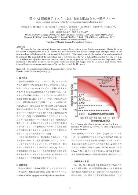
微 小 Al 超 伝 導 ディスクにおける 過 剰 抵 抗 と 単 一 渦 糸 フローExcess resistance and single vortex flow in mesoscopic superconducting Al disk原 田 淳 之A 、 榎 本 健 吾A 、 矢 ヶ 部 太 郎A 、 木 俣 基寺 嶋 太 一A 、 薩 川 秀 隆A A,B、 宇 治 進 也A 、 栗 田 伸 之A 、 硲 香 織A,B 、 小 玉 恒 太A,B 、物 質 ・ 材 料 研 究 機 構A B、 筑 波 大 数 理 物 質Atsushi HARADA A , Kengo ENOMOTO A , Taro YAKABE A , Motoi KIMATA A , Hidetaka SATSUKAWA A ,Nobuyuki KURITA A , Kaori HAZAMA A,B , Kouta KODAMA A,B , Taichi TERASHIMA A , and Shinya UJI A,BA National Institute for Materials Science,B Institute of Material Science, Universitsy of TsukubaAbstract:We report the first observation of Shapiro step response due to a single vortex flow in a mesoscopic Al disk. When anRF current is superimposed on a DC current, we have discovered that periodic voltage steps strikingly appear in thecurrent-voltage (I-V) characteristics near the critical field at L≧1 (L is vorticity, namely, the number of the vortices confinedto a sample). The magnitude of the each voltage step is well reproduced by V n = nφ 0 f ext at the condition f in = nf ext (n = 1, 2,3,…) without any adjustable parameter, where f ext and f in are the frequency of the RF current and the single vortex flow,respectively. This result evidences that the single vortex penetrates and escapes from the Al disk in each period, whichinduces Shapiro step response as the result of the interference with the RF current.Keywords: Mesoscopic superconductor, Excess resistance, Vortex flowE-mail: HARADA.Atsushi@nims.go.jp1. はじめに超 伝 導 性 を 特 徴 づけるコヒーレンス 長 、ロンドン 侵入 長 と 試 料 サイズが 同 程 度 になるメゾスコピック 超 伝導 体 (サブマイクロメータサイズ)では 試 料 の 形 状 ・ 境界 条 件 ( 表 面 )が 超 伝 導 状 態 に 大 きく 影 響 を 与 え、バルクサイズの 試 料 とは 異 なったメゾスコピック 系 特 有 の現 象 が 観 測 される[1]。このメゾスコピック 超 伝 導 において、 超 伝 導 転 移 温 度 (T c ) 近 傍 ではノーマル 状 態 の 抵抗 値 (R n )よりも 電 気 抵 抗 が 高 くなる 過 剰 な 電 気 抵 抗 ( 過剰 抵 抗 )が 観 測 される。ディスク 形 状 の 微 小 Al では 磁 場中 でノーマル 抵 抗 の~8 倍 と 極 めて 大 きな 過 剰 抵 抗 が 報告 されている[2]。この 過 剰 抵 抗 は T c 近 傍 というよりはかなり 広 い 温 度 領 域 でノーマル 抵 抗 よりも 高 い 過 剰 抵 抗 が実 現 している。 過 剰 抵 抗 のディスクサイズ 依 存 性 を 調 べた 研 究 等 により、この 過 剰 抵 抗 は 試 料 内 に 存 在 する 渦 糸が 外 部 電 流 により 渦 糸 フロー 状 態 になることと 関 連 して発 生 しているものと 提 案 されている[3]。バルク 超 伝 導 薄 膜 では、 電 流 駆 動 した 渦 糸 フローと 高周 波 電 流 の 共 鳴 により 電 流 - 電 圧 特 性 において、ジョセフソン 接 合 で 見 られるシャピロステップと 類 似 した、 電 圧ステップが 発 生 することが 知 られている[4,5]。 我 々はこの 電 流 駆 動 させた 渦 糸 フローと 高 周 波 電 流 を 共 鳴 させる測 定 手 法 を 用 いてディスク 形 状 の 微 小 Al 超 伝 導 体 における 渦 糸 フローの 直 接 観 測 を 本 研 究 で 行 った。2. 実 験 方 法微 小 Al 試 料 は、1SiO 2 基 盤 上 にレジスト( 日 本 ゼオン 株 式 会 社 :ZEP520A)を 塗 布 、2 電 子 線 リソグラフィー(Hitachi S4200 equipped with Tokyo Technology BeamFig. 1. Contour plot of the resistance measured with lowfrequency AC current (I ac = 50 nA) for a mesoscopic Al disk0.7 μm in diameter.Draw System)でレジストに 描 画 、3 完 成 したレジストパターンに 高 純 度 のアルミニウム(99.999%)を 蒸 着 、4残 ったレジストを 専 用 溶 剤 で 剥 離 (リフトオフ 工 程 )、上 記 1-4の 工 程 によりディスク 状 の 微 小 Al 試 料 を 作成 する。 本 研 究 では 厚 み 20nm・ 端 子 幅 100nm で 直 径0.7μm の 微 小 Al ディスクを 作 成 し、 最 低 温 度 0.4K・最 大 印 加 磁 場 1000 Oe の 温 度 - 磁 場 領 域 で 測 定 を 行 った。3. 実 験 結 果 と 考 察Fig. 1 は、 厚 み 20nm 端 子 幅 100nm 直 径 0.7μm のディスク 形 状 の 微 小 Al の 電 気 抵 抗 を 様 々な 温 度 - 磁 場 領域 で 測 定 した 結 果 である。 磁 場 はディスク 面 に 垂 直 に印 加 しおり、また 図 中 では 電 気 抵 抗 値 を 色 付 けしてプ- 7 -