DOWNLOAD the Compound Semiconductor Brochure (1.5 MB)
DOWNLOAD the Compound Semiconductor Brochure (1.5 MB)
DOWNLOAD the Compound Semiconductor Brochure (1.5 MB)
Create successful ePaper yourself
Turn your PDF publications into a flip-book with our unique Google optimized e-Paper software.
<strong>Compound</strong><strong>Semiconductor</strong>Solutions
<strong>Compound</strong> <strong>Semiconductor</strong> SolutionsVisible laser diodesVCSELsInfra-red laser diodesEDFAsInfra-red detectorsHigh brightness LEDsThe move from discreet to integrated compound semiconductor devices,Blue LEDsalong with greater demands on linewidth and depth control have allHall Sensorscontributed to shifting both <strong>the</strong> microelectronics and optoelectronicsPower amplifiersindustries from wet etch processing to dry etch processing. The majorLow noise amplifiersadvantage that dry etch offers over wet etch is in <strong>the</strong> choice of ei<strong>the</strong>risotropic or anisotropic processes. Such versatility allows processesranging from sub-micron anisotropic grating etching to isotropic gateGaAs and InP based devices playrecess etching to be carried out in <strong>the</strong> same process chamber.a primary role in high-powersatellite communication systemsDry etching is routinely usedin <strong>the</strong> manufacture of highbrightness blue LEDs and LDsDry etching playsan integral partin <strong>the</strong> manufactureof GaAs poweramplifiers usedin digital handsetsAutomated road traffictoll systems rely onhigh frequency GaAsbased short range radarTo meet <strong>the</strong> demands of <strong>the</strong> industry, Oxford Instruments Plasma Technology provides a fullcomplement of dry process solutions from selective and non-selective mesa etching through tovia hole etching and low damage PECVD. Innovative designs and extensive process development,e.g. low damage gate recess etch by ICP and high quality laser facet coatings, have allcontributed to making OIPT a leading supplier to both <strong>the</strong> micro- and opto-electronic industries.Becoming <strong>the</strong> premier supplier of plasma and ion beam process equipment to <strong>the</strong>compound semiconductor industry can only be achieved through a dedicated focuson <strong>the</strong> quality of our products and customer service support. Our total commitmentto quality, through ISO 9001 qualification, results in excellent product reliability andperformance, thus providing greater machine uptime and lower cost of ownership....making OIPT a leading supplier to both <strong>the</strong> micro- and opto-electronic industries...
MicroelectronicsThrough wafer GaAs based viafeature formed by RIEMESFETs, HEMTs, HFETs and HBTs etc. are all device types thatbenefit from using dry etch technology. The specific benefitsof dry etching over wet etching in <strong>the</strong> manufacture of suchdevices include increased yield, improved uniformitycontrol over 4” and 6" wafers and improved run to runreproducibility. In order to maintain production levelthroughput, wafers are ei<strong>the</strong>r processed through a singlewafer cluster tool, where up to 5 process chambers and onecassette load-lock are integrated around a six way robotichandler, or by batch loading multiple wafers into a singlechamber. Key processes for dry etching in this market are <strong>the</strong>through wafer via hole and <strong>the</strong> low damage selective etchfor gate recess (HEMT) and base contact fabrication (HBT).Through wafer InPbased via featureetched by RIEThe OIPT through wafer via hole process has been developedto provide maximum versatility across a range of processresults and hardware configurations. Both RIE and ICPprocesses are available for GaAs and InP based devices,where via hole shape and roughness can be tailored to meet<strong>the</strong> individual customer requirements. Options include batchprocessing of x4 4" wafers by RIE, providing an effectivethroughput of >1.8 wafers per hour, or a single wafer,4" and 6", high rate ICP process providing an effectivethroughput of >2 wafers per hours.Through waferGaAs based viafeature formedby ICP-RIE...The OIPT process has been developed to provide maximum versatility across a range of process results...GaAs InP GaNLow damage FET basedgate recess etchformed by ICP-RIELow damage gate recess etch ✔ ✔High rate through wafer via etch ✔ ✔Selective mesa etch ✔ ✔ ✔Low damage, lowstress conformalSiN formed by PECVDNon-selective mesa etch ✔ ✔ ✔Metal-contact etch ✔ ✔ ✔Anneal cap PECVD ✔ ✔Capacitor PECVD ✔ ✔Conformal PECVD ✔ ✔ ✔
OptoelectronicsInGaN/GaN mesa etch for high brightnessblue LEDs formed by ICP-RIELow damageInP/InGaAsP basedlaser-diode facetetch formed byICP-RIEDry etching has long been used in <strong>the</strong> fabrication ofoptoelectronic devices, where smooth, vertical feature etchingis required to form electrically and optically isolated mesastructures. Ano<strong>the</strong>r common application for dry etching inoptoelectronics is <strong>the</strong> formation of sub-micron grating structuresin semiconductor lasers. More recently dry etching has beenadopted for <strong>the</strong> fabrication of low damage, high performancelaser facets, where facet verticality and smoothness are criticalparameters affecting device performance and lifetime.OIPT recently completed development of an ICP processspecifically aimed at <strong>the</strong> InP/InGaAsP facet etching market.This process is already in use at a number of production sites on<strong>the</strong> Plasmalab System 100 platform. Results to datedemonstrate laser facet performance comparable to that of acleaved facet.GaAs 220nmgrating formedby RIEGaAs/AlGaAs DBRstructure etch forVCSEL formed by ICP-RIEGaAs based deeplaser-diode facetetch formedby ICP-RIEGaAs InP GaN InSbLaser facet etch ✔ ✔ ✔Sloped profile mesa ✔ ✔ ✔ ✔Selective heterostructure etch ✔ ✔ ✔ ✔Non-selective heterostructure etch ✔ ✔ ✔ ✔Anisotropic etch ✔ ✔ ✔ ✔Isotropic etch ✔ ✔ ✔Sub 0.3 um gratings etch ✔ ✔High quality facet coatings ✔ ✔ ✔Metal-contact etch ✔ ✔ ✔ ✔In addition to semiconductor based etching, OIPT alsoprovides metal and dielectric etching processes for back-enddevice processing. Specifically, processes for gold, titanium andplatinum are available for contact formation as well as siliconnitride and silicon dioxide for masking and isolation.OIPT have also developed a suite of PECVD processesspecifically for optoelectronic device fabrication. Processesinclude, low stress, low damage highly conformal silicon nitride,ammonia-free silicon nitride and low stress silicon dioxide.All processes are developed to meet <strong>the</strong> specific needs of eachcustomer and systems are supplied with process specificationguarantees as standard....<strong>the</strong> Plasmalab System 100 platform...facet performance comparable to that of a cleaved facet...
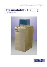
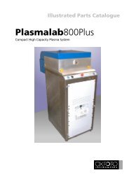
...enabling ourOxford Instruments Plasma Technology supplies a wide range of equipment for use in <strong>the</strong>compound semiconductor market and are <strong>the</strong> only suppliers capable of providing bothplasma and ion beam clustered equipment.The plasma range of equipment includes small stand-alone units, <strong>the</strong> Plasmalab 80 Plus, used forR&D applications and small scale production, through to fully clustered cassette to cassette platforms,Plasmalab System 100, for full scale production. In addition to <strong>the</strong>se two systems, OIPT also suppliesa large area open loaded system, Plasmalab 800 Plus, ideal for batch processing, where up to x12 4"wafers can be processed all at once.The plasma based systems can be configured in four basic modes, namely ICP, RIE, PE and PECVD,which cover <strong>the</strong> main plasma processing configurations. This allows all types of plasmaprocessing to be carried out, e.g. low damage anisotropic etching or low damage photoresist stripwith ICP, anisotropic or isotropic etching by RIE etc..The inductively coupled plasma (ICP) wasadded to <strong>the</strong> Plasmalab range in 1993 and hassince been <strong>the</strong> high density plasma source ofchoice, replacing ECR. The Oxford ICP comesin three sizes, 65mm, 180mm and 380mm, where<strong>the</strong> smallest (ICP65) is used for PECVD andsmall area etching. The ICP180 and <strong>the</strong> ICP380are predominantly used as etch sources, wherea high, controllable ion density at <strong>the</strong> wafersurface is achieved.PlasmalabSystem100The Plasmalab System 100 is a versatile plasma etch and deposition tool from Oxford Instruments Plasma Technology.The design concept follows a modular approach, with individual process modules able to be operated independently,or combined through <strong>the</strong> use of advanced robotic wafer handling. The tool is modular, is MESC compatible and can acceptwafers from 2" through to 8". When clustered, each process module is independently controlled via PLC providingexcellent machine uptime and reliability. The Plasmalab System 100 can be supplied with a range of electrodes andplasma sources ranging from cryogenic electrodes to large area ICP source, making it a highly versatile production tool.
systems to be upgraded in <strong>the</strong> field, thus extending system performance and reliability...Ionfab300PlusPlasmalab80PlusThe Plasmalab 800 Plus is a large-capacity open loadedsystem, configurable for RIE, PE and PECVD. A 460mm diameterelectrode offers a capacity of up to x12 4" wafers or up tox18 3" wafers, ideally suited for batch PECVD processingwhere excellent across chamber uniformity of less than ±2% isachieved for silicon nitride and silicon dioxide layers.The Ionfab 300 Plus is a modular Ionbeam etch and deposition system whichhas cluster capability with <strong>the</strong> PlasmalabSystem 100 via <strong>the</strong> MESC compatiblerobotic handling system. This tool isideally suited for laser facet etching orfor laser facet coatings, where ultrahigh quality Bragg mirrors can be formed.By careful selection and control of <strong>the</strong>stack layer thickness, mirrors for allwavelengths of laser can be fabricated.The Plasmalab 80 Plus, is <strong>the</strong> smallest of<strong>the</strong> tools supplied by OIPT. This systemis ideally suited for R&D or small-scaleproduction where up to x9 2" wafers canbe batch processed on <strong>the</strong> 240mm electrode.The open load design allows for fast loadingand unloading, ideal for prototyping and lowvolume production environments.Plasmalab800PlusValue Added SolutionsTo maximise customer return on investment, Oxford Instruments Plasma Technology offers awide range of value-added programs. These include comprehensive process and servicetraining (to ensure our customers operate at maximum efficiency), a CD-ROM of operatingmanuals and system schematics (for ease of use in cleanroom environments) and hardwareretrofits enabling our systems to be upgraded in <strong>the</strong> field, thus extending system performanceand reliability whilst minimising cost of ownership.SoftwareA Windows based front end software with independent PLC controllers on all modules enablesoff-line maintenance or process development to be carried out without affecting <strong>the</strong> productioncapability of <strong>the</strong> o<strong>the</strong>r modules.
Oxford Instruments Plasma Technology World-wide LocationsOxford Instruments Plasma Technology OfficesRepresentative Agents - For details contact UKUK (Manufacturing)North End, Yatton,Bristol, BS49 4APTel : +44 (0)1934 837000Fax : +44 (0)1934 837001E-mail : plasma.technology@oxinst.co.ukwww.oxford-instruments.com/plmchp5.htmGermanyOtto-von-Guericke Ring 10,65205 WiesbadenTel : +49 (0)6122 937 161Fax : +49 (0)6122 937 175E-mail : plasma@oxford.deJapanHaseman Building2-11-6 TomiokaKoto-Ku, Tokyo 135 - 0047Tel : +81 (0)3 5245 3591Fax : +81 (0)3 5245 4466E-mail : oikkpt@oxford-instruments.ne.jpUSA East Coast130A Baker Avenue,Concord MA 01742.Tel : +1 978 369-9933E-mail : info@ma.oxinst.comUSA West Coast47865 Fremont Blvd,Fremont CA 94538.Tel : +1 510 656 8820Fax : +1 510 656 8944E-mail : info@ma.oxinst.comPeople’s Republic of ChinaOxford Instruments Representative OfficeRoom 508, Instrimpex Building6 Xizhimen Wai StreetXicheng District, Beijing 100044Tel : +86 10 6833 0334/5/6Fax : +86 10 6833 0337SingaporeOxford Instruments Private Limited371 Beach Road, #02-07 KeypointSingapore 199597Tel : +65 6337 6848Fax : +65 6337 6286E-mail : oipt.sales@oxford-instruments.com.sg


