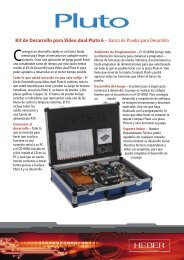
Pluto Document - Heber
Pluto Document - Heber
Pluto Document - Heber
- No tags were found...

Create successful ePaper yourself
Turn your PDF publications into a flip-book with our unique Google optimized e-Paper software.
N500 Hardware Manual<strong>Document</strong> No. 80-20800 Issue 2Current Issue :- 09/07/2009Previous Issues :- 1<strong>Document</strong> No. 80-20800 Issue 2
If your query is not covered in this Manual, or you require further information, please email<strong>Heber</strong> Customer Support: support@heber.co.ukThe latest version of this document and other technical information can be found on the <strong>Heber</strong>website: www.heber.co.ukCopyright © <strong>Heber</strong> Ltd. 2009. All rights reserved. This document and the information containedtherein is the intellectual property of <strong>Heber</strong> Ltd. and must not be disclosed to a third party withoutconsent. Copies may be made only if they are in full and unmodified.The information contained in this document is believed to be accurate and reliable. However, <strong>Heber</strong>Ltd. assumes no responsibility for its use, and reserves the right to revise the documentationwithout notice.Precise specifications may change without prior notice.All trademarks are acknowledged.HEBER LIMITEDBelvedere MillChalford StroudGL6 8NTUKTel +44 (0) 1453 886000Fax +44 (0) 1453 885013Email support@heber.co.ukWebsite www.heber.co.uk<strong>Document</strong> No. 80-20800 Issue 2
Page iCONTENTS1 INTRODUCTION .......................................................................................... 42 N500 FEATURE SUMMARY............................................................................. 53 BOARD LAYOUT ......................................................................................... 73.1 A - CMOS BATTERY .........................................................................................83.2 B – AUDIO AMPLIFIER.........................................................................................83.3 C – BIOS.....................................................................................................83.4 D - INTEL ® 82801GBM (SOUTH BRIDGE)....................................................................83.5 E - DDR2 SODIMM SOCKET.................................................................................83.6 F - INTEL ® 82945GSE (NORTH BRIDGE) ....................................................................83.7 G - EEPROM ................................................................................................83.8 H - CPU (INTEL ® ATOM N270)..............................................................................83.9 I - STANDBY OPERATION BATTERY ...........................................................................83.10 J - CUSTOMER SECURITY DEVICE .............................................................................84 FRONT PANEL CONNECTORS ......................................................................... 94.1 A- COMPACT FLASH SOCKET .................................................................................94.2 B - POWER OUT..............................................................................................94.3 C - VGA1.................................................................................................. 104.4 D, F, G, H - COM1, COM2, COM3, COM4 ............................................................ 104.5 E - VGA2.................................................................................................. 114.6 I AND J – USB ............................................................................................. 114.7 K – ETHERNET.............................................................................................. 124.8 L – PS/2 (MOUSE AND KEYBOARD) ........................................................................ 125 MAIN BOARD CONNECTORS AND JUMPERS .......................................................135.1 A - CMOS CLEAR JUMPER ................................................................................. 145.1.1 Normal Operation................................................................................... 145.1.2 Clear RTC/CMOS .................................................................................... 145.2 B – LEGACY PCI CONNECTOR .............................................................................. 145.3 C – PCIE X 1 ............................................................................................... 145.4 D – COM2 SERIAL SELECTION JUMPERS .................................................................... 145.4.1 RS232 Jumper Setting .............................................................................. 155.4.2 RS485 Jumper Setting .............................................................................. 155.5 E – FRONT PANEL CONNECTORS............................................................................ 165.6 F– USB DOC HEADER...................................................................................... 165.7 G – SATA 1, SATA 2 ..................................................................................... 165.8 H – SATA POWER JUMPER................................................................................. 165.9 I – CASE INTRUSION CONNECTOR ........................................................................... 175.10 J - AUTO POWER ON LINK ................................................................................. 175.11 K, N - FAN1, FAN2 ....................................................................................... 175.12 L – 44W IDE HEADER ...................................................................................... 175.13 M – COMPACT FLASH CONNECTOR.......................................................................... 175.14 O – HARD DISK POWER OUT ............................................................................... 186 IO BLOCK CONNECTORS ..............................................................................196.1 A – AUDIO OUT ............................................................................................ 206.2 B – MIC .................................................................................................... 206.3 C – AUDIO IN............................................................................................... 20<strong>Document</strong> No. 80-20800 Issue 2
Page ii6.4 D – AUDIO STEREO LOUDSPEAKERS ......................................................................... 206.5 E – RS485 TERMINATION .................................................................................. 206.6 F – I/O CONNECTOR 2..................................................................................... 216.7 G – DIL SWITCH ........................................................................................... 226.8 H – CCTALK CHANNEL A ................................................................................... 226.9 I – I/O CONNECTOR 1 ..................................................................................... 236.10 J – CCTALK CHANNEL B.................................................................................... 246.11 K – I/O 3 .................................................................................................. 246.12 L – I/O POWER IN ......................................................................................... 256.13 M –CCTALK CHANNELS A AND B ........................................................................... 256.14 N – 12V POWER IN ........................................................................................ 266.15 O – ATX POWER IN ........................................................................................ 267 BOARD LEDS.............................................................................................278 BIOS UPDATES ..........................................................................................27LIST OF TABLESTable 1 – N500 Board Features ......................................................................................5Table 2 – N500 Environmental Features ...........................................................................6LIST OF FIGURESFigure 1 – Board Layout and Main Components...................................................................7Figure 2 – Front Panel.................................................................................................9Figure 3 – Main Board Connectors and Jumpers ................................................................ 13Figure 4 – I/O Block Connectors................................................................................... 19Figure 5 – LEDs ....................................................................................................... 27<strong>Document</strong> No. 80-20800 Issue 2
Page iiiThis page intentionally left blank.<strong>Document</strong> No. 80-20800 Issue 2
Page 41 INTRODUCTIONThe Nucleus N500 is an Intel ® Atom based integrated gaming control board. The N500 offers thefunctionality of an x86 platform with dedicated gaming Input/Output (I/O). The board has beendesigned to operate with both Linux and Microsoft ® XP Embedded operating systems.This manual gives a detailed description of the Issue 2 hardware platform and board configurationinformation. If you require information that is not covered by this manual please contact <strong>Heber</strong>Technical Support (support@heber.co.uk).<strong>Document</strong> No. 80-20800 Issue 2
Page 52 N500 FEATURE SUMMARYTable 1 – N500 Board FeaturesDimensionsProcessorSystem MemoryChipsetLANGraphicsAudioExpansionPeripheral InterfacesBIOSPowerPower ManagementInputsOutputsBattery Backed SRAM282mm x 206mmIntel ® Atom N270 single core CPU 1.6GHz (soldered directly to the board)1 SODIMM memory socketSingle DDR2 SODIMM Memory module at 400 or 533MHzSupport for up to 1GBIntel ® 945GSE Express Chipset consisting of:82945GSE Graphics and Memory Controller Hub (GMCH)82801GBM I/O Controller Hub (ICH7M)Realtek ® RTL8102E 10/100 Mbit/sec Ethernet with RJ45 connectorIntegrated Intel GMA950 graphics controllerDual video output using 2 independent 15way VGA analogue displayoutputsSupports Windows® Extended desktop mode (Independent displays)Display memory assigned from system memory in BIOSRealtek ALC662 High Definition Audio with 10W Stereo Amplifier for directspeaker connection.Line Level Output, Line Level Input and MIC Level Input 3.5mm Jack.One PCI slotOne PCIe x 1 slot2 SATA interfaces1 IDE 44way interface1 Compact Flash Socket1 Disc on Chip Connector - Silicon Systems (Silicondrive II).4 USB 2.0PS/2 mouse and keyboard ports (fitted to debug boards)3 RS232 serial ports (9way D-types).1 configurable RS232/RS485 serial port (9way D-type).1 configurable RS-232 serial port or ccTalk port1 configurable 5V TTL RS232 serial port or ccTalk portCustom BIOS with user configurable optionsBattery backed CMOS settings4Mb (512KB)Automatic power-on (‘Always on’ Design)20W ATX Power input Connector10W Front panel Power Out connector4W Power Out Connector for Internal Hard Disk Drive4W Power In Connector for I/O BlockAPMI 1.2 – ACPI CompliantReset Watchdog timer – Programmable in BIOS16 general purpose Inputs with +5V pull ups8 Bi-directional, 5V CMOS inputs or 250mA outputs1 8way DIL switches (8 inputs)+12V Current sensed meter supply.4 Power-off inputs (Intrusion / Tamper switches with Time stamp eventlog)PC case open input (Case tamper switch)20 Open drain outputs up to 250mA4 High Current Open drain outputs up to 3A6 5V CMOS outputsDirect support for Starpoint SEC meters512KB user SRAM deviceRechargeable battery - Providing a minimum 90day hold-up time<strong>Document</strong> No. 80-20800 Issue 2
Page 6SecurityRemovable Non-Volatile Data StorageBattery voltage monitoring – to meet GLI-11 specificationDallas electronic serial number (DS2411)Customer specific security device with power-off monitoring of securityswitches, timestamp of events and board unlocking functionsSocketed 32KB I 2 C EEPROMTable 2 – N500 Environmental FeaturesAmbient operating 0-50 degrees CelsiustemperatureRoHSComponents and processes - RoHS compliantCE complianceCE-compliant, meeting the appropriate parts of EN61000 and EN55022Production Life > 5 yearsWarranty1 yearOperational Life > 5 years continuous operation at 50 degrees Centigrade, excludingbatteriesThermalPassive heat cooling for CPU and Chipset<strong>Document</strong> No. 80-20800 Issue 2
Page 73 BOARD LAYOUTThe following figure illustrates the main components on the N500 Control Board.Figure 1 – Board Layout and Main ComponentsA B C D E F G H I JA CMOS BatteryB Audio AmplifierC BIOSD South BridgeE DDR2 SODIMM SocketF North BridgeG EEPROMH CPU (Intel Atom N270)I Standby Operation BatteryJ Customer Security Device<strong>Document</strong> No. 80-20800 Issue 2
Page 83.1 A - CMOS BatteryThe board is fitted with a 3V CR2032 Lithium battery that provides power to the CMOS RAM wherethe BIOS settings are held.3.2 B – Audio AmplifierThe Audio Amplifier provides 10Watt 8ohm stereo output through the Audio Stereo Outputconnector (P1).3.3 C – BIOSThe board is fitted with 4Mb (512KB) SPI EEPROM that contains the system BIOS.3.4 D - Intel ® 82801GBM (South Bridge)The Intel ® 82801GBM is based on the ICH7 controller hub to provide the main board I/O support.3.5 E - DDR2 SODIMM SocketThe board can be fitted with up to 1GB 400MHz or 533MHz DDR2 SODIMM DRAM.3.6 F - Intel ® 82945GSE (North Bridge)The Intel ® 82945GSE manages the flow of information between the system memory interface, theFront Side Bus, the Graphics Interface and the Direct Media Interface (DMI).3.7 G - EEPROM32KB I 2 C EEPROM.3.8 H - CPU (Intel ® Atom N270)The Intel ® Atom N270 1.6GHz CPU main system processor.3.9 I - Standby Operation Battery2.4V Rechargeable Nickel Metal Hydride 70mAh battery that provides power to the security systemwhen the board is powered down.3.10 J - Customer Security DevicePIC16LF819 customer specific security device that provides the following:• Monitoring of security switches when the system is powered down• Customer configurable serial number• Real time clock• Battery Monitoring<strong>Document</strong> No. 80-20800 Issue 2
Page 94 FRONT PANEL CONNECTORSThe Front Panel Connectors are accessible on the front of the board and provide the majority of themain board peripheral interfaces.Figure 2 – Front PanelA B C D E F G H J K LA Compact Flash SocketB Power OutC VGA 1D COM1E VGA 2F COM2G COM3H COM4I USB (x2)J USB (x2)K EthernetL PS/2 Mouse and Keyboard (Development boards only)4.1 A- Compact Flash Socket50 pin standard Compact Flash socket.4.2 B - Power Out10561Pin Signal Description1 12VIO +12V Output2 12VIO +12V Output3 12VIO +12V Output4 12VIO +12V Output5 GND Ground 0V6 GND Ground 0V7 GND Ground 0V8 GND Ground 0V9 5VIO +5V Output10 5VIO +5V Output<strong>Document</strong> No. 80-20800 Issue 2
Page 104.3 C - VGA15115Pin Signal Description1 VGA_R Video Red Output2 VGA_G Video Green Output3 VGA_B Video Blue Output4 NC Not connected5 GND Ground 0V6 GND Ground Input7 GND Ground 0V8 GND Ground 0V9 +5V +5V Output10 GND Ground 0V11 ID0 Monitor ID 0 (Not connected)12 DDC_DATA Display Data Channel Data13 HSYNC Horizontal Synchronisation14 VSYNC Vertical Synchronisation15 DDC_CLK Display Data Channel Clock114.4 D, F, G, H - COM1, COM2, COM3, COM415Pin Signal Description1 DCD Data Carrier Detected (COM2- 485D+)2 RD Receive Data (COM2- 485D-)3 TD Transmit Data (COM2)4 DTR Data Terminal Ready (COM2)5 GND Signal Ground 0V6 DSR Data Set Ready7 RTS Request To Send8 CTS Clear To Send9 RI Ring Indicator6Note: COM2 can be configured as RS232 or RS485 depending on the settings of the jumpers JP4.9<strong>Document</strong> No. 80-20800 Issue 2
Page 114.5 E - VGA25115Pin Signal Description1 VGA_R Video Red Output2 VGA_G Video Green Output3 VGA_B Video Blue Output4 NC Not connected5 GND Ground 0V6 GND Ground 0V7 GND Ground 0V8 GND Ground 0V9 +5V Not connected10 GND Ground11 ID0 Not connected12 DDC_DATA Display Data Channel Data13 HSYNC Horizontal Synchronisation14 VSYNC Vertical Synchronisation15 DDC_CLK Display Data Channel Clock114.6 I and J – USB1 4Pin Signal Description1 VCC +5V2 D- Data -3 D+ Data +4 GND Ground 0V<strong>Document</strong> No. 80-20800 Issue 2
Page 124.7 K – Ethernet81Pin Signal Description1 TX + Transmit Data +2 TX - Transmit Data -3 RX + Receive Data +4 NC Not Connected5 NC Not Connected6 RX - Receive Data -7 NC Not Connected8 NC Not Connected4.8 L – PS/2 (Mouse and Keyboard)642153Pin Signal Description1 DATA Data2 NC Not Connected3 GND Ground 0V4 VCC +5V5 CLK Clock6 NC Not Connected<strong>Document</strong> No. 80-20800 Issue 2
Page 135 MAIN BOARD CONNECTORS AND JUMPERSFigure 3 – Main Board Connectors and JumpersABC DE F GHIJK L M N OA JP1 CMOS Clear JumperB Legacy PCI ConnectorC PCIe x 1D COM2 Serial Selection JumpersE Front Panel ConnectorsF USB DOM HeaderG SATA 1 and SATA 2H SATA Power JumperI Case Intrusion ConnectorJ Auto power on linkK System Fan (2)L 44 way IDE headerM Compact Flash SocketN CPU Fan (1)O Hard Disk Power Out<strong>Document</strong> No. 80-20800 Issue 2
Page 145.1 A - CMOS Clear Jumper15.1.1 Normal OperationUnder normal operation pins 1 and 2 are connected.5.1.2 Clear RTC/CMOSTo clear the RTC/CMOS connect pins 2 and 3.5.2 B – Legacy PCI ConnectorLegacy 32bit PCI expansion connector.5.3 C – PCIe x 1PCI Express x 1 expansion connector.5.4 D – COM2 Serial Selection JumpersCOM2 can be configured as one of the following serial options using the jumpers on header JP4:• RS232• RS485The following sections show the appropriate jumper settings for each mode of operation.<strong>Document</strong> No. 80-20800 Issue 2
Page 155.4.1 RS232 Jumper Setting22212 1• Pins 5-6 closed• Pins 9-19 closed• Pins 10-12 closed• Pins 15-17 closed• Pins 16-18 closed5.4.2 RS485 Jumper Setting22212 1• Pins 1-2 closed• Pins 7-9 closed• Pins 8-10 closed• Pins 19-20 closed<strong>Document</strong> No. 80-20800 Issue 2
Page 165.5 E – Front Panel Connectors121516Pin Signal Description1 5VSB +5V Standby2 NC Not Connected3 NC Not Connected4 NC Not Connected5 SUSLED Suspend LED (cathode)6 NC Not Connected7 NC Not Connected8 NC Not Connected9 NC Not Connected10 5VSB +5V Standby11 NC Not Connected12 POWER_SW Power Switch13 HD_LED Hard Disk LED (anode)14 SYSRST System Reset (active low)15 HD_LED Hard Disk LED (cathode)16 GND Ground5.6 F– USB DOC HeaderUSB Disk-On-Chip connector for Silicon Systems (Silicondrive II).5.7 G – SATA 1, SATA 22 connectors for serial ATA devices.5.8 H – SATA Power Jumper1 3Pins 1 and 2 closed – power to the SATA connectorPins 2 and 3 closed (default) – no power to the SATA connectorThe SATA Power Jumper allows SATA Disk on Modules (DOMs) that can be powered through the SATAconnector to be used. This only powers the right hand connector (J12).<strong>Document</strong> No. 80-20800 Issue 2
Page 175.9 I – Case Intrusion ConnectorPin Signal Description1 CASEOPEN Case Open Signal2 GND Ground 0V3 POFF_SW3 PIC Security Switch 35.10 J - Auto Power On LinkJP6JP7JP81Jumper JP7 closed – default settingJumper JP8 – reserved.5.11 K, N - Fan1, Fan231Pin Signal Description1 GND Ground 0V2 +12V +12 Power3 FAN_IO Fan Speed Pulse Output5.12 L – 44w IDE Header44 way IDE connector for parallel ATA drives.5.13 M – Compact Flash Connector50 pin connector for IDE Compact Flash cards.<strong>Document</strong> No. 80-20800 Issue 2
Page 185.14 O – Hard Disk Power Out41Pin Signal Description1 +12V +12V Output2 GND Ground 0V3 GND Ground 0V4 VCC +5V Output<strong>Document</strong> No. 80-20800 Issue 2
Page 196 IO BLOCK CONNECTORSFigure 4 – I/O Block ConnectorsABC D E F G H I J K LM N OA Audio (line) OutB MicC Audio (line) InD Audio Stereo LoudpseakersE RS485 TerminationF I/O 2G DIL Switch (x 8)H CCTalk Channel AI I/O 1J CCTalk Channel BK I/O 3L I/O Power InM CCTalk Channels A and BN Power InO ATX Power In<strong>Document</strong> No. 80-20800 Issue 2
Page 206.1 A – Audio OutLine Level Output audio connection – 3.5mm Stereo Jack.6.2 B – MICMIC Level Input audio connection – 3.5mm Stereo Jack.6.3 C – Audio InLine Level Input audio connection – 3.5mm Stereo Jack.6.4 D – Audio Stereo Loudspeakers10 Watt Amplified stereo audio output (8 ohms).41Pin Signal Description1 LS/R+ Loud Speaker Right Positive2 LS/R- Loud Speaker Right Negative3 LS/L+ Loud Speaker Left Positive4 LS/L- Loud Speaker Left Negative6.5 E – RS485 TerminationIf COM2 is used for RS232 the pins should be left open.If RS485 termination is required the pins should be closed with a jumper.<strong>Document</strong> No. 80-20800 Issue 2
Page 216.6 F – I/O Connector 2Pin Signal Description1 OP16 Open Drain Output 162 OP17 Open Drain Output 173 OP18 Open Drain Output 184 OP19 Open Drain Output 195 OP20 Open Drain Output 206 OP21 Open Drain Output 217 OP22 Open Drain Output 228 OP23 Open Drain Output 239 OP24 Open Drain Output 2410 OP25 Open Drain Output 2511 OP26 Open Drain Output 2612 OP27 Open Drain Output 2713 OP28 High Current Output 28 *14 OP28 High Current Output 28 *15 OP29 High Current Output 29 *16 OP28 High Current Output 28 *17 OP29 High Current Output 29 *18 OP29 High Current Output 29 *19 OP30 High Current Output 30 *20 OP30 High Current Output 30 *21 OP31 High Current Output 31 *22 OP30 High Current Output 30 *23 OP31 High Current Output 31 *24 OP31 High Current Output 31 *25 IP6 Input 626 IP7 Input 727 IP8 Input 828 IP9 Input 929 IP10 Input 1030 IP11 Input 1131 IP12 Input 1232 IP13 Input 1333 IP14 Input 1434 IP15 Input 1535 12VIO +12v Output36 12VIO +12v Output37 12VIO +12v Output38 12VIO +12v Output39 GND Ground 0V40 GND Ground 0V41 GND Ground 0V42 GND Ground 0V43 GND Ground 0V44 GND Ground 0V45 POFF_COM Security Switch Common46 GND Ground 0V47 POFF_SW0 Security Switch 148 POFF_SW1 Security Switch 249 POFF_SW2 Security Switch 350 POFF_SW3 Security Switch 4<strong>Document</strong> No. 80-20800 Issue 2
Page 22* Duplicated outputs can be used in parallel where a current capacity greater than 1Amp isrequired.6.7 G – DIL SwitchSoftware readable 8way DIL switch.6.8 H – CCtalk Channel A21109Pin Signal Description1 CCA_DATA CCtalk Channel A data2 GND Ground 0V3 CCA_BUSY CCtalk Channel A busy4 GND Ground 0V5 OP8 CCtalk Channel A Reset (Output 8)6 N/C Not Connected7 12VIO +12V8 GND Ground 0V9 GND Ground 0V10 12VIO +12V<strong>Document</strong> No. 80-20800 Issue 2
Page 236.9 I – I/O Connector 1Pin Signal Description1 OP0/IP16 Open Drain Output 0/Input 162 OP1/IP17 Open Drain Output 1/Input 173 OP2/IP18 Open Drain Output 2/Input 184 OP3/IP19 Open Drain Output 3/Input 195 OP4/IP20 Open Drain Output 4/Input 206 OP5/IP21 Open Drain Output 5/Input 217 OP6/IP22 Open Drain Output 6/Input 228 OP7/IP23 Open Drain Output 7/Input 239 OP8 Open Drain Output 810 OP9 Open Drain Output 911 OP10 Open Drain Output 1012 OP11 Open Drain Output 1113 OP12 Open Drain Output 1214 OP13 Open Drain Output 1315 OP14 Open Drain Output 1416 OP15 Open Drain Output 1517 IP0 Input 018 IP1 Input 119 IP2 Input 220 IP3 Input 321 IP4 Input 422 IP5 Input 523 V_METER +12v Sensed Current24 12VIO +12v25 GND Ground 0V26 GND Ground 0V27 LS/L+ Input 828 LS/R+ Input 929 LS/L- Input 1030 LS/R- Input 1131 GND Ground 0V32 GND Ground 0V33 NC Not Connected34 NC Not Connected<strong>Document</strong> No. 80-20800 Issue 2
Page 246.10 J – CCtalk Channel B21109Pin Signal Description1 CCB_DATA CCtalk Channel B data2 GND Ground 0V3 CCB_BUSY CCtalk Channel B busy4 GND Ground 0V5 OP9 CCtalk Channel B Reset (Output 9)6 N/C Not Connected7 12VIO +12V8 GND Ground 0V9 GND Ground 0V10 12VIO +12V6.11 K – I/O 3211615Pin Signal Description1 GND Ground 0V2 GND Ground 0V3 RS232A_RX RS232 channel A receive4 RS232A_TX RS232 channel A transmit5 RS232A_CTS RS232 channel A clear to send6 RS232A_RTS RS232 channel A ready to send7 TTL_RX TTL level receive8 TTL_TX TTL level transmit9 12VIO +12 volt output10 -12v -12 volt output11 AUX0 Auxiliary output 012 AUX1 Auxiliary output 113 AUX2 Auxiliary output 214 AUX3 Auxiliary output 315 AUX4 Auxiliary output 416 AUX5 Auxiliary output 5<strong>Document</strong> No. 80-20800 Issue 2
Page 256.12 L – I/O Power InPin Signal Description1 12VIO +12V Input2 GND Ground 0V3 GND Ground 0V4 5VIO +5V Input6.13 M –CCTalk Channels A and B21Pin Signal Description1 CCA_DATA CCtalk Channel A data2 GND Ground 0V3 CCA_BUSY CCtalk Channel A busy4 GND Ground 0V5 OP8 CCtalk Channel A Reset (Output 8)6 N/C Not Connected7 12VIO +12V8 GND Ground 0V9 GND Ground 0V10 12VIO +12V11 CCB_DATA CCtalk Channel B data12 GND Ground 0V13 CCB_BUSY CCtalk Channel B busy14 GND Ground 0V15 OP9 CCtalk Channel B Reset (Output 9)16 N/C Not Connected17 12VIO +12V18 GND Ground 0V19 GND Ground 0V20 12VIO +12V<strong>Document</strong> No. 80-20800 Issue 2
Page 266.14 N – 12V Power In1324Pin Signal Description1 GND Ground 0V2 GND Ground 0V3 12V +12V Input4 12V +12V Input6.15 O – ATX Power In1 1011 20Pin Signal Description1 VCC3 +3.3V2 VCC3 +3.3V3 GND Ground 0V4 VCC +5V5 GND Ground 0V6 VCC +5V7 GND Ground 0V8 PW_OK Power Good Signal9 5VSB +5V Standby10 +12V +12V11 VCC3 +3.3V12 -12V -12V13 GND Ground14 PS_ON Power Supply On15 GND Ground 0V16 GND Ground 0V17 GND Ground 0V18 -5V -5V19 VCC +5V20 VCC +5V<strong>Document</strong> No. 80-20800 Issue 2
Page 277 BOARD LEDSFigure 5 – LEDsABCDEFGABCDEFGHard Disk ActivityI/O Processor Active+5V IO Block Power Indicator+12V IO Block Power Indicator+3V Main Board Power Indicator+5V Main Board Power Indicator+12V Main Board Power Indicator8 BIOS UPDATESBIOS updates will be posted on the <strong>Heber</strong> Web site for download along with programminginstructions.<strong>Document</strong> No. 80-20800 Issue 2