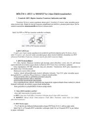
TDA7240 - 320Volt
TDA7240 - 320Volt
TDA7240 - 320Volt
- No tags were found...

You also want an ePaper? Increase the reach of your titles
YUMPU automatically turns print PDFs into web optimized ePapers that Google loves.
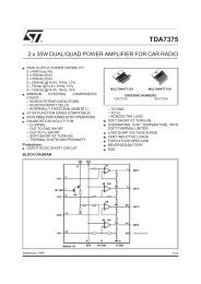
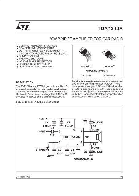
®<strong>TDA7240</strong>ACOMPACT HEPTAWATT PACKAGEFEW EXTERNAL COMPONENTSOUTPUT PROTECTED AGAINST SHORTCIRCUITS TO GROUND AND ACROSS LOADDUMP TRANSIENTTHERMAL SHUTDOWN.LOUDSPEAKER PROTECTIONHIGH CURRENT CAPABILITYLOW DISTORTION/LOW NOISEHeptawatt HORDERING NUMBERS:Heptawatt V20W BRIDGE AMPLIFIER FOR CAR RADIO<strong>TDA7240</strong>AH<strong>TDA7240</strong>AVDESCRIPTIONThe <strong>TDA7240</strong>A is a 20W bridge audio amplifier ICdesigned specially for car radio applications.Thanks to the low external part count and compactHeptawatt 7-pin power package the <strong>TDA7240</strong>Aoccupies little space on the printed circuit board.Reliable operation is guaranteed by a comprehensivearray of on-chip protection features. These includeprotection against AC and DC output shortcircuits (to groundand across the load), load dumptransients, and junction overtemperature. Additionally,the<strong>TDA7240</strong>Aprotectstheloudspeakerwhenone output is short-circuited to ground.Figure 1: Test and Application CircuitDecember 19981/8
<strong>TDA7240</strong>APIN CONNECTION (Top view)ABSOLUTE MAXIMUM RATINGSSymbol Parameter Value UnitVs Operating Supply Voltage 18 VV s DC Supply Voltage 28 VV s Peak Supply Voltage (for 50ms) 40 VI o (*) Peak Output Current (non repetitive t = 0.1ms) 4.5 AI o (*) Peak Output Current (repetitive f ≥10Hz) 3.5 AP tot Power Dissipation at Tcase = 85°C 16 WT stg ,T j Storage and Junction Temperature –40 to 150 °C(*) Internally limitedTHERMAL DATASymbol Parameter Value UnitR th j-case Thermal Resistance Junction-case Max. 4 V2/8
ELECTRICAL CHARACTERISTICS (refer to the circuit of fig. 1, Tamb =25°C, Rth (heatsink)= 4°C/W,Vs = 14.4V)Symbol Parameter Test Conditions Min. Typ. Max. UnitV s Supply Voltage 18 VV os Output Offset Voltage 150 mVI d Total Quiescent Current R L =4Ω 65 120 mAP o Output Power f = 1kHz; d = 10%R L =4ΩR L =8Ω18102012WWd Distortion R L =4Ω f = 1kHz0.1 0.5 %P o = 50mW to 12WR L =8Ωf = 1kHz0.05 0.5 %P o = 50mW to 12WGV Voltage Gain f = 1KHz 39.5 40 40.5 dBSVR Supply Voltage Rejection f = 100Hz R g = 10KΩ 35 40 dBE N Total Input Noise R g = 10KΩ(*)(**)23 10<strong>TDA7240</strong>Aη Efficiency R L =4Ω f = 1KHz 65 %I sb Stand-by Current 200 µAR i Input Resistance f = 1kHz 70 kΩV i Input Sensitivity f = 1kHz; P o = 2W; R L =4Ω 28 mVf L Low Frequency Roll Off Po = 15W; R L =4Ω 30 Hz(–3dB)f H High Frequency Roll Off Po = 15W; RL = 4Ω 25 kHz(–3dB)A s Stand-by Attenuation V o = 2Vrms 70 90 dBV TH (pin2) Stand-by Threshold 1 V(*) B= Curve A (**) B = 22Hz to 22 KHzµVµVFigure2:P.C. Board and Components layout of the Circuit of Fig. 1.(1:1scale)3/8
<strong>TDA7240</strong>AAPPLICATION SUGGESTIONThe recommendedvalues of thecomponentsare thoseshownon applicationcircuit of Fig.1. Differentvaluescan be used, the following table can help the designer.Component RecommendedPurpose Larger Than Smaller ThanValueR1, R2 2.2Ω Frequency Stability Danger of HighFrequency OscillationC1 1µF Input DC Decoupling Higher Turn On andStand-by DelayC2 22µF Ripple Rejection Increase of SVRIncrease of the TurnOn DelayC3 22µF Feedback lowFrequency CutoffHigher Turn On Pop.Higher LowFrequency CutoffDegradation of SVRHigher Low FrequencyCutoffC6, C7 0.22µF Frequency Stability Danger of OscillationC4 220µF Supply Filter Danger of OscillationC5 0.1µF Supply Bypass Danger of OscillationFigure 3 : OutputPower vs. Supply Voltage.Figure 4 : Distortion vs. Output Power.Figure 5 : Output Power vs. Supply voltage.Figure 6 : Distortion vs. Output Power.4/8
<strong>TDA7240</strong>AFigure 7 : Distortion vs. Frequency.Figure 8 : SupplyVoltage Rejectionvs. Frequency.Figure 9 : Power Dissipation and Efficiency vs.Output Power.Figure 10 : PowerDissipation and Efficiency vs.Output Power.5/8
<strong>TDA7240</strong>ADIM.mminchMIN. TYP. MAX. MIN. TYP. MAX.A 4.8 0.189C 1.37 0.054D 2.4 2.8 0.094 0.110D1 1.2 1.35 0.047 0.053E 0.35 0.55 0.014 0.022E1 0.7 0.97 0.028 0.038F 0.6 0.8 0.024 0.031F1 0.9 0.035G 2.34 2.54 2.74 0.095 0.100 0.105G1 4.88 5.08 5.28 0.193 0.200 0.205G2 7.42 7.62 7.82 0.295 0.300 0.307H2 10.4 0.409H3 10.05 10.4 0.396 0.409L 16.7 16.9 17.1 0.657 0.668 0.673L1 14.92 0.587L2 21.24 21.54 21.84 0.386 0.848 0.860L3 22.27 22.52 22.77 0.877 0.891 0.896L4 1.29 0.051L5 2.6 2.8 3 0.102 0.110 0.118L6 15.1 15.5 15.8 0.594 0.610 0.622L7 6 6.35 6.6 0.236 0.250 0.260L9 0.2 0.008M 2.55 2.8 3.05 0.100 0.110 0.120M1 4.83 5.08 5.33 0.190 0.200 0.210V440° (typ.)Dia 3.65 3.85 0.144 0.152OUTLINE ANDMECHANICAL DATAHeptawatt VLL1EVVM1ACD1L2DMH2L5L3EFE1L9V4H3H1G G1 G2Dia.L7L4H2F1FL6HEPTAMEC6/8
<strong>TDA7240</strong>ADIM.mminchMIN. TYP. MAX. MIN. TYP. MAX.A 4.8 0.189C 1.37 0.054D 2.4 2.8 0.094 0.110D1 1.2 1.35 0.047 0.053E 0.35 0.55 0.014 0.022F 0.6 0.8 0.024 0.031F1 0.9 0.035G 2.41 2.54 2.67 0.095 0.100 0.105G1 4.91 5.08 5.21 0.193 0.200 0.205G2 7.49 7.62 7.8 0.295 0.300 0.307H2 10.4 0.409H3 10.05 10.4 0.396 0.409L 14.2 0.559L1 4.4 0.173L2 15.8 0.622L3 5.1 0.201L5 2.6 3 0.102 0.118L6 15.1 15.8 0.594 0.622L7 6 6.6 0.236 0.260L9 4.44 0.175Dia 3.65 3.85 0.144 0.152OUTLINE ANDMECHANICAL DATAHeptawatt H7/8
<strong>TDA7240</strong>AInformation furnished is believed to be accurate and reliable. However, STMicroelectronics assumes no responsibility for the consequencesof use of such information nor for any infringement of patents or other rights of third parties which may result from its use. Nolicense is granted by implication or otherwise under any patent or patent rights of STMicroelectronics. Specification mentioned in thispublication are subject to change without notice. This publication supersedes and replaces all information previously supplied. STMicroelectronicsproducts are not authorized for use as critical components in life support devices or systems without express writtenapproval of STMicroelectronics.The ST logo is a registered trademark of STMicroelectronicsHEPTAWATT is a Trademark of SGS-THOMSON Microelectronics© 1998 STMicroelectronics – Printed in Italy – All Rights ReservedSTMicroelectronics GROUP OF COMPANIESAustralia - Brazil - Canada - China - France - Germany - Italy - Japan - Korea - Malaysia - Malta - Mexico - Morocco - The Netherlands -Singapore - Spain - Sweden - Switzerland - Taiwan - Thailand - United Kingdom - U.S.A.http://www.st.com8/8