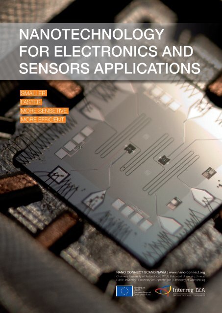
Nanotechnology for Electronics and Sensors Applications
Nanotechnology for Electronics and Sensors Applications
Nanotechnology for Electronics and Sensors Applications

Create successful ePaper yourself
Turn your PDF publications into a flip-book with our unique Google optimized e-Paper software.
NANOTECHNOLOGY<br />
FOR ELECTRONICS AND<br />
SENSORS APPLICATIONS<br />
SMALLER<br />
FASTER<br />
MORE SENSETIVE<br />
MORE EFFICIENT<br />
NANO CONNECT SCANDINAVIA | www.nano-connect.org<br />
Chalmers University of Technology | DTU | Halmstad University | Imego<br />
Lund University | University of Copenhagen | University of Gothenburg<br />
1
<strong>Nanotechnology</strong> <strong>for</strong> <strong>Electronics</strong> <strong>and</strong> <strong>Sensors</strong> <strong>Applications</strong><br />
2<br />
0.142 nm<br />
Carbon-Carbon bond length in<br />
graphene: 0.142 nm<br />
22 nm<br />
The length of a transistor gate in the<br />
latest CPU technology from Intel: 22 nm<br />
Why nanotechnology matters<br />
The advances in nanotechnology have brought new tools<br />
to the field of electronics <strong>and</strong> sensors. New designed<br />
materials offer new <strong>and</strong> unique properties enabling the<br />
development <strong>and</strong> cost efficient production of state-of-theart<br />
components that operate faster, has higher sensitivity,<br />
consume less power, <strong>and</strong> can be packed at much higher<br />
densities.<br />
Numerous products based on nanotechnology have been<br />
reaching the market <strong>for</strong> some years, all the way to end<br />
users <strong>and</strong> consumers. For instance, at the nanoscale, the<br />
resistance dependence of a material on an external magnetic<br />
field is significantly amplified, which has led to the<br />
fabrication of hard disks with a data storage density in the<br />
gigabyte <strong>and</strong> terabyte ranges. <strong>Nanotechnology</strong> has also<br />
enabled the development of sensors suitable <strong>for</strong> measurements<br />
at the molecular level with an unprecedented sensitivity<br />
<strong>and</strong> response time, mainly due to their high surface<br />
to volume ratio.<br />
With this brochure Nano Connect Sc<strong>and</strong>inavia, an EUfinanced<br />
project representing seven universities <strong>and</strong> institutes<br />
in south-western Sc<strong>and</strong>inavia, presents a few promising<br />
areas of nanoelectronics <strong>and</strong> nanosensors.<br />
400 nm<br />
740 nm<br />
Track pitch<br />
The size of a single bit of in<strong>for</strong>mation<br />
on a DVD disk: 400 nm<br />
WHAT IS NANOTECHNOLOGY?<br />
<strong>Nanotechnology</strong> is the underst<strong>and</strong>ing<br />
<strong>and</strong> control of matter <strong>and</strong> processes<br />
at the nanoscale, typically, but not exclusively,<br />
below 100 nanometres in one<br />
or more dimensions where the onset<br />
of size-dependent phenomena usually<br />
enables novel applications. <strong>Nanotechnology</strong><br />
is cross-disciplinary in nature,<br />
drawing on medicine, chemistry, biology,<br />
physics <strong>and</strong> materials science.<br />
New properties<br />
At the nanoscale, matter begins to<br />
demonstrate entirely new <strong>and</strong> unique<br />
properties. It can become stronger,<br />
conduct heat better, <strong>and</strong> show extraordinary<br />
electrical properties.<br />
Creating nanostructures<br />
With a bottom-up approach, nanostructures<br />
are <strong>for</strong>med molecule by molecule,<br />
using methods such as chemical<br />
vapour deposition or self-assembly. By<br />
contrast, top-down fabrication can be<br />
likened to sculpting from a base material,<br />
<strong>and</strong> typically involves steps such as<br />
deposition of thin films, patterning, <strong>and</strong><br />
etching.
A true example of nanotechnology: an<br />
array of individually addressable vertically-aligned<br />
carbon nanofibers <strong>for</strong><br />
sensing applications at the nanoscale.<br />
For comparison, a single human hair is<br />
1000 times thicker than any of the nanofibers<br />
in the image. (Image courtesy<br />
of Farzan Alavian Ghavanini, Chalmers<br />
University of Technology)<br />
CARBON-BASED SENSORS AND ELECTRONICS<br />
The semiconductor industry has been able to improve the per<strong>for</strong>mance of electronic systems <strong>for</strong> more<br />
than four decades by downscaling silicon-based devices but this approach will soon encounter its<br />
physical <strong>and</strong> technical limits. This fact, together with increasing requirements <strong>for</strong> per<strong>for</strong>mance, functionality,<br />
cost, <strong>and</strong> portability have been driven the microelectronics industry towards the nano world<br />
<strong>and</strong> the search <strong>for</strong> alternative materials to replace silicon. Carbon nanomaterials such as one-dimensional<br />
(1D) carbon nanotubes <strong>and</strong> two-dimensional (2D) graphene have emerged as promising options<br />
due to their superior electrical properties which allow <strong>for</strong> fabrication of faster <strong>and</strong> more power-efficient<br />
electronics. At the same time their high surface to volume ratio combined with their excellent mechanical<br />
properties has rendered them a robust <strong>and</strong> highly sensitive building block <strong>for</strong> nanosensors.<br />
Graphene transistor<br />
In 2004, it was shown <strong>for</strong> the first time that a single sheet of carbon atoms packed in a honeycomb<br />
crystal lattice can be isolated from graphite <strong>and</strong> is stable at room temperature. The new nanomaterial,<br />
which is called graphene, allows electrons to move at an extraordinarily high speed. This property,<br />
together with its intrinsic nature of being one-atom-thick, can be exploited to fabricate field-effect transistors<br />
that are faster <strong>and</strong> smaller.<br />
A layer of graphene acts as the conducting<br />
channel in a field-effect transistor.<br />
3
<strong>Nanotechnology</strong> <strong>for</strong> <strong>Electronics</strong> <strong>and</strong> <strong>Sensors</strong> <strong>Applications</strong><br />
4<br />
Carbon nanotube electronics<br />
When a layer of graphene is rolled into a tube,<br />
a single-walled carbon nanotube (SWNT) is<br />
<strong>for</strong>med. Consequently, SWNTs inherit the<br />
attractive electronic properties of graphene<br />
but their cylindrical structure makes them a<br />
more readily available option <strong>for</strong> <strong>for</strong>ming the<br />
channel in field-effect transistors. Such transistors<br />
possess an electron mobility superior<br />
to their silicon-based counterpart <strong>and</strong> allow<br />
<strong>for</strong> larger current densities while dissipating<br />
the heat generated from their operation more<br />
efficiently. During the last decade, carbon<br />
nanotube-based devices have advanced beyond<br />
single transistors to include more complex<br />
systems such as logic gates <strong>and</strong> radiofrequency<br />
components.<br />
Carbon-based nanosensors<br />
In addition to the exceptional electrical properties<br />
of graphene <strong>and</strong> carbon nanotubes,<br />
their excellent thermal conductivity, high mechanical<br />
robustness, <strong>and</strong> very large surface<br />
to volume ratio make them superior materials<br />
<strong>for</strong> fabrication of electromechanical <strong>and</strong><br />
electrochemical sensors with higher sensitivities,<br />
lower limits of detection, <strong>and</strong> faster<br />
response time. A good example is the carbon<br />
nanotube-based mass sensor that can<br />
detect changes in mass caused by a single<br />
gold atom adsorbing on its surface.<br />
An artistic expression of an integrated circuit based on individual<br />
carbon nanotubes.<br />
(Image courtesy of Cees Dekker, TU Delft / Tremani)<br />
Any additional gold atom that adsorbs on<br />
the surface of a vibrating carbon nanotube<br />
would change its resonance frequency which<br />
is further detected. (Image courtesy of Zettl<br />
Research Group, Lawrence Berkeley National<br />
Laboratory <strong>and</strong> University of Cali<strong>for</strong>nia at<br />
Berkeley)
MOLECULAR ELECTRONICS<br />
Recent advances in nanofabrication techniques have provided the opportunity to use single molecules,<br />
or a tiny assembly of them, as the main building blocks of an electronic circuit. This, combined with<br />
the developed tools of molecular synthesis to engineer basic properties of molecules, has enabled the<br />
realisation of novel functionalities beyond the scope of traditional solid state devices.<br />
Single Molecule Memory Device<br />
A modern memory device, in its most common implementation, stores each bit of data by charging up<br />
a tiny capacitor. The continuous downscaling of electronic circuits, in this context, translates to storing<br />
less charge in a smaller capacitor. Ultimately, as memory device dimensions approach the nanometer<br />
range, the capacitor can be replaced by a single organic molecule such as Ferrocene, whose oxidation<br />
state can be altered by moving an electron into or out of the molecule.<br />
A neutral Ferrocene molecule is<br />
attached to a nanoelectrode representing<br />
a “0” state.<br />
An electron tunnels to the nanoelectrode<br />
by the application of an external<br />
electrical field.<br />
The positively charged Ferrocene<br />
molecule represents a “1” state.<br />
Organic Transistor Odour Sensor<br />
Organic field-effect transistors (OFETs) are a good example of the scope of traditional electronic devices<br />
being augmented by the chemical reactivity of an organic semiconductor material in their channel.<br />
In an odour sensor, <strong>for</strong> instance, the nano-scale chemical reactions upon exposure of the device to a<br />
certain atmospheric condition modify the electronic properties of the organic semiconducting material<br />
which is further reflected by a change in the current flowing through the transistor.<br />
5
<strong>Nanotechnology</strong> <strong>for</strong> <strong>Electronics</strong> <strong>and</strong> <strong>Sensors</strong> <strong>Applications</strong><br />
QUANTUM COMPUTING<br />
The excitement in the field of quantum computing was triggered<br />
in 1994 by Peter Shor who showed how a quantum algorithm<br />
could exponentially speed up a classical computation. Such algorithms<br />
are implemented in a device that makes direct use of<br />
quantum mechanical phenomena such as entanglement <strong>and</strong> superposition.<br />
Since the physical laws that govern the behaviour of<br />
a system at the atomic scale are inherently quantum mechanical<br />
in nature, nanotechnology has emerged as the most appropriate<br />
tool to realise quantum computers.<br />
Quantum computing chip: the two black squares are the quantum bits or qubits,<br />
the processing centre; the me<strong>and</strong>ering line at the centre is the quantum bus;<br />
<strong>and</strong> the lateral me<strong>and</strong>ering lines are the quantum memory. (Image courtesy of<br />
Erik Lucero)<br />
SINGLE ELECTRON TRANSISTOR<br />
In contrast to common transistors, where the switching action requires<br />
thous<strong>and</strong>s of electrons, a single electron transistor needs<br />
only one electron to change from the insulating to the conducting<br />
state. Such transistors can potentially deliver very high device<br />
density <strong>and</strong> power efficiency with remarkable operational speed.<br />
In order to implement single electron transistors, extremely small<br />
metallic isl<strong>and</strong>s with sub-100 nm dimensions have to be fabricated.<br />
These isl<strong>and</strong>s, which are referred to as quantum dots, can<br />
be fabricated by employing processes made available by the advances<br />
in nanotechnology.<br />
A single electron transistor in a surface acoustic wave echo chamber<br />
(Image courtesy of Philip Krantz, Chalmers University of Technology)<br />
SPINTRONICS<br />
Similar to electrical charge, spin is another fundamental property<br />
of matter. While conventional electronic devices rely on the<br />
transport of electrical charge carriers, the emerging technology<br />
of spintronics employs the spin of electrons to encode <strong>and</strong><br />
transfer in<strong>for</strong>mation. Spintronics has the potential to deliver nanoscale<br />
memory <strong>and</strong> logic devices which process in<strong>for</strong>mation<br />
faster, consume less power, <strong>and</strong> store more data in less space.<br />
The extension of the hard disk capacities to the gigabyte <strong>and</strong> the<br />
terabyte ranges was the main achievement of spintronics by taking<br />
advantage of Giant Magneto-Resistance (GMR) <strong>and</strong> Tunnel<br />
Magneto-Resistance (TMR) effects which are effective only at the<br />
nano scale.<br />
A close-up look at a hard disk drive improved with the Giant Magneto-Resistance<br />
technology<br />
6
NANO-ELECTRO-MECHANICAL SYSTEMS (NEMS)<br />
All electronic tools have one thing in common: an integrated circuit (IC) acting as their “brain”. The<br />
extent to which this “brain” has influenced our lives has already been tremendous but what if its<br />
decision-making capability is augmented by “eyes” <strong>and</strong> “arms”? Nano-electro-mechanical systems<br />
have evolved during the last 10 years to make this dream come true by creating sensors (“eyes”) <strong>and</strong><br />
actuators (“arms”) at the same scale as the accompanying nanoelectronics. Recent developments<br />
in synthesis of nanomaterials with excellent electrical <strong>and</strong> mechanical properties have extended the<br />
boundaries of NEMS applications to include more advanced devices such as the non-volatile nanoelectro-mechanical<br />
memory, where in<strong>for</strong>mation is transferred <strong>and</strong> stored through a series of electrical<br />
<strong>and</strong> mechanical actions at the nanoscale.<br />
A carbon based nano-electro-mechanical<br />
nonvolatile memory;<br />
A. Separated CNTs<br />
represents a ‘0’ state.<br />
A.<br />
D. Applying a relatively large<br />
voltage across the junction<br />
generates CNT phonon excitations<br />
with sufficient energy to<br />
cause their separation leading<br />
to the RESET operation.<br />
B.<br />
D.<br />
B. CNTs are brought into<br />
contact by applying a<br />
voltage between them.<br />
C.<br />
C. Contacted CNTs<br />
represents a ‘1’ state.<br />
Would you like to know more?<br />
This brochure is part of a series, covering different application areas of nanotechnology, including life<br />
science, materials, electronics & sensors, <strong>and</strong> the regulatory framework <strong>for</strong> nanomaterials. Please visit<br />
www.nano-connect.org <strong>for</strong> more in<strong>for</strong>mation.<br />
This work was supported by the EU through its Interreg IVA Programme. It reflects only the author’s views. The Community<br />
is not liable <strong>for</strong> any use that may be made of the in<strong>for</strong>mation contained therein.<br />
7
<strong>Nanotechnology</strong> <strong>for</strong> <strong>Electronics</strong> <strong>and</strong> <strong>Sensors</strong> <strong>Applications</strong><br />
Connecting people who<br />
think<br />
big<br />
about very<br />
small<br />
things<br />
Chalmers University of Technology<br />
Halmstad University<br />
Imego<br />
Lund University<br />
Technical University of Denmark<br />
University of Copenhagen<br />
University of Gothenburg<br />
Hall<strong>and</strong> Regional Development Council<br />
Region Skåne<br />
Region Västra Götal<strong>and</strong><br />
Region Zeal<strong>and</strong><br />
The Capital Region of Denmark<br />
Nano Connect Sc<strong>and</strong>inavia<br />
www.nano-connect.org<br />
Download this <strong>and</strong> other brochures from<br />
www.nano-connect.org/downloads<br />
8