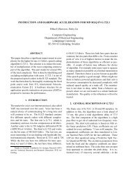
able part which writes the PC <strong>and</strong> the outputs <strong>and</strong> the input bufferto a file every clock cycle <strong>for</strong> verification purposes only. For allinput combinations, corresponding reference files were manuallycreated in order to simplify the verification task.OutputsData InputThis covers most of the RTL code, but of course the coverage isnot 100%. Control signals that do not interfere were not tested inall combinations <strong>and</strong> all data patterns were not used, since thatwould have required too much time.5.2. Formal Functions VerificationFor the verification of the <strong>for</strong>mal functions, the example programfrom section 4 was used. It covers the following functions as basic<strong>and</strong> kernel functions <strong>for</strong> a general purpose protocol processor:• Synchronize the processing based on in<strong>for</strong>mation from thephysical interface• Match packet header field to several acceptable values• Demultiplex packet processing based on upper layer protocol• Use checksums to assure that no transmission errors haveoccurred• H<strong>and</strong> over a correct packet payload to the application processingThe reception processing was first modelled in C++ at a behaviorallevel. Then a structural C++ model was developed, which executesthe instruction set in a cycle true manner. The simulation needsfour inputs, the ILT content, the PCB content, the CCB content <strong>and</strong>the received packet. The structural model was then manually transferredinto a VHDL model, which is used <strong>for</strong> implementation. Thetestbench <strong>for</strong> the VHDL model use the same stimuli files as theC++ model <strong>and</strong> thereby the VHDL was verified efficiently.5.3. Error InjectionTo make sure that the PP executes all program branches correctly,packets with various errors were injected into the simulation.These faulty packets cover the following errors:• Ethernet destination address that is not <strong>for</strong> the host• IP destination address that is not <strong>for</strong> the host• Ethernet code which is not IP or ARP• IP protocol which is not UDP• UDP port which is not 2025• Wrong IP header checksum• Wrong UDP checksum• Wrong Ethernet CRCThe resulting operation was checked in the GUI of the simulator.6. IMPLEMENTATIONThe VHDL model described in the previous section was used <strong>for</strong>the implementation. The model contains the part of the PP thatexecutes the instructions, the configuration interface <strong>and</strong> 5 accelerators.The microcontroller can access the ILT, the PCB, <strong>and</strong> theCCB via an SRAM interface. The lookup tables are implementedby flip-flops. The microcontroller finishes the configuration of thePP by writing data to the first position in the ILT, which triggersthe start of program execution in the PP. Figure 7 provides a blockdiagram of the PP. PC is the program counter, ID is the instructiondecoder, NextPC is the unit that calculates the next PC value basedIDILTPCPCBInput BufferCompare UnitCCBNextPCFigure 7: PP block diagramInputson the control signals from the ID, the output from the CCB <strong>and</strong>the inputs to the PP. The configuration interface <strong>and</strong> the acceleratorsare not shown in the figure.The accelerators that were used were an Ethernet CRC accelerator,an IP header checksum accelerator, a UDP checksum accelerator, apacket length counter <strong>and</strong> a memory interface unit.The PP was synthesized to a 6 metal layer 0.18 micron libraryfrom UMC in order to get an accurate estimate of the per<strong>for</strong>mance.Cadence Envisia PKS was used <strong>for</strong> the synthesis <strong>and</strong> placement ofthe st<strong>and</strong>ard cells.7. RESULTS AND DISCUSSIONAll results are estimations after synthesis <strong>and</strong> placement. The PPuses an area of 0.4 mm 2 without the accelerators. The acceleratorshave previously been implemented [7], [8], [9]. The three lookuptables, that totally contain 3072 flip-flops use more than half of thetotal PP area. The lookup tables can be implemented with memorymacro blocks instead of st<strong>and</strong>ard cell flip-flops, which woulddecrease the area consumption even further.The delay in the critical path is 3.43 ns <strong>and</strong> with a setup time of0.12 ns, a minimum cycle time of 3.55 ns can be used. This correspondsto a maximum clock frequency of 281 MHz <strong>and</strong> the PP canthus support a data stream at more than 9 Gb/s, since 32 bits areprocessed every clock cycle. There<strong>for</strong>e, when implementing thePP in a 0.13 micron process we have clear indications that the PPwill support a data stream of more than 10 Gb/s.The critical path is from the PC, through the ILT, the PCB, the
compare units, the CCB <strong>and</strong> an adder back to the PC. The delayfrom the parts can be seen in table 1.Techniques in order to reduce the delay of the critical path, such asflip-flop cloning, have not been used since there is only a need tosupport st<strong>and</strong>ard network speeds such as 10 Gb/s <strong>and</strong> that will bemanaged by using a 0.13 micron technology.8. RELATED WORKSeveral publications exist which address the topic of off-loadingthe protocol processing from the host processor, <strong>for</strong> example [4],[2] <strong>and</strong> [1]. There are also many companies working in this area,iReady, Alacritech, Intel, Agilent, Silverback, Trebia are someexamples. From the companies limited in<strong>for</strong>mation on the detailedimplementation is available.Typical <strong>for</strong> all published work is that it uses traditional RISC-likeprocessors <strong>for</strong> the protocol processing off-loading. For example, in[2] a 133 MHz general purpose RISC processor was used. We havedesigned a completely new processor architecture <strong>and</strong> ISA, whichis dedicated <strong>for</strong> protocol decoding <strong>and</strong> there<strong>for</strong>e can reach per<strong>for</strong>manceas high as 10 Gigabit/s. The other solutions aim at GigabitEthernet <strong>and</strong> with the RISC-like processor it will be hard toincrease the per<strong>for</strong>mance 10 times, although some of the start-upspromise scalable designs. On the other h<strong>and</strong> some other solutionsmanage the complete TCP protocol <strong>for</strong> example, our PP h<strong>and</strong>lesonly the decoding of received packets. There<strong>for</strong>e our processor canbe seen as a part of a TCP off-loading engine. Combined withother specialized processors it can constitute a complete off-loadingengine <strong>for</strong> 10 Gigabit Ethernet.The RISC processor based implementations assume that the packetis stored in a memory. Our processor on the other h<strong>and</strong> operates atthe packet be<strong>for</strong>e it is stored in memory. If it can be decoded fromthe packet header that the packet should not be processed further,the packet payload is never stored in the memory at all. This savesmemory b<strong>and</strong>width <strong>and</strong> power consumption.9. CONCLUSIONSA protocol processor <strong>for</strong> in-line packet decoding has beendesigned <strong>and</strong> implemented. The instruction set consists of only 6instructions, but they support many variations which allowsenough flexibility. The processor has been implemented in a 0.18micron technology <strong>and</strong> static timing analysis per<strong>for</strong>mance estimationindicates that the processor can support 9 Gb/s data streams.Table 1. DelaysPartDelay [ns]PC (Clk to Q) 0.21ILT 0.74PCB 0.86compare <strong>and</strong> CCB 1.16Adder (NextPC) 0.46Setup 0.12Total cycle time 3.55Future work includes the integration of the processor into anFPGA-based demonstrator <strong>for</strong> audio reception <strong>and</strong> implementationin a 0.13 micron technology <strong>for</strong> more accurate per<strong>for</strong>mance analysis.Evaluations <strong>and</strong> optimizations of processor word length, programmemory size <strong>and</strong> processor internal parallelism in thecomparator array are also planned. Further on a compiler will bedeveloped.10. REFERENCES[1] Alacritech, Delivering High-Per<strong>for</strong>mance Storage Networking,Alacritech whitepaper, on the www: http://www.alacritech.com/[2] P. Buonadonna, D. Culler, Queue Pair IP: A Hybrid <strong>Architecture</strong><strong>for</strong> System Area Networks, International Symposiumon Computer <strong>Architecture</strong> 2002, pp. 247-256, June 2002,Anchorage, Alaska[3] W. Bux, W. E. Denzel, T. Engbersen, A. Herkersdorf, <strong>and</strong> R.P. Luijten, Technologies <strong>and</strong> Building Blocks <strong>for</strong> Fast <strong>Packet</strong>Forwarding, IEEE Communications Magazine, Vol. 31,No. 1, Jan 2001, pp. 70-77[4] L. Gwennap, Count on TCP offload engine, EETimes, on thewww: http://www.eetimes.com/semi/c/ip/OEG20010917S0051[5] T. Henriksson, U. Nordqvist, <strong>and</strong> D. Liu, Embedded Protocol<strong>Processor</strong> <strong>for</strong> Fast <strong>and</strong> Efficient <strong>Packet</strong> Reception, in InternationalConference on Computer Design 2002, pp. 414-419, September 16-18, 2002, Freiburg, Germany[6] T. Henriksson, D. Liu <strong>and</strong> H. Bergh, METHOD AND AP-PARATUS FOR GENRAL-PURPOSE PACKET RECEP-TION PROCESSING, US Patent application no. 09/934372[7] T. Henriksson, H. Eriksson, U. Nordqvist, P. Larsson-Ede<strong>for</strong>s,D. Liu, VLSI IMPLEMENTATION OF CRC-32 FOR10 GIGABIT ETHERNET, in Proceedings of InternationalConference on Electronics, Circuits <strong>and</strong> Systems 2001, volIII, pp. 1215-1218, September 2-5, 2001, Malta[8] T. Henriksson, N. Persson, D. Liu, VLSI IMPLEMENTA-TION OF INTERNET CHECKSUM CALCULATIONFOR 10 GIGABIT ETHERNET, in Proceedings of Design<strong>and</strong> Diganostics of Electronics, Cricuits <strong>and</strong> Systems, pp.114-121, April 17-19, 2002, Brno, Czeck Republic[9] T. Henriksson, U. Nordqvist, D. Liu, Specification of a configurableGeneral-Purpose Protocol <strong>Processor</strong>, IEE Proceedingson Circuits, Devices <strong>and</strong> Systems, Vol 149, No. 3,2002, pp. 198-202[10] J. Williams, <strong>Architecture</strong>s <strong>for</strong> Network Processing, InternationalSymposium on VLSI Technology, Systems, <strong>and</strong> Applications2001, pp. 61-64[11] T. Wolf <strong>and</strong> J. S. Turner, Design Issues <strong>for</strong> High-Per<strong>for</strong>manceActive Routers, IEEE Journal on Selected Areas inCommunications, Vol. 19, No. 3, March 2001, pp. 404-409