STM32 Microcontrollers
STM32 Microcontrollers
STM32 Microcontrollers

You also want an ePaper? Increase the reach of your titles
YUMPU automatically turns print PDFs into web optimized ePapers that Google loves.
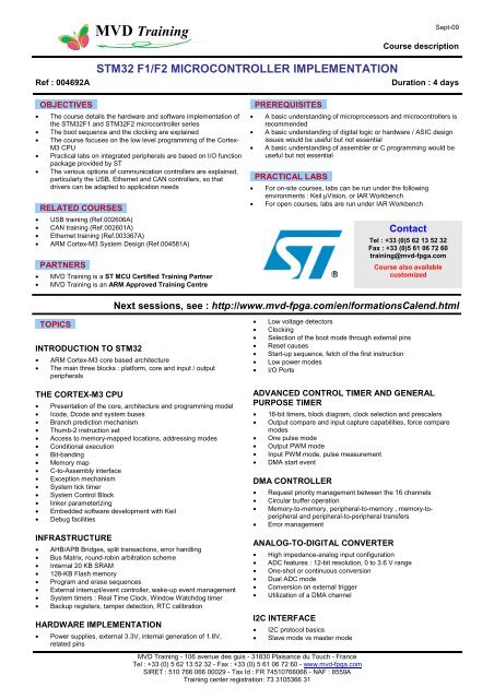
MVD TrainingSept-09Course descriptionRef : 004692A<strong>STM32</strong> F1/F2 MICROCONTROLLER IMPLEMENTATIONDuration : 4 daysOBJECTIVES• The course details the hardware and software implementation ofthe <strong>STM32</strong>F1 and <strong>STM32</strong>F2 microcontroller series• The boot sequence and the clocking are explained• The course focuses on the low level programming of the Cortex-M3 CPU• Practical labs on integrated peripherals are based on I/O functionpackage provided by ST• The various options of communication controllers are explained,particularly the USB, Ethernet and CAN controllers, so thatdrivers can be adapted to application needsRELATED COURSES• USB training (Ref.002606A)• CAN training (Ref.002601A)• Ethernet training (Ref.003367A)• ARM Cortex-M3 System Design (Ref.004581A)PARTNERS• MVD Training is a ST MCU Certified Training Partner• MVD Training is an ARM Approved Training CentrePREREQUISITES• A basic understanding of microprocessors and microcontrollers isrecommended• A basic understanding of digital logic or hardware / ASIC designissues would be useful but not essential• A basic understanding of assembler or C programming would beuseful but not essentialPRACTICAL LABS• For on-site courses, labs can be run under the followingenvironments : Keil µVision, or IAR Workbench• For open courses, labs are run under IAR WorkbenchContactTel : +33 (0)5 62 13 52 32Fax : +33 (0)5 61 06 72 60training@mvd-fpga.comCourse also availablecustomizedNext sessions, see : http://www.mvd-fpga.com/en/formationsCalend.htmlTOPICSINTRODUCTION TO <strong>STM32</strong>• ARM Cortex-M3 core based architecture• The main three blocks : platform, core and input / outputperipheralsTHE CORTEX-M3 CPU• Presentation of the core, architecture and programming model• Icode, Dcode and system buses• Branch prediction mechanism• Thumb-2 instruction set• Access to memory-mapped locations, addressing modes• Conditional execution• Bit-banding• Memory map• C-to-Assembly interface• Exception mechanism• System tick timer• System Control Block• linker parameterizing• Embedded software development with Keil• Debug facilitiesINFRASTRUCTURE• AHB/APB Bridges, split transactions, error handling• Bus Matrix, round-robin arbitration scheme• Internal 20 KB SRAM• 128-KB Flash memory• Program and erase sequences• External interrupt/event controller, wake-up event management• System timers : Real Time Clock, Window Watchdog timer• Backup registers, tamper detection, RTC calibrationHARDWARE IMPLEMENTATION• Power supplies, external 3.3V, internal generation of 1.8V,related pins• Low voltage detectors• Clocking• Selection of the boot mode through external pins• Reset causes• Start-up sequence, fetch of the first instruction• Low power modes• I/O PortsADVANCED CONTROL TIMER AND GENERALPURPOSE TIMER• 16-bit timers, block diagram, clock selection and prescalers• Output compare and input capture capabilities, force comparemodes• One pulse mode• Output PWM mode• Input PWM mode, pulse measurement• DMA start eventDMA CONTROLLER• Request priority management between the 16 channels• Circular buffer operation• Memory-to-memory, peripheral-to-memory , memory-toperipheraland peripheral-to-peripheral transfers• Error managementANALOG-TO-DIGITAL CONVERTER• High impedance-analog input configuration• ADC features : 12-bit resolution, 0 to 3.6 V range• One-shot or continuous conversion• Dual ADC mode• Conversion on external trigger• Utilization of a DMA channelI2C INTERFACE• I2C protocol basics• Slave mode vs master modeMVD Training - 106 avenue des guis - 31830 Plaisance du Touch - FranceTel : +33 (0) 5 62 13 52 32 - Fax : +33 (0) 5 61 06 72 60 - www.mvd-fpga.comSIRET : 510 766 066 00029 - Tax Id : FR 74510766066 - NAF : 8559ATraining center registration: 73 3105366 31
MVD Training• Transmit and receive sequencesSERIAL PERIPHERAL INTERFACE [SPI]• SPI protocol basics• Queue mode operation• Transfer sequenceUSART• Queue operation mode• Hardware flow control• Transmit and receive sequences• LIN mode• Smartcard interfaceCAN• CAN protocol basics• CAN controller organization• Filtering of received messages, acceptance filters• FIFO mode management• Test modes : loop back / silent modes• Configuring the bit timingUSB OTG FULL SPEED INTERFACE• USB protocol basics• Buffer description block, buffer descriptor table• DMA controller used to move data between buffers andEndPoints• Endpoint initialisation• Suspend / resume eventsSept-09Course descriptionFLEXIBLE STATIC MEMORY CONTROLLER• NOR / PSRAM interface• NAND / PC CARD interface• Memory bank mapping• Address mapping and chip select signals• LCD module interfaceETHERNET MAC• Automatic CRC• Flow control• DMA transfers• Address filtering• IEEE 1588 PTP• MII interface• RMON/MIB• LAN Wakeup frames / Magic packet• VLAN tagsDIGITAL-TO-ANALOG CONVERTER• DAC implementation• DMA capability• External triggersSDIO• Compliance• Implementation• DMA requestsDOCUMENTATIONTraining manuals will be given to attendees during training in print.MVD Training - 106 avenue des guis - 31830 Plaisance du Touch - FranceTel : +33 (0) 5 62 13 52 32 - Fax : +33 (0) 5 61 06 72 60 - www.mvd-fpga.comSIRET : 510 766 066 00029 - Tax Id : FR 74510766066 - NAF : 8559ATraining center registration: 73 3105366 31