MAX9157 Quad Bus LVDS Transceiver - Maxim
MAX9157 Quad Bus LVDS Transceiver - Maxim
MAX9157 Quad Bus LVDS Transceiver - Maxim

Create successful ePaper yourself
Turn your PDF publications into a flip-book with our unique Google optimized e-Paper software.
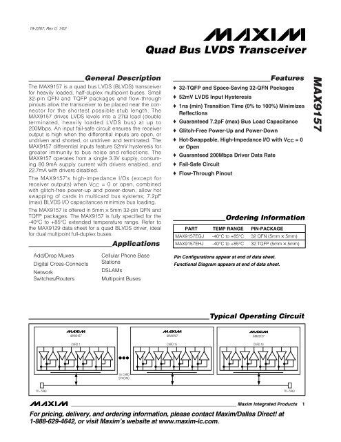
19-2287; Rev 0; 1/02<strong>Quad</strong> <strong>Bus</strong> <strong>LVDS</strong> <strong>Transceiver</strong>General DescriptionThe <strong>MAX9157</strong> is a quad bus <strong>LVDS</strong> (B<strong>LVDS</strong>) transceiverfor heavily loaded, half-duplex multipoint buses. Small32-pin QFN and TQFP packages and flow-throughpinouts allow the transceiver to be placed near the connectorfor the shortest possible stub length. The<strong>MAX9157</strong> drives <strong>LVDS</strong> levels into a 27Ω load (doubleterminated, heavily loaded <strong>LVDS</strong> bus) at up to200Mbps. An input fail-safe circuit ensures the receiveroutput is high when the differential inputs are open, orundriven and shorted, or undriven and terminated. The<strong>MAX9157</strong> differential inputs feature 52mV hysteresis forgreater immunity to bus noise and reflections. The<strong>MAX9157</strong> operates from a single 3.3V supply, consuming80.9mA supply current with drivers enabled, and22.7mA with drivers disabled.The <strong>MAX9157</strong>’s high-impedance I/Os (except forreceiver outputs) when V CC = 0 or open, combinedwith glitch-free power-up and power-down, allow hotswapping of cards in multicard bus systems; 7.2pF(max) B<strong>LVDS</strong> I/O capacitances minimize bus loading.The <strong>MAX9157</strong> is offered in 5mm ✕ 5mm 32-pin QFN andTQFP packages. The <strong>MAX9157</strong> is fully specified for the-40°C to +85°C extended temperature range. Refer tothe MAX9129 data sheet for a quad B<strong>LVDS</strong> driver, idealfor dual multipoint full-duplex buses.ApplicationsFeatures♦ 32-TQFP and Space-Saving 32-QFN Packages♦ 52mV <strong>LVDS</strong> Input Hysteresis♦ 1ns (min) Transition Time (0% to 100%) MinimizesReflections♦ Guaranteed 7.2pF (max) <strong>Bus</strong> Load Capacitance♦ Glitch-Free Power-Up and Power-Down♦ Hot-Swappable, High-Impedance I/O with V CC = 0or Open♦ Guaranteed 200Mbps Driver Data Rate♦ Fail-Safe Circuit♦ Flow-Through PinoutOrdering InformationPART TEMP RANGE PIN-PACKAGE<strong>MAX9157</strong>EGJ -40°C to +85°C 32 QFN (5mm ✕ 5mm)<strong>MAX9157</strong>EHJ -40°C to +85°C 32 TQFP (5mm ✕ 5mm)<strong>MAX9157</strong>Add/Drop MuxesDigital Cross-ConnectsNetworkSwitches/RoutersCellular Phone BaseStationsDSLAMsMultipoint <strong>Bus</strong>esPin Configurations appear at end of data sheet.Functional Diagram appears at end of data sheet.Typical Operating Circuit<strong>MAX9157</strong> <strong>MAX9157</strong> <strong>MAX9157</strong>CARD 1 CARD 15 CARD 161in CARDSPACINGRt = 54ΩRt = 54Ω________________________________________________________________ <strong>Maxim</strong> Integrated Products 1For pricing, delivery, and ordering information, please contact <strong>Maxim</strong>/Dallas Direct! at1-888-629-4642, or visit <strong>Maxim</strong>’s website at www.maxim-ic.com.
<strong>Quad</strong> <strong>Bus</strong> <strong>LVDS</strong> <strong>Transceiver</strong><strong>MAX9157</strong>ABSOLUTE MAXIMUM RATINGSV CC , AV CC to GND................................................-0.3V to +4.0VDO_+/RIN_+, DO_-/RIN_-, to GND .......................-0.3V to +4.0VDIN_, DE_, RE_ to GND.........................................-0.3V to +4.0VRO_ to GND................................................-0.3V to (V CC + 0.3V)AGND to GND .......................................................-0.3V to +0.3VShort-Circuit Duration (DO_+/RIN_+, DO_-/RIN_-) ....ContinuousContinuous Power Dissipation (T A = +70°C)<strong>MAX9157</strong>EGJ (derate 21.2mW/°C above +70°C) .....1702mW<strong>MAX9157</strong>EHJ (derate 11.1mW/°C above +70°C).........889mWStorage Temperature Range .............................-65°C to +150°C<strong>Maxim</strong>um Junction Temperature .....................................+150°COperating Temperature Range ...........................-40°C to +85°CESD ProtectionHuman Body Model (DO_+/RIN_+, DO_-/RIN_-).............±4kVLead Temperature (soldering, 10s) .................................+300°CStresses beyond those listed under “Absolute <strong>Maxim</strong>um Ratings” may cause permanent damage to the device. These are stress ratings only, and functionaloperation of the device at these or any other conditions beyond those indicated in the operational sections of the specifications is not implied. Exposure toabsolute maximum rating conditions for extended periods may affect device reliability.DC ELECTRICAL CHARACTERISTICS(V CC = 3.0V to 3.6V, R L = 27Ω ±1%, differential input voltage |V ID | = 0.1V to V CC , input common-mode voltage V CM = 0.05V to 2.4V,input voltage range = 0 to V CC , DE_ = high, RE_ = low, T A = -40°C to +85°C, unless otherwise noted. Typical values are at V CC =3.3V, |V ID | = 0.2V, V CM = 1.2V, and T A = +25°C.) (Notes 1 and 2)PARAMETER SYMBOL CONDITIONS MIN TYP MAX UNITSB<strong>LVDS</strong> (DO_+/RIN_+, DO_-/RIN_-)Differential Input High Threshold V TH DE_ = low 26 100 mVDifferential Input Low Threshold V TL DE_ = low -100 -26 mVThreshold Hysteresis (Note 3) V HYST DE_ = lowT A = +25°C, V CC = 3.3V,V CM = 1.2V12 26 43Full operating range 9 26 780.1V ≤⏐VID⏐≤ 0.6V, DE_ = low -15 ±1.8 15 µAInput Current I IN+ , I IN-0.6V
<strong>Quad</strong> <strong>Bus</strong> <strong>LVDS</strong> <strong>Transceiver</strong>DC ELECTRICAL CHARACTERISTICS (continued)(V CC = 3.0V to 3.6V, R L = 27Ω ±1%, differential input voltage |V ID | = 0.1V to V CC , input common-mode voltage V CM = 0.05V to 2.4V,input voltage range = 0 to V CC , DE_ = high, RE_ = low, T A = -40°C to +85°C, unless otherwise noted. Typical values are at V CC =3.3V, |V ID | = 0.2V, V CM = 1.2V, and T A = +25°C.) (Notes 1 and 2)PARAMETER SYMBOL CONDITIONS MIN TYP MAX UNITSDifferential Output Short-CircuitCurrent (Note 3)Capacitance at <strong>Bus</strong> Pins(Note 3)LVCMOS/LVTTL OUTPUTS (RO_)I OSD DIN_ = high or low, V OD = 0 14.8 30 mAC OUTPUTCapacitance from DO_+/RIN_+ orDO_-/RIN_- to GND, V CC = 3.6V or 07.2 pF<strong>MAX9157</strong>Output High Voltage V OHI OH = -4.0mA,DE_ = lowOpen, undriven short, orundriven 27Ω parallelterminationVID = 100mVV CC -0.3V CC -0.3V CC -0.172V CC -0.172Output Low Voltage V OL I OL = 4.0mA, V ID = -100mV, DE_ = low 0.179 0.25 VVID = 100mV, V RO_ = V CC - 1.0V, DE_ = low -15 -22.7 mADynamic Output Current I ODVID = -100mV, V RO_ = 1.0V, DE_ = low 12 19.9 mAVOutput Short-Circuit Current(Note 4)I OS VID = 100mV, V RO_ = 0, DE_ = low -52 -130 mAOutput High-Impedance Current I OZ RE_ = high, V RO = 0 or V CC -10 0.1 +10 µACapacitance at Receiver Output(Note 3)LVCMOS/LVTTL INPUTS (DIN, DE, RE)C OUTPUTCapacitance from RO_ to GND, V CC = 3.6Vor 04.5 pFInput High Voltage V IH 2.0 1.825 V CC VInput Low Voltage V IL GND 1.315 0.8 VInput Current I IN V DE_ , V RE_ , V DIN_ = high or low -20 ±9.2 20 µAPower-Off Input Current I INOV DE_ , V RE_ , V DIN_ = 3.6V or 0, V CC = 0or openSUPPLYSupply Current Drivers andReceivers Enabled-20 ±2.4 20 µAI CC DE_ = high, RE_ = low, R L = 27Ω 80.9 95 mASupply Current Drivers Enabledand Receivers DisabledSupply Current Drivers Disabledand Receivers EnabledSupply Current Drivers Disabledand Receivers DisabledI CCD DE_ = high, RE_ = high, R L = 27Ω 80.9 95 mAI CCR DE_ = low, RE_ = low 22.7 30 mAI CCZ DE_ = low, RE_ = high 22.7 30 mA_______________________________________________________________________________________ 3
<strong>Quad</strong> <strong>Bus</strong> <strong>LVDS</strong> <strong>Transceiver</strong><strong>MAX9157</strong>AC ELECTRICAL CHARACTERISTICS(V CC = 3.0V to 3.6V, R L = 27Ω ±1%, differential input voltage |V ID | = 0.2V to V CC , input frequency to <strong>LVDS</strong> inputs = 85MHz, input frequencyto LVCMOS/LVTTL inputs = 100MHz, LVCMOS/LVTTL inputs = 0 to 3V with 2ns (10% to 90%) transition times. Differential inputvoltage transition time = 1ns (20% to 80%). Input common-mode voltage V CM = 1.2V to 1.8V, DE_ = high, RE_ = low, T A = -40°C to+85°C, unless otherwise noted. Typical values are at V CC = 3.3V, |V ID | = 0.2V, V CM = 1.2V, and T A = +25°C.) (Notes 3 and 5)DRIVERPARAMETER SYMBOL CONDITIONS MIN TYP MAX UNITSDifferential Propagation DelayHigh to LowDifferential Propagation DelayLow to Hight PHLDt PLHDRE_ = high, C L = 10pF, <strong>MAX9157</strong>EGJ 1.2 1.96 2.5Figures 3, 4 <strong>MAX9157</strong>EHJ 1.1 1.87 2.4RE_ = high, C L = 10pF, <strong>MAX9157</strong>EGJ 1.2 1.94 2.5Figures 3, 4 <strong>MAX9157</strong>EHJ 1.1 1.84 2.4nsnsDifferential Skew | t PHLD - t PLHD |(Note 6)Channel-to-Channel Skew(Note 7)t SKD1 RE_ = high, C L = 10pF, Figures 3, 4 33 160 pst CCSK RE_ = high, C L = 10pF, Figures 3, 4 58 300 psChip-to-Chip Skew (Note 8) t SKD2 RE_ = high, C L = 10pF, Figures 3, 4 0.38 0.8 nsChip-to-Chip Skew (Note 9) T SKD3 RE_ = high, C L = 10pF, Figures 3, 4 1.3 nsRE_ = high, C <strong>MAX9157</strong>EGJ 0.6 1.13 1.4Rise Time t L = 10pF,TLHFigures 3, 4 <strong>MAX9157</strong>EHJ 0.6 1.07 1.4RE_ = high, C <strong>MAX9157</strong>EGJ 0.6 1.16 1.4Fall Time t L = 10pF,THLFigures 3, 4 <strong>MAX9157</strong>EHJ 0.6 1.11 1.4RE_ = high, C <strong>MAX9157</strong>EGJ 6.79 8Disable Time High to Z t L = 10pF,PHZFigures 5, 6 <strong>MAX9157</strong>EHJ 6.79 8RE_ = high, C <strong>MAX9157</strong>EGJ 3.16 8Disable Time Low to Z t L = 10pF,PLZFigures 5, 6 <strong>MAX9157</strong>EHJ 3.48 8RE_ = high, C <strong>MAX9157</strong>EGJ 4.67 7Enable Time Z to High t L = 10pF,PZHFigures 5, 6 <strong>MAX9157</strong>EHJ 4.71 7RE_ = high, C <strong>MAX9157</strong>EGJ 4.36 7Enable Time Z to Low t L = 10pF,PZLFigures 5, 6 <strong>MAX9157</strong>EHJ 4.39 7nsnsnsnsnsns<strong>Maxim</strong>um Operating Frequency(Note 10)f MAX RE_ = high, C L = 10pF, Figures 5, 6 100 MHzRECEIVERDifferential Propagation DelayHigh to LowDifferential Propagation DelayLow to HighDE_ = low, Figures 7, 8; <strong>MAX9157</strong>EGJ 1.8 2.58 4.1t PHLDC L =15pF <strong>MAX9157</strong>EHJ 1.8 2.61 4.1DE_ = low, Figures 7, 8; <strong>MAX9157</strong>EGJ 1.8 2.49 4.1t PLHDC L =15pF <strong>MAX9157</strong>EHJ 1.8 2.52 4.1nsnsDifferential Skew | tPHLD -tPLHD | (Note 6)Channel-to-Channel Skew(Note 7)t SKD1 DE_ = low, Figures 7, 8; C L = 15pF 90 450 pst CCSK DE_ = low, Figures 7, 8; C L = 15pF 131 580 psChip-to-Chip Skew (Note 8) t SKD2 DE_ = low, Figures 7, 8; C L =15pF 0.7 1.7 nsChip-to-Chip Skew (Note 9) t SKD3 DE_ = low, Figures 7, 8; C L =15pF 0.7 1.7 nsRise Time t TLH DE_ = low, Figures 7, 8; C L = 15pF 0.5 1.1 1.6 ns4 _______________________________________________________________________________________
<strong>Quad</strong> <strong>Bus</strong> <strong>LVDS</strong> <strong>Transceiver</strong>AC ELECTRICAL CHARACTERISTICS (continued)(V CC = 3.0V to 3.6V, R L = 27Ω ±1%, differential input voltage |V ID | = 0.2V to V CC , input frequency to <strong>LVDS</strong> inputs = 85MHz, input frequencyto LVCMOS/LVTTL inputs = 100MHz, LVCMOS/LVTTL inputs = 0 to 3V with 2ns (10% to 90%) transition times. Differential inputvoltage transition time = 1ns (20% to 80%). Input common-mode voltage V CM = 1.2V to 1.8V, DE_ = high, RE_ = low, T A = -40°C to+85°C, unless otherwise noted. Typical values are at V CC = 3.3V, |V ID | = 0.2V, V CM = 1.2V, and T A = +25°C.) (Notes 3 and 5)PARAMETER SYMBOL CONDITIONS MIN TYP MAX UNITSFall Time t THL DE_ = low, Figures 7, 8; C L = 15pF 0.7 1.2 1.8 nsDE_ = low, R <strong>MAX9157</strong>EGJ 6.74 8Disable Time High to Z t L = 500Ω, C LPHZ= 15pF, Figures 9, 10 <strong>MAX9157</strong>EHJ 6.82 8DE_ = low, R <strong>MAX9157</strong>EGJ 6.49 8Disable Time Low to Z t L = 500Ω, C PLZ L= 15pF, Figures 9, 10 <strong>MAX9157</strong>EHJ 6.79 8DE_ = low, R <strong>MAX9157</strong>EGJ 4.67 7Enable Time Z to High t L = 500Ω, C PZH L= 15pF, Figures 9, 10 <strong>MAX9157</strong>EHJ 4.57 7DE_ = low, R <strong>MAX9157</strong>EGJ 5.43 7Enable Time Z to Low t L = 500Ω, C PZL L= 15pF, Figures 9, 10 <strong>MAX9157</strong>EHJ 4.71 7<strong>Maxim</strong>um Operating Frequency(Note 10)f MAX DE_ = low, C L= 15pF 85 MHzNote 1: Current into a pin is defined as positive. Current out of a pin is defined as negative. All voltages are referenced to groundexcept V TH , V TL , V ID , V HYST , V OD , and ∆V OD .Note 2: <strong>Maxim</strong>um and minimum limits over temperature are guaranteed by design and characterization. Devices are productiontested at T A = +25°C.Note 3: Guaranteed by design and characterization.Note 4: Short only one output at a time. Do not exceed the absolute maximum junction temperature specification.Note 5: C L includes scope probe and test jig capacitance.Note 6: t SKD1 is the magnitude difference of differential propagation delays in a channel. t SKD1 = | t PHLD - t PLHD |.Note 7: t CCSK is the magnitude difference of the t PLHD or t PHLD of one channel and the t PLHD or t PHLD of any other channel on thesame part.Note 8: t SKD2 is the magnitude difference of any differential propagation delays between parts operating over rated conditions atthe same V CC and within 5°C of each other.Note 9: t SKD3 is the magnitude difference of any differential propagation delays between parts operating over rated conditions.Note 10: Meets data sheet specifications while operating at minimum f MAX rating.Typical Operating Characteristics(V CC = 3.3V, R L = 27Ω, driver C L = 10pF, receiver C L = 15pF, |V ID | = 200mV, V CM = 1.2V, f IN = 20MHz, T A = +25°C, unless otherwise noted.)nsnsnsns<strong>MAX9157</strong>SUPPLY CURRENT (mA)10510095908580SUPPLY CURRENT vs. FREQUENCYFOUR CHANNELSDRIVENV CC = 3.6VV CC = 3.3VV CC = 3.0V<strong>MAX9157</strong> toc01DIFFERENTIAL OUTPUT VOLTAGE (V)0.4050.4040.4030.4020.401DIFFERENTIAL OUTPUT VOLTAGEvs. SUPPLY VOLTAGE<strong>MAX9157</strong> toc02DIFFERENTIAL OUTPUT VOLTAGE (V)2.01.81.61.41.21.00.80.60.40.2DIFFERENTIAL OUTPUT VOLTAGEvs. OUTPUT LOAD<strong>MAX9157</strong> toc03750.01 0.1 1 10 100 1000FREQUENCY (MHz)0.4003.0 3.1 3.2 3.3 3.4 3.5 3.6SUPPLY VOLTAGE (V)015 45 75 105 135OUTPUT LOAD (Ω)_______________________________________________________________________________________ 5
<strong>Quad</strong> <strong>Bus</strong> <strong>LVDS</strong> <strong>Transceiver</strong><strong>MAX9157</strong>Typical Operating Characteristics (continued)(V CC = 3.3V, R L = 27Ω, driver C L = 10pF, receiver C L = 15pF, |V ID | = 200mV, V CM = 1.2V, f IN = 20MHz, T A = +25°C, unless otherwise noted.)DRIVER TRANSITION TIME (ns)1.31.21.1DRIVER TRANSITION TIMEvs. LOAD CAPACITANCE<strong>MAX9157</strong> toc04DRIVER TRANSITION TIME (ns)t THLt TLH1.00.90.80.71.31.21.1DRIVER TRANSITION TIMEvs. TEMPERATUREt THLt TLH<strong>MAX9157</strong> toc051.05 10 15 20 25LOAD CAPACITANCE (pF)-40 -15 10 35 60 85TEMPERATURE (°C)DRIVER TRANSITION TIME (ns)1.201.151.101.051.000.95DRIVER TRANSITION TIMEvs. SUPPLY VOLTAGE<strong>MAX9157</strong> toc063.02.5t THL2.0t TLHRECEIVER TRANSITION TIME (ns)1.51.00.5RECEIVER TRANSITION TIMEvs. LOAD CAPACITANCEt THLt TLH<strong>MAX9157</strong> toc070.903.0 3.1 3.2 3.3 3.4 3.5 3.6SUPPLY VOLTAGE (V)05 10 15 20 25 30LOAD CAPACITANCE (pF)6 _______________________________________________________________________________________
<strong>Quad</strong> <strong>Bus</strong> <strong>LVDS</strong> <strong>Transceiver</strong>PIN NAME FUNCTION1, 2, 22, 23, 24 N.C. No Connection. Not internally connected.3 VCC Digital Power Supply4, 21 GND Digital Ground5 RE34Pin DescriptionReceiver Channels 3 and 4 Enable (Enable Low). Drive RE34 low to enable receiverchannels 3 and 4.6 DE34Driver Channels 3 and 4 Enable (Enable High). Drive DE34 high to enable driver channels3 and 4.7, 17 AGND Analog Ground8, 19 AV CC Analog Power Supply9 DO4-/RIN4- Channel 4 Inverting B<strong>LVDS</strong> Input/Output10 DO4+/RIN4+ Channel 4 Noninverting B<strong>LVDS</strong> Input/Output11 DO3-/RIN3- Channel 3 Inverting B<strong>LVDS</strong> Input/Output12 DO3+/RIN3+ Channel 3 Noninverting B<strong>LVDS</strong> Input/Output13 DO2-/RIN2- Channel 2 Inverting B<strong>LVDS</strong> Input/Output14 DO2+/RIN2+ Channel 2 Noninverting B<strong>LVDS</strong> Input/Output15 DO1-/RIN1- Channel 1 Inverting B<strong>LVDS</strong> Input/Output16 DO1+/RIN1+ Channel 1 Noninverting B<strong>LVDS</strong> Input/Output18 DE12Driver Channels 1 and 2 Enable (Enable High). Drive DE12 high to enable driver channels1 and 2.20 RE12Receiver Channels 1 and 2 Enable (Enable Low). Drive RE12 low to enable receiverchannels 1 and 2.25 DIN1 Driver Channel 1 Input26 RO1 Receiver Channel 1 Output27 DIN2 Driver Channel 2 Input28 RO2 Receiver Channel 2 Output29 DIN3 Driver Channel 3 Input30 RO3 Receiver Channel 3 Output31 DIN4 Driver Channel 4 Input32 RO4 Receiver Channel 4 OutputEP* EXPOSED PAD Exposed Pad. Solder exposed pad to GND.*<strong>MAX9157</strong>EGJ only.<strong>MAX9157</strong>_______________________________________________________________________________________ 7
<strong>Quad</strong> <strong>Bus</strong> <strong>LVDS</strong> <strong>Transceiver</strong><strong>MAX9157</strong>Detailed DescriptionThe <strong>MAX9157</strong> is a four-channel, 200Mbps, 3.3V B<strong>LVDS</strong>transceiver in 32-lead TQFP and QFN packages, idealfor driving heavily loaded multipoint buses, typically 16to 20 cards plugged into a backplane. The <strong>MAX9157</strong>receivers accept a differential input and have a fail-safeinput circuit. The devices detect differential signals aslow as 100mV and as high as V CC .The <strong>MAX9157</strong> driver outputs use a current-steeringconfiguration to generate a 9.25mA to 17mA outputcurrent. This current-steering approach induces lessground bounce and no shoot-through current, enhancingnoise margin and system speed performance. Theoutputs are short-circuit current limited.The <strong>MAX9157</strong> current-steering output requires a resistiveload to terminate the signal and complete the transmissionloop. Because the devices switch the directionof current flow and not voltage levels, the output voltageswing is determined by the value of the terminationresistor multiplied by the output current. With a typical15mA output current, the <strong>MAX9157</strong> produces a 405mVoutput voltage when driving a bus terminated with two54Ω resistors (15mA ✕ 27Ω = 405mV). Logic states aredetermined by the direction of current flow through thetermination resistor.Fail-Safe Receiver InputsThe fail-safe feature of the <strong>MAX9157</strong> sets the outputhigh when the differential input is:• Open• Undriven and shorted• Undriven and terminatedWithout a fail-safe circuit, when the input is undriven,noise at the input may switch the outputs and it mayappear to the system that data is being sent. Open orundriven terminated input conditions can occur when acable is disconnected or cut, or when driver output is inhigh impedance. A shorted input can occur because ofa cable failure.When the input is driven with a differential signal with acommon-mode voltage of 0.05V to 2.4V, the fail-safecircuit is not activated. If the input is open, undrivenand shorted, or undriven and parallel terminated, aninternal resistor in the fail-safe circuit pulls both inputsabove V CC - 0.3V, activating the fail-safe circuit andforcing the outputs high (Figure 1).Effect of Capacitive LoadingThe characteristic impedance of a differential PC boardtrace is uniformly reduced when equal capacitive loadsare attached at equal intervals (provided the transitiontime of the signal being driven on the trace is longerthan the delay between loads). This kind of loading istypical of multipoint buses where cards are attached at1in or 0.8in intervals along the length of a backplane.The reduction in characteristic impedance is approximatedby the following formula:Z DIFF -loaded = Z DIFF -unloaded ✕SQRT [Co / (Co + N ✕ C L / L)]where:Z DIFF -unloaded = unloaded differential characteristicimpedanceCo = unloaded trace capacitance (pF/unit length)C L = value of each capacitive load (pF)N = number of capacitive loadsL = trace lengthFor example, if Co = 2.5pF/in, C L = 10pF, N = 18, L =18in, and Z DIFF -unloaded = 120Ω, the loaded differentialimpedance is:Z DIFF -loaded = 120Ω ✕SQRT [2.5pF / (2.5pF + 18 x 10pF / 18in)]ZDIFF-loaded = 54ΩIn this example, capacitive loading reduces the characteristicimpedance from 120Ω to 54Ω. The load seen byDO_+/RIN_+D0_-/RIN_-R IN1R IN1R IN2V CCV CC - 0.3V<strong>MAX9157</strong>RO_Figure 1. Internal Fail-Safe Circuit8 _______________________________________________________________________________________
<strong>Quad</strong> <strong>Bus</strong> <strong>LVDS</strong> <strong>Transceiver</strong>a driver located on a card in the middle of the bus is27Ω because the driver sees two 54Ω loads in parallel.A typical <strong>LVDS</strong> driver (rated for a 100Ω load) would notdevelop a large enough differential signal to be reliablydetected by an <strong>LVDS</strong> receiver. The <strong>MAX9157</strong> B<strong>LVDS</strong>drivers are designed and specified to drive a 27Ω loadto differential voltage levels of 250mV to 460mV. A standard<strong>LVDS</strong> receiver is able to detect this level of differentialsignal. Short extensions off the bus, called stubs,contribute to capacitive loading. Keep stubs less than1in for a good balance between ease of componentplacement and good signal integrity.The <strong>MAX9157</strong> driver outputs are current-source driversand drive larger differential signal levels into loadslighter than 27Ω and smaller levels into loads heavierthan 27Ω (see Typical Operating Characteristicscurves). To keep loading from reducing bus impedancebelow the rated 27Ω load, PC board traces can bedesigned for higher unloaded characteristic impedance.Effect of Transition TimesFor transition times (measured from 0% to 100%) shorterthan the delay between capacitive loads, the loadsare seen as low-impedance discontinuities from whichthe driven signal is reflected. Reflections add and subtractfrom the signal being driven and cause decreasednoise margin and jitter. The <strong>MAX9157</strong> output driversare designed for a minimum transition time of 1ns(rated 0.6ns from 20% to 80%, or about 1ns from 0% to100%) to reduce reflections while being fast enough forhigh-speed backplane data transmission.Power-On ResetThe power-on reset voltage of the <strong>MAX9157</strong> is typically2.25V. When the supply falls below this voltage, thedevices are disabled and the receiver inputs/driver outputsare in high impedance. The power-on resetensures glitch-free power-up and power-down, allowinghot swapping of cards in a multicard bus systemwithout disrupting communications.Receiver Input HysteresisThe <strong>MAX9157</strong> receiver inputs feature 52mV hysteresis toincrease noise immunity for low-differential input signals.Operating ModesThe <strong>MAX9157</strong> features driver/receiver enable inputsthat select the bus I/O function (Table 1). Tables 2 and3 show the driver and receiver truth tables.Input Internal Pullup/PulldownResistorsThe <strong>MAX9157</strong> includes pullup or pulldown resistors(300kΩ) to ensure that unconnected inputs are defined(Table 4).Applications InformationSupply BypassingBypass each supply pin with high-frequency surfacemountceramic 0.1µF and 1nF capacitors in parallel asclose to the device as possible, with the smaller valuecapacitor closest to the device.TerminationIn the example given in the Effect of Capacitive Loadingsection, the loaded differential impedance of a bus isreduced to 54Ω. Since the bus can be driven from anycard position, the bus must be terminated at each end. Aparallel termination of 54Ω at each end of the bus placedacross the traces that make up the differential pair providesa proper termination. The total load seen by the driveris 27Ω. The <strong>MAX9157</strong> drives higher differential signallevels into lighter loads. (See Differential Output Voltagevs. Output Load graph in the Typical Operating Characteristicssection). A multidrop bus with the driver at oneend and receivers connected at regular intervals alongthe bus has a lowered impedance due to capacitive loading.Assuming a 54Ω impedance, the multidrop bus canbe terminated with a single, parallel-connected 54Ω resistorat the far end from the driver. Only a single resistor isrequired because the driver sees one 54Ω differentialtrace. The signal swing is larger with a 54Ω load. In general,parallel terminate each end of the bus with a resistorTable 1. I/O Enable Functional TableMODE SELECTED DE_ RE_Driver Mode H HReceiver Mode L LHigh-Impedance Mode L HLoopback Mode H LTable 2. Driver ModeINPUTSOUTPUTSDE_ DIN_ DO_+/RIN_+ DO_-/RIN_-H L L HH H H LL X Z Z<strong>MAX9157</strong>_______________________________________________________________________________________ 9
<strong>Quad</strong> <strong>Bus</strong> <strong>LVDS</strong> <strong>Transceiver</strong><strong>MAX9157</strong>Table 3. Receiver ModeINPUTSOUTPUTSRE_ V ID = (V DO_+ /R IN_+ ) - (V DO_- /R IN_- ) RO_L V ID < -100mV LL V ID > 100mV HLFail-safe operation guaranteed whenDO_+/RIN_+ and DO_-/RIN_- areopen, undriven and shorted, orundriven and parallel terminatedH X ZHAvoid the use of unbalanced cables, such as ribboncable. Balanced cables, such as twisted pair, offersuperior signal quality and tend to generate less EMIdue to canceling effects. Balanced cables tend to pickup noise as common mode, which is rejected by thereceiver.Board LayoutA four-layer PC board that provides separate power,ground, input, and output signals is recommended.Keep the LVTTL/LVCMOS and B<strong>LVDS</strong> signals separatedto prevent coupling.Table 4. Input Internal Pullup/PulldownResistorsD0_+/RIN_+PININTERNAL RESISTORDE12DE34RE12RE34Pulldown to GNDPulldown to GNDPullup to V CCPullup to V CCV CCGNDDIN_R L /2R L /2V OSV ODV OSDIN_Pullup to V CCDO_-/RIN_-matching the differential impedance of the bus (takinginto account any reduced impedance due to loading).Traces, Cables, and ConnectorsThe characteristics of input and output connectionsaffect the performance of the <strong>MAX9157</strong>. Use controlled-impedancetraces, cables, and connectors withmatched characteristic impedance.Ensure that noise couples as common mode by runningthe traces of a differential pair close together.Reduce within-pair skew by matching the electricallength of the traces of a differential pair. Excessiveskew can result in a degradation of magnetic field cancellation.Maintain the distance between traces of a differentialpair to avoid discontinuities in differentialimpedance. Minimize the number of vias to further preventimpedance discontinuities.Figure 2. Driver V OD and V OS Test CircuitC LDO_+/RIN_+DIN_GENERATORR L50ΩDO_-/RIN_-C LFigure 3. Driver Propagation Delay and Transition Time Test Circuit10 ______________________________________________________________________________________
<strong>Quad</strong> <strong>Bus</strong> <strong>LVDS</strong> <strong>Transceiver</strong>50%t PLHD20%t TLHV CC50%0t PHLDV OH0 DIFFERENTIAL0V OL80%80%00V OD = (V DO_+/RIN_+ - V DO_-/RIN_-)20%t THLGENERATORV CCGND50ΩDIN_DE_1/4 <strong>MAX9157</strong>C LR L /2R L /2C LDO_+/RIN_++1.2VDIN_RIN_-RIN_+V ODDO_-/RIN_-<strong>MAX9157</strong>Figure 4. Driver Propagation Delay and Transition TimeWaveformsFigure 5. Driver High-Impedance Delay Test CircuitDE_V CC50%50%0D0_+/RIN_+ WHEN DIN_ = V CCDO_-/RIN_- WHEN DIN_ = 0t PHZ50%t PZH50%V OH1.2V1.2VDO_+/RIN_+ WHEN DIN_ = 0DO_-/RIN_- WHEN DIN_ = V CCt PLZ50%t PZL50%V OLFigure 6. Driver High-Impedance Delay WaveformDO_+/RIN_+PULSEGENERATORDO_-/RIN_-C LRO_50Ω* 50Ω*RECEIVER ENABLED1/4 <strong>MAX9157</strong>*50Ω REQUIRED FOR PULSE GENERATOR TERMINATION.Figure 7. Receiver Transition Time and Propagation Delay Test Circuit______________________________________________________________________________________ 11
<strong>Quad</strong> <strong>Bus</strong> <strong>LVDS</strong> <strong>Transceiver</strong><strong>MAX9157</strong>DO_-/RIN_-DO_+/RIN_+t PLHDV IDV CM V CM50%80% 80%t PHLDV OH50%20%20%RO_t TLHt THLV OLFigure 8. Receiver Transition Time and Propagation Delay Timing DiagramV CCS 1GENERATORDO_+/RIN_+DO_-/RIN_-RE_R LC LRO_50Ω1/4 <strong>MAX9157</strong>C L INCLUDES LOAD AND TEST JIG CAPACITANCE.S 1 = V CC FOR t PZL AND t PLZ MEASUREMENTS.S 1 = GND FOR t PZH AND t PHZ MEASUREMENTS.Figure 9. Receiver High-Impedance Delay Test CircuitV CC50%50%RE_0t PZLt PLZ50%V CCRO_ WHENV ID = -100mVRO_ WHENV ID = +100mVt PHZ0.5V0.5Vt PZH50%V OLV OHGNDFigure 10. Receiver High-Impedance Waveforms12 ______________________________________________________________________________________
<strong>Quad</strong> <strong>Bus</strong> <strong>LVDS</strong> <strong>Transceiver</strong>DIN1DE12RO1RE12Functional DiagramDO1+/RIN1+DO1-/RIN1-TOP VIEWN.C. 1N.C. 2Pin ConfigurationsRO4DIN4RO3DIN3RO2DIN2RO1DIN132 31 30 29 28 27 26 2524 N.C.23 N.C.<strong>MAX9157</strong>DO2+/RIN2+V CC322N.C.DIN2DO2-/RIN2-GNDRE3445<strong>MAX9157</strong>2120GNDRE12RO2DE34619AV CCAGND718DE12DIN3DO3+/RIN3+AV CC817AGNDDE34DO3-/RIN3-910 11 12 13 14 15 16RO3RE34DO4+/RIN4+DO3+/RIN3+DO2+/RIN2+DO4-/RIN4-DO3-/RIN3-DO2-/RIN2-DO1-/RIN1-DO1+/RIN1+DIN4DO4+/RIN4+TQFPDO4-/RIN4-RO4TOP VIEW3231302928272625N.C.1 24N.C.223V CC322GND421RE34DE34AGND567201918AV CC817DO4+/RIN4+DO3+/RIN3+DO2+/RIN2+DO4-/RIN4-DO3-/RIN3-DO2-/RIN2-DO1-/RIN1-DO1+/RIN1+910111213141516RO4DIN4RO3DIN3RO2DIN2RO1DIN1<strong>MAX9157</strong>N.C.N.C.N.C.GNDChip InformationTRANSISTOR COUNT: 1826<strong>MAX9157</strong>RE12AV CCDE12PROCESS: CMOSAGNDQFN______________________________________________________________________________________ 13
<strong>Quad</strong> <strong>Bus</strong> <strong>LVDS</strong> <strong>Transceiver</strong><strong>MAX9157</strong>Package Information14 ______________________________________________________________________________________
<strong>Quad</strong> <strong>Bus</strong> <strong>LVDS</strong> <strong>Transceiver</strong>Package Information (continued)<strong>MAX9157</strong>______________________________________________________________________________________ 15
<strong>Quad</strong> <strong>Bus</strong> <strong>LVDS</strong> <strong>Transceiver</strong><strong>MAX9157</strong>Package Information (continued)32L TQFP, 5x5x01.0.EPS<strong>Maxim</strong> cannot assume responsibility for use of any circuitry other than circuitry entirely embodied in a <strong>Maxim</strong> product. No circuit patent licenses areimplied. <strong>Maxim</strong> reserves the right to change the circuitry and specifications without notice at any time.<strong>Maxim</strong> Integrated Products, 120 San Gabriel Drive, Sunnyvale, CA 94086 408-737-7600 ____________________ 16© 2002 <strong>Maxim</strong> Integrated Products Printed USA is a registered trademark of <strong>Maxim</strong> Integrated Products.