T035320240 - Channel Microelectronic GmbH
T035320240 - Channel Microelectronic GmbH
T035320240 - Channel Microelectronic GmbH

You also want an ePaper? Increase the reach of your titles
YUMPU automatically turns print PDFs into web optimized ePapers that Google loves.
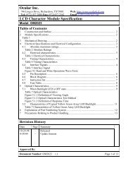
Ocular Inc.746 Lingco Drive, Richardson, TX75081 Web: http://www.ocularlcd.comTel: (972) 437-3888 Fax: (972)437-2562 Email: lcd@ocularlcd.comLCD Graphic TFT Module SpecificationModel: <strong>T035320240</strong>OSBFTable of Contents1 Construction and Outline..................................................................................................... 22 Module Specifications ........................................................................................................ 23 Electrical Specifications and Electrical Configuration........................................................ 33.1 Absolute maximum ratings.......................................................................................... 33.2 Electrical characteristics .............................................................................................. 33.3 Backlight Electrical Characteristic .............................................................................. 43.4 Interface Signals .......................................................................................................... 43.5 Block Diagrams ........................................................................................................... 63.5.1 System Block Diagram........................................................................................ 63.5.2 Source Driver whole Chip block diagram ........................................................... 63.5.3 Timing controller block diagram......................................................................... 73.5.4 Source Driver block diagram............................................................................... 73.5.5 Gate Driver block diagram .................................................................................. 84 Interface signal..................................................................................................................... 84.1 Timing Controller Timing Chart ................................................................................. 84.1.1 CCIR601 (HS_POL=”L” in Register R2) Clock and Data waveform ................ 84.1.2 Digital Serial RGB Clock and Data waveform.................................................... 94.1.3 Digital Parallel RGB Clock and Data waveform................................................. 94.1.4 FPC Input Data Mode.......................................................................................... 95 Optical Characteristics....................................................................................................... 106 Precautions Relating to Product Handling......................................................................... 127 Mechanical Drawing.......................................................................................................... 14Revision HistoryDate Page SummaryApproved By:Ocular <strong>T035320240</strong>OSBF draft specification Page 1 of 13
Ocular Inc.746 Lingco Drive, Richardson, TX75081 Web: http://www.ocularlcd.comTel: +1(972) 437 3888 Fax: +1(972) 437 2562 Email: lcd@ocularlcd.com1 Construction and OutlineConstruction:320 x 240 Dot Matrix TFT graphics moduleSource and Gate Driver: Himax HX8218 and HX8615 or approved equivalent.Outline:See Mechanical Drawing (Unit Outline Dimension).Interface signals: See section 3.4 interface signals.2 Module SpecificationsTable 1Parameter Specification UnitOutline dimensions 77.8(W)*64.5(H)*2.6max(D) mmDisplay format 320*RGB*240 pixels –Active Area 70.08(W)*52.56(H) mmDisplay ModeTransmissive Color Active Matrix LCDDiagonal dimension 3.5 inchDot Pitch 0.73(W)*0.219(H) mmPixel Pitch 0.219(W)*0.219(H) mmViewing Direction6 O’ClockBack light Color* White LED –Drive Configuration Himax HX8218A and HX8615A orcompatible DriverWeight TBD gOperating Temperature 0~60Storage Temperature -10 ~ 70o Co C3Ocular <strong>T035320240</strong>OSBF Module draft Specification Page 2 of 14
Ocular Inc.746 Lingco Drive, Richardson, TX75081 Web: http://www.ocularlcd.comTel: +1(972) 437 3888 Fax: +1(972) 437 2562 Email: lcd@ocularlcd.comElectrical Specifications and Electrical ConfigurationThe <strong>T035320240</strong>OSBF module utilizes the HX8218A and HX8615A source/gate driver. Thisdriver support a number of different interface options including Digital 8 bit Serial, 24 bitparallel RGB, CCIR601/656 and Digital Control timing. For detail interface and optionsselection, users are referred to the HX8218A and HX8615A specification.3.1 Absolute maximum ratingsTable 2Parameter Symbol Min. Max. Unit RemarkHumidity Hp 0 90 % RH Ta
Ocular Inc.746 Lingco Drive, Richardson, TX75081 Web: http://www.ocularlcd.comTel: +1(972) 437 3888 Fax: +1(972) 437 2562 Email: lcd@ocularlcd.com3.3 Backlight Electrical CharacteristicItem Symbol Conditions Min. Type Max. UnitForward Voltage Vf If=20.2mA 9.0 10.2 10.8 VForward Current If 20.2Power dissipation Pd If = 20.2mA .384 WAverage Brightness(without LCD)If If=20.2mA 2800 Cd/m2Color CoordinatesX=0.27~0.32,Y=0.27~0.323.4 Interface SignalsTable 4Pin#SymbolInput/OutputDescription1 A1 I Anode connection to backlight LED2 A2 I Anode connection to backlight LED3 K2 I Cathode connection to backlight LED4 K1 I Cathode connection to backlight LED5 GVSS I Gate driver voltage low normally digital ground6 GVDD I Gate driver voltage high normally 3.3 volt7 VGL I TFT gate operating voltage low typically -10 volt8 VGH I TFT gate operating voltage high normally 15 volt9 VCOM ITFT common Electrode voltage adjusted to optimize display quality: contrast ratio,cross talk etc.10 GND Digital ground.11 RESETB I Hardware global reset. Low active. Normally pull high.12 UD IUp/down scan setting.When UD=”H”, reverse scan.When UD=”L”, normal scan.13 LRC IThe shift direction of device internal shift register is controlled by this pin asshown below:LRC=H: STH->OUT1->• • •->OUT960->STHOLRC=L: STH->OUT960->• • •->OUT1->STHOControl the input data format.14 IF2IF2, IF1 Input data formatI L, L (default) Serial RGBL, H Parallel RGB15 IF1H, L CCIR601H, H CCIR65616 SPENA I Serial port Data Enable Signal. Normally pull high.17 SPCK I Serial port Clock. Normally pull high.18 SPDA I/O Serial port Data input/output.Ocular <strong>T035320240</strong>OSBF Module draft Specification Page 4 of 14
Ocular Inc.746 Lingco Drive, Richardson, TX75081 Web: http://www.ocularlcd.comTel: +1(972) 437 3888 Fax: +1(972) 437 2562 Email: lcd@ocularlcd.com19 D2720 D2621 D2522 D2423 D2324 D2225 D2126 D2027 D1728 D1629 D1530 D1431 D1332 D1233 D11IDigital data input. DX0 is LSB and DX7 is MSB.1. If parallel RGB input mode is used, D0X, D1X, and D2X indicate R, G,and B data in turn.2. If serial RGB or CCIR601/656 input mode is selected, only D07~D00 areused, and others short to GND.34 D1035 VDD I Analog power. 4.5V ~ 5.5V.36 VSS I Analog ground.37 D0738 D0639 D05Digital data input. DX0 is LSB and DX7 is MSB.1. If parallel RGB input mode is used, D0X, D1X, and D2X indicate R, G,40 D04and B data in turn.I41 D032. If serial RGB or CCIR601/656 input mode is selected, only D07~D00 areused, and others short to GND.42 D0243 D0144 D0045 CLK I Clock signal. Latching data at the rising edge.46 IHS I Horizontal sync input in digital RGB mode. Or HREF input in CCIR601mode. (Short to GND if not used)47 IVS I Vertical sync input in digital RGB mode. Or V123 input in CCIR601 mode.(Short to GND if not used)48 DEN I Input data enable control. Normally pull low.49 STB I Standby mode control. Normally pull high.When STB=”L”, source driver and DAC are off. All outputs are shorted toVSS.When STB=”H”, source driver and DAC are on.50 VCC I Digital power. 3V ~ 3.6V.Ocular <strong>T035320240</strong>OSBF Module draft Specification Page 5 of 14
Ocular Inc.746 Lingco Drive, Richardson, TX75081 Web: http://www.ocularlcd.comTel: +1(972) 437 3888 Fax: +1(972) 437 2562 Email: lcd@ocularlcd.com3.5 Block Diagrams3.5.1 System Block Diagram3.5.2 Source Driver whole Chip block diagramOcular <strong>T035320240</strong>OSBF Module draft Specification Page 6 of 14
Ocular Inc.746 Lingco Drive, Richardson, TX75081 Web: http://www.ocularlcd.comTel: +1(972) 437 3888 Fax: +1(972) 437 2562 Email: lcd@ocularlcd.com3.5.3 Timing controller block diagram3.5.4 Source Driver block diagramOcular <strong>T035320240</strong>OSBF Module draft Specification Page 7 of 14
Ocular Inc.746 Lingco Drive, Richardson, TX75081 Web: http://www.ocularlcd.comTel: +1(972) 437 3888 Fax: +1(972) 437 2562 Email: lcd@ocularlcd.com3.5.5 Gate Driver block diagram4 Interface signal4.1 Timing Controller Timing Chart4.1.1 CCIR601 (HS_POL=”L” in Register R2) Clock and Data waveformOcular <strong>T035320240</strong>OSBF Module draft Specification Page 8 of 14
Ocular Inc.746 Lingco Drive, Richardson, TX75081 Web: http://www.ocularlcd.comTel: +1(972) 437 3888 Fax: +1(972) 437 2562 Email: lcd@ocularlcd.comCCIR 656 Clock and Data waveform4.1.2 Digital Serial RGB Clock and Data waveform4.1.3 Digital Parallel RGB Clock and Data waveform4.1.4 FPC Input Data ModeD00 ~ D07 D10 ~ D17 D20 ~ D27Serial RGB V X XParallel RGB V V VCCIR656 V X XCCIR601 V X XOcular <strong>T035320240</strong>OSBF Module draft Specification Page 9 of 14
Ocular Inc.746 Lingco Drive, Richardson, TX75081 Web: http://www.ocularlcd.comTel: +1(972) 437 3888 Fax: +1(972) 437 2562 Email: lcd@ocularlcd.com5 Optical CharacteristicsThe following items are measured under stable conditions. The optical characteristics should bemeasured in a dark room or equivalent state.Table 5ItemSymSpecificationsConditionsbolMin Typ. Max.UnitTransmittance T% 8.3 %Contrast Ratio CR 150 200 - -Response TimeT R - 15 30 msTF 35 50 msRedXR Viewing normal 0.566 0.596 0.626YR angle0.315 0.345 0.375ChromaticityGreenXG θX =θY =0° 0.287 0.317 0.347YG 0.542 0.572 0.602BlueXB 0.106 0.136 0.166YB 0.147 0.177 0.207WhiteXW 0.284 0.314 0.344YW0.330 0.360 0.390θ X+ 45Hor.Viewingθ X- 45Center CR>=10Angleθ Y+ 15Ver.35o Cθ Y-NoteType 8NTSC: 50%Note : Definition of Viewing Angle θX and θy:Ocular <strong>T035320240</strong>OSBF Module draft Specification Page 10 of 14
Ocular Inc.746 Lingco Drive, Richardson, TX75081 Web: http://www.ocularlcd.comTel: +1(972) 437 3888 Fax: +1(972) 437 2562 Email: lcd@ocularlcd.com6Ocular <strong>T035320240</strong>OSBF Module draft Specification Page 11 of 14
Ocular Inc.746 Lingco Drive, Richardson, TX75081 Web: http://www.ocularlcd.comTel: +1(972) 437 3888 Fax: +1(972) 437 2562 Email: lcd@ocularlcd.comPrecautions Relating to Product HandlingThe following precautions will guide you in handling our product correctly.1) Liquid crystal display devices1. The liquid crystal display device panel used in the liquid crystal display module ismade of glass. Avoid any strong mechanical shock. If the glass should break,handle it with care.2. The polarizer on the surface of the LCD is relatively soft. Care must be taken toprevent scratches.2) Protection of liquid crystal display module against static electricity discharge1. When working with the module, be sure to ground your body and any electricalequipment you may be using. We strongly recommend using anti-static mats, toprotect worktables against the hazards of electrical shock.2. We recommend wearing a ESP grounding strap when handling the module.3. Slowly and carefully remove the protective film from the LCD module, since thiscan generate static electricity.3) When the LCD modules must be stored for long periods of time1. Protect the modules from high temperatures and humidity.2. Keep the modules away from direct sunlight or direct exposure to ultraviolet rays.4) Use the module with a power supply that is equipped with overcurrent protection since themodule does not employ current limiting protection circuitry.5) Do not ingest the LCD fluid if it should leak out of a damaged LCD module. If hands orclothing come in contact with the LCD fluid, wash immediately with soap and water.6) Conductivity is not guaranteed for models that use metal holders where solder connectionsbetween the metal holder and the PCB are not used. Please contact us to discussappropriate ways to assure conductivity.7) For models which use CCFL backlighting:1. CCFL backlights operate at voltage levels greater than 200 volts. Precautions mustbe taken to avoid electrical shock.2. Using CCFL backlighting for extended periods of time at low temperatures willsignificantly shorten their service life.8) For models which used touch panels:1. Do not stack modules because they can be damaged by components on neighboringmodules.2. Do not place heavy objects on top of the product because this can cause the glass tobreak.Ocular <strong>T035320240</strong>OSBF Module draft Specification Page 12 of 14
Ocular Inc.746 Lingco Drive, Richardson, TX75081 Web: http://www.ocularlcd.comTel: +1(972) 437 3888 Fax: +1(972) 437 2562 Email: lcd@ocularlcd.com9) Models which use flexible cable, heat seal or TAB:1. In order to maintain reliability, do not touch or hold by the connector area.2. Avoid bending, pulling, or any other excessive forces, which can result in brokenconnectors.Ocular <strong>T035320240</strong>OSBF Module draft Specification Page 13 of 14
Ocular Inc.746 Lingco Drive, Richardson, TX75081 Web: http://www.ocularlcd.comTel: +1(972) 437 3888 Fax: +1(972) 437 2562 Email: lcd@ocularlcd.com7 Mechanical DrawingOcular <strong>T035320240</strong>OSBF Module draft Specification Page 14 of 14