Piezoelectric wafer active sensor guided wave imaging - Mechanical ...
Piezoelectric wafer active sensor guided wave imaging - Mechanical ...
Piezoelectric wafer active sensor guided wave imaging - Mechanical ...
- No tags were found...

Create successful ePaper yourself
Turn your PDF publications into a flip-book with our unique Google optimized e-Paper software.
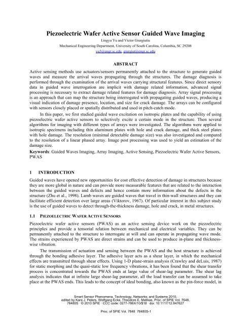
<strong>Piezoelectric</strong> Wafer Active Sensor Guided Wave ImagingLingyu Yu and Victor Giurgiutiu<strong>Mechanical</strong> Engineering Department, University of South Carolina, Columbia, SC 29208yu3@engr.sc.edu, giurgiut@engr.sc.eduABSTRACTActive sensing methods use actuators/<strong>sensor</strong>s permanently attached to the structure to generate <strong>guided</strong><strong>wave</strong>s and measure the arrival <strong>wave</strong>s propagating through the structures. The damage diagnosis isperformed through the examination of the arrival <strong>wave</strong>s carrying structural features. Since direct <strong>sensor</strong>ydata in <strong>guided</strong> <strong>wave</strong> interrogation are implicit with damage related information, advanced signalprocessing is necessary to extract damage related features for damage diagnosis. Array signal processingis an approach that can map the structure being interrogated with propagating <strong>guided</strong> <strong>wave</strong>s, producing avisual indication of damage presence, location, and size for crack damage. The arrays can be configuredwith <strong>sensor</strong>s closely placed or spatially distributed and used in pitch-catch mode.In this paper, we first studied <strong>guided</strong> <strong>wave</strong> excitation on isotropic plates and the capability of usingpiezoelectric <strong>wafer</strong> <strong>active</strong> <strong>sensor</strong>s to selectively excite a certain mode in the structure. Then severalalgorithms for <strong>imaging</strong> with different types of arrays were investigated. The algorithms were applied toisotropic specimens including thin aluminum plates with hole and crack damage, and thick steel plateswith hole damage. The resolution (minimal detectable damage size) was also investigated and comparedto the resolution of a linear phased array. Image post processing was used to yield an estimation of thedamage size.Keywords: Guided Waves Imaging, Array Imaging, Active Sensing, <strong>Piezoelectric</strong> Wafer Active Sensors,PWAS1 INTRODUCTIONGuided <strong>wave</strong>s have opened new opportunities for cost effective detection of damage in structures becausethey are more global in nature and can provide more measurable features that are related to the interactionbetween the <strong>guided</strong> <strong>wave</strong>s and defects and hence contain more information about the defects in thestructure (Zhu et al., 1998). Lamb <strong>wave</strong>s are <strong>guided</strong> <strong>wave</strong>s that travel in thin-wall structures and they canfacilitate efficient detection over large areas (Viktorov, 1967). Of particular interest in this subject studyis the use of <strong>guided</strong> <strong>wave</strong>s to detect through-the-thickness damage, hole and crack, in metal structures.1.1 PIEZOELECTRIC WAFER ACTIVE SENSORS<strong>Piezoelectric</strong> <strong>wafer</strong> <strong>active</strong> <strong>sensor</strong>s (PWAS) as an <strong>active</strong> sensing device work on the piezoelectricprinciples and provide a tensorial relation between mechanical and electrical variables. They can bepermanently attached to the structure to interrogate at will and can operate in propagating <strong>wave</strong> mode.The strains experienced by PWAS are direct strains and can be used to produce in-plane and thicknesswisevibration.The transmission of actuation and sensing between the PWAS and the host structure is achievedthrough the bonding adhesive layer. The adhesive layer acts as a shear layer, in which the mechanicaleffects are transmitted through shear effects. Using 1-D plane-strain analysis (Crawley and deLuis, 1987)for static morphing and the quasi-static low frequency vibrations, it has been found that the shear transferprocess is concentrated towards the PWAS ends at large value of shear-lag parameter. The shear laganalysis indicates that at infinite large shear-lag parameter, all the load transfer can be assumed to takeplace at the PWAS ends. This leads to the concept of ideal bonding, also known as the pin-force model, inSmart Sensor Phenomena, Technology, Networks, and Systems 2010,edited by Kara J. Peters, Wolfgang Ecke, Theodore E. Matikas, Proc. of SPIE Vol. 7648,76480S · © 2010 SPIE · CCC code: 0277-786X/10/$18 · doi: 10.1117/12.847627Proc. of SPIE Vol. 7648 76480S-1
which all the load transfer takes place over an infinitesimal region at the PWAS ends, and the inducedstrainaction is assumed to consist of a pair of concentrated forces applied at the ends.For embedded NDE applications, PWAS can be used as embedded ultrasonic transducers acting aseither actuators to excite <strong>guided</strong> <strong>wave</strong>s or as <strong>sensor</strong>s to receive the structural response in the pitch-catchmode (as illustrated in Figure 1). PWAS couple their in-plane motion with the particle motion of Lamb<strong>wave</strong>s on the material surface while the in-plane motion is excited by the applied oscillatory voltagethrough the d 31 coefficient.In plane pitch-catchV in (t)V out (t)Figure 1PWAS embedded NDE in pitch-catch mode as actuator and <strong>sensor</strong>1.2 TUNED PWAS LAMB WAVESFor Lamb <strong>wave</strong>s, there are at least two <strong>wave</strong> modes, A0 and S0, existing simultaneously where theproduct of the <strong>wave</strong> frequency and structure thickness falls in the range of 0~1 MHz-mm. The tuning ofLamb <strong>wave</strong> attempts to modify the excitation parameters such as to excite certain mode for detectingcertain damage. With wedge-coupled conventional ultrasonic transducers, <strong>guided</strong> <strong>wave</strong> tuning isperformed by varying the frequency and the wedge angle until a maximum response is recorded. Thechange in frequency modifies the <strong>wave</strong> speed of the dispersive <strong>guided</strong> <strong>wave</strong>, while the change of wedgeangle modifies the <strong>wave</strong> conversion relationship in Snell’s law. Certain combinations of wedge-anglesand excitation frequencies were able to generate increasing response in certain <strong>guided</strong>-<strong>wave</strong> modes. Animportant characteristic of PWAS, which distinguishes them from the conventional ultrasonic transducers,is their capability of exciting multiple <strong>guided</strong> <strong>wave</strong> modes at a single frequency. A comprehensive studyof these prediction formulae in comparison with experimental results has been given by Giurgiutiu (2008).By carefully selecting PWAS length at an odd multiple or at an even multiple of the half <strong>wave</strong>length, acomplex pattern of strain maxima and minima emerges. Since several Lamb modes, each with its owndifferent <strong>wave</strong>length, coexist at the same time, a selected Lamb mode can be tuned by choosing theappropriate frequency and PWAS dimensions.A tuning example is given here. On a 1-mm thick aluminum plate installed with 7-mm round PWAS,within an operation frequency range of 0-500 kHz, two Lamb <strong>wave</strong> modes (A0 and S0) existsimultaneously (Figure 2). However, as shown in the strain plot (Figure 2a), there are frequency valueswhere one of the two modes is nearly suppressed. At 300 kHz, A0 mode vibration is very small leavingthe S0 mode dominates. Group velocity vs. frequency plots of S0 and A0 modes are shown in figure 5b.We can see that within the 0~500 kHz range, the S0 mode velocity is almost constant, i.e., the S0 mode ismuch less dispersive compared to the A0 mode.Proc. of SPIE Vol. 7648 76480S-2
A0S0A0S0(a)Figure 2(b)Frequency tuning for PWAS sparse array <strong>imaging</strong>: (a) pitch-catch voltage measurement; (b) dispersioncurves2 PWAS LAMB WAVE PHASED ARRAY IMAGINGThe PWAS phased array application allows large structural areas to be monitored from a single location.The phased array application utilizes the beam steering concepts differentially firing various elements ofthe phased array such that constructive/destructive interference of all the transducers forms a <strong>wave</strong> beamin a certain direction (Giurgiutiu, 2008). Our previous work also showed that the minimum detectable sizeon 1-mm aluminum plate using a linear 8-PWAS (7-mm in diameter) phased array is 1.57 mm.An example of using a linear 8-PWAS phased array to detect and locate a 20-mm simulated crackon a 1-mm aluminum plate is given in Figure 3a. The phased array was installed in the middle of the plateand used to scan the upper side from 0º to 180º. In the array, <strong>sensor</strong>s were put side by side with 1-mm gap.To interrogate, each PWAS takes turn to serve as the actuator sending out a 3-count toneburst signalwhile others are used as <strong>sensor</strong>s to receive the structural responses in a round-robin pattern. After the dataare collected, they are post-processed by the embedded ultrasonic structural radar (EUSR) algorithm(Giurgiutiu et al., 2006) to generate the virtual beam and the scanning 2-D image (Yu and Giurgiutiu,2007). The result is shown in Figure 3b. A highlighted shade about 305 mm in front of the array at 90ºclearly indicates the presence of the broadside crack in the plate. However, to measure the size of thecrack, additional image processing need to be developed.ScanningbeamBroadsidecrack broadsside305 mm610 mm(24.00 in)0ºFigure 3PWAS array570 mm(Meter)(22 45 i)PWAS phased array <strong>imaging</strong> on 1-mm aluminum plate with a 20-mm broadside crack. (a) Specimenlayout; (b) scanning image of the upper side of the plateProc. of SPIE Vol. 7648 76480S-3
3 PWAS LAMB WAVE SPARSE ARRAY IMAGING3.1 SPARSE ARRAY DAMAGE DETECTIONUnlike phased arrays where <strong>sensor</strong>s are physically close to each other, sparse arrays consist of a networkof PWAS transducers spatially distributed and are used to scan the area in and outside the array. In thenetwork, one PWAS sends out interrogating <strong>guided</strong> <strong>wave</strong>. When the <strong>wave</strong> encounters damage, the <strong>wave</strong>gets scattered (Figure 4a). By the comparison of the pristine and damaged <strong>wave</strong> signals, a scatter signalcan be extracted. One advantage of using scatter signals is to minimize the influence caused byboundaries or other structural feature which would otherwise complicate the Lamb <strong>wave</strong> analysis.Analysis of the scattered signals between each pitch-catch pairs permits the correlation of the <strong>wave</strong>propagation in the structure with the damage progression.The image construction of the sparse array is based on a synthetic time reversal concept (Wang etal., 2004) by shifting back the scatter signals at time quantities defined by the transmitter-receiverlocations used in the pitch-catch mode. Figure 4b and Figure 4c illustrates the <strong>imaging</strong> approach.Assuming a single damage scatter is located at point Z(x, y) in the structure, the scatter signal fromtransmitter T i to receiver R j contains a single <strong>wave</strong> packet caused by the damage (Figure 4c). The totaltime of traveling τ Z is determined by the locations of the transmitter T i at (x i , y i ), the receiver R j at (x j , y j ),and Z(x, y), as2 2( xi − x) + ( yi − y) + ( x− xj) + ( y−yj)g2 2τZ= (1)cwhere c g is the group velocity of the traveling Lamb <strong>wave</strong>, assuming constant. Using the time-reversalconcept in Wang et al., 2004, when a <strong>wave</strong> packet is shifted back by the quantity defined by thetransducers and the exact position of the damage, i.e., τ Z , ideally the peak will be shifted right back to thetime origin. If the <strong>wave</strong> packet is shifted by a quantity defined with otherwise cases (such as τ i and τ O ),the peak will not be shifted right at the time origin (Figure 4c).For an unknown damage, for certain scatter signal with τ Z , the possible locations of the damage is anorbit of ellipse with the transmitter and receiver as the foci (Figure 4b). To locate the damage, ellipsesfrom other scatters (or transmitter-receiver pairs in the network) are needed. For a given network of Mtransducers, a total of M 2 scatter signals will be used if reciprocity is not considered. In our study, twoalgorithms, one based on summation process and the other based on the correlation process, have beenemployed for the <strong>imaging</strong>. Using the summation processing (Michaels and Michaels 2007), the pixelvalue at an arbitrary location Z(x, y) in the scanned plane is defined asMMP ( t ) = ∑∑ s ( τ ), i≠j(2)Z 0ij Zi= 1 j=1where s ij is the scatter signal obtained from the j th receiver when the i th transmitter sends. Using themultiplication processing (Ihn and Chang 2008), the pixel value is defined asMMP ( t ) = ∏∏ s ( τ ), i≠j(3)Z 0ij Zi= 1 j=1Proc. of SPIE Vol. 7648 76480S-4
RT iZ(x, y)ZiZot 0τ ZPeakTR jτ iDamageorbitτ O(a)(b)(c)Figure 4PWAS sparse array <strong>imaging</strong> principle: (a) <strong>wave</strong> scattering; (b) damage orbit; (c) signal shiftingA simple sparse array configuration consisting of four <strong>sensor</strong>s is shown in Figure 5a. It can be usedto detect a damage within or outside the array network. Figure 5b illustrates the triangulation principleused to locate the damage. Details of principles and applications of triangulation in damage detection canbe found in many references and will not be described in this paper. In triangulation approach, aminimum of three <strong>sensor</strong>s are required in order to locate the damage. However, when the damageaccidentally falls into the line between two <strong>sensor</strong>s, triangulation will be invalid and fail in locating thedamage. Therefore, in sparse array application, usually a minimum of four <strong>sensor</strong>s is required to correctlyidentify and localize the presence of damage.Sensor #1Sensor #4DamageorbitDamageFigure 5Sensor #2(a)Sensor #3Sparse array <strong>imaging</strong>: (a) a simple sparse array configuration; (b) triangulation principle(b)SensorsIdentifieddamage3.2 SPARSE ARRAY HOLE DETECTIONThe sparse array <strong>imaging</strong> test was conducted on a 1-mm aluminum plate to detect the development of athrough-hole located at (328 mm, 326 mm). Four PWAS were installed on the plate at random locations(Figure 6a). Scanning frequency was selected at 300 kHz to excite S0 Lamb <strong>wave</strong> mode with a travelingspeed at 5500 m/s. Baseline signals were recorded when the hole had a diameter of 2 mm; then the holewas enlarged to 6 mm and measurements were taken (Figure 6b). Imaging results using the twoaforementioned algorithms are presented in Figure 7. The initial investigation for minimum detectablesize on 1-mm aluminum plate using a 4-PWAS sparse array is initially concluded at 4 mm.Proc. of SPIE Vol. 7648 76480S-5
Baseline50 100 150 200#4t (us)#1Measurement#2Hole50 100 150 200Oyx#3t (us)Scatter signal(a)(b)50 100 150 200t (us) First arrivalFigure 6Sparse array <strong>imaging</strong> of a 1-mm aluminum plate with a hole at (328, 326 mm). (a) Specimen layout; (b)signals from a pitch-catch pair (T i =1, R j =3) signals: baseline with the presence of a 2 mm hole (top),measurement after the hole was enlarged to 6 mm (middle), scatter signal obtained from the subtractionbetween baseline and measurement (bottom).(a)Figure 7(b)Sparse array <strong>imaging</strong> of a 1-mm aluminum plate. (a) Summation algorithm; (b) correlation algorithm.3.3 SPARSE ARRAY CRACK DETECTIONThe test specimen is shown in Figure 8. A total of 7 PWAS were installed randomly with locationsindicated in the plot on the right. After the baseline (pristine) data was recorded, a crack centered at (315,249) were introduced, oriented as indicated (along the line of PWAS #2 and #3, perpendicular to PWAS#0 and #5). The crack was increased in length from 10 mm to 18 mm, 23 mm.Proc. of SPIE Vol. 7648 76480S-6
Figure 8Active crack <strong>imaging</strong> specimen layout.3.3.1 Inside Crack DetectionUsing PWAS 0, 2, 3, 6 given in Figure 8 to form a sparse array, we are going to detect the presence ofcrack (at 10 mm) and its growth to 18 mm and 23 mm, as well as giving a crack size estimation with theyielded image results. The Lamb <strong>wave</strong> mode used here is S0 mode at 310 kHz with a <strong>wave</strong>length around17 mm. The image result of crack of 10 mm is given in Figure 9a. Since the <strong>wave</strong> used for interrogationhas a <strong>wave</strong>length smaller than the damage size, the damage shows up as an intensified spot in theresulting image, clearly and correctly representing the presence and location of the crack. When crackincreases to a size comparable to or larger than the interrogation <strong>wave</strong>length, the two tips of the crackforms two strong scatters of the Lamb <strong>wave</strong> and generated two strong intensified spots on the images,representing the crack’s tips, as shown in Figure 9b and Figure 9c. With the indication of crack tips, wecan easily estimate the size of the crack. For example, for the 23 mm crack, the zoomed in damage imageyielded out the locations of the two crack tips at (309, 255) and (328, 243), giving an estimation of cracksize at 22.47 mm with an error of 2.3%. With the sparse array <strong>imaging</strong>, crack tips can be mapped; andtherefore crack size can be measured immediately.(a)Figure 9(b)4-PWAS sparse array <strong>imaging</strong> for crack detection. (a) Image of 10-mm crack; (b) image of 17.5 mm crackProc. of SPIE Vol. 7648 76480S-7
(309,255)(328,243)Figure 104-PWAS sparse array <strong>imaging</strong> for in-network crack detection. (a) Image of 23-mm crack; (b) zoomed inlocal area for crack size estimation.3.3.2 Outside Crack DetectionWhen PWAS 2, 4, 5, 6 are used to form the sparse array, the crack lies outside the network. Imagingresults are given in Figure 11. Although the detection of 10-mm crack failed, we have obtained clear andcorrect images for 18-mm and 23-mm crack when they are outside the sparse array network.(a)(b)Figure 11(c)4-PWAS sparse array <strong>imaging</strong> for out-network crack detection. (a) Image of 10-mm crack (failed); (b)image of 18-mm crack; (c) image of 23-mm crackProc. of SPIE Vol. 7648 76480S-8
4 ARRAY IMAGING ON THICK STEEL PLATERecently, PWAS has been tried on thick steel bridge structures to detect crack growth in both passive and<strong>active</strong> modes (Yu et al., 2009). In <strong>active</strong> mode, PWAS network was intended to scan the entire specimenand present the detection result as a 2-D image. To initiate such a study, we tested a five PWAS sparsearray network on a 24x24x½ (unit: inch) square steel plate (Figure 12a).To obtain appropriate <strong>guided</strong> <strong>wave</strong>s for damage analysis, frequency tuning was conducted first.Figure 13 shows the strain curves and dispersion curves obtained from <strong>wave</strong>scope software within 0-425kHz range (Giurgiutiu 2008). It can be seen the <strong>wave</strong> excitation is very complicated on the thick plate. Asingle mode nondispersive signal is very difficult to obtain in this situation and the sparse array <strong>imaging</strong>failed. A statistics based <strong>imaging</strong> algorithm called RAPID (reconstruction algorithm for probabilisticinspection of defects) was then used (Zhao et al., 2007) to identify the possibility of the damage present ata certain point in the structure without requiring prior knowledge of the <strong>wave</strong> propagation such as <strong>wave</strong>modes and velocity. The <strong>imaging</strong> result is shown in Figure 12b. The highlighted area shows the highestpossibility of damage presence which is a zone centered around (318, 356). Though with deviation, suchan image gave a correct indication of the damage presence and a close estimation of location.10Actual holelocation27.9 mm hole(324, 315)4(a)3(b)Figure 12Thick steel hole detection. (a) ½” steel plate with 5 PWAS installed, a 7.9 mm hole was introduced later; (b)image result of the hole detection at 138 kHz(a)Figure 13Lamb <strong>wave</strong> tuning curves on ½” steel specimen. (a) group velocity; (b) strain curve.(b)Proc. of SPIE Vol. 7648 76480S-9
5 CONCLUSIONSIn this paper, several ultrasonic <strong>guided</strong> <strong>wave</strong> <strong>imaging</strong> approaches using piezoelectric <strong>wafer</strong> <strong>active</strong> <strong>sensor</strong>arrays were presented. The <strong>imaging</strong> approaches were applied to thin aluminum plate and thick steel platespecimens to detect through-the-thickness damage and have obtained good results.The linear PWAS phased array algorithm uses a group of <strong>sensor</strong>s physically close to each other andexcited at certain time interval. The beamforming and damage detection do not require the usage ofbaseline data and can provide a resolution as small as 1.7 mm on 1-mm aluminum plate when eightPWAS were used. Limitations include that the linear array can only scan half part of the specimen andneeds additional <strong>imaging</strong> processing to estimate the crack size.The sparse array uses the scattering signals, requiring the access to baseline data. However, it hasthe advantages of using a minimum of four <strong>sensor</strong>s and being able to image the entire specimen.Currently, the detection resolution is 4 mm on 1-mm aluminum plate, but this can be improved with useof more <strong>sensor</strong>s. In crack detection, sparse array has the feature that it images the tips of a crack; thereforeit provides a good means of crack size estimation.On thick plate, due to the complexity of <strong>guided</strong> <strong>wave</strong> excitation, statistics based RAPID algorithmwas used which does not require the prior knowledge of <strong>wave</strong> propagation such as modes and propagationspeeds. This approach can provide a simple indication of the presence of the damage and a roughestimation of the damage location. To provide high confidence of damage detection, further study will beconducted.6 ACKNOWLEDGMENTSThis work was performed under the support of the US Department of Commerce, National Institute ofStandards and Technology, Technology Innovation Program, Cooperative Agreement Number70NANB9H9007; and Air Force Office of Scientific Research Grant No. FA9550-09-1-0543.REFERENCESCrawley, E. F.; De Luis, J. (1987) “Use of <strong>Piezoelectric</strong> Actuators as Elements of Intelligent Structures”, AIAAJournal, Vol. 25, No. 10, pp. 1373-1385, 1987Giurgiutiu, V. (2008) Structural Health Monitoring with <strong>Piezoelectric</strong> Wafer Active Sensors, Academic Press (anImprint of Elsevier), Burlington, MA, 2008Giurgiutiu, V., Bao, J., Zagrai, A.N. (2006) “Structural Health Monitoring System Utilizing Guided Lamb WavesEmbedded Ultrasonic Structural Radar”, Patent No. US 6,996,480 B2, Date of Patent Feb. 7, 2006Ihn, J.B.; Chang, F.K. (2008) “Pitch-Catch Active Sensing Methods in Structural Health Monitoring for AircraftStructures”, Journal of Structural Health Monitoring, Vol. 7, No. 1, pp. 5-15Michaels, J.E.; Michaels, T.E. (2007) “Guided Wave Signal Processing and Image Fusion for In Situ DamageLocalization in Plates”, Wave Motion, Vol. 44, pp. 482-492Viktorov, I.A. (1967) Rayleigh and Lamb Waves – Physical Theory and Applications, New York, Plenum PressWang, C.H.; Rose, J.T.; Chang, F.K. (2004) “A Synthetic Time-Reversal Imaging Method for Structural HealthMonitoring”, Smart Materials and Structures, Vol. 13, pp. 415-423Yu, L.; Giurgiutiu, V. (2007) “In-situ Optimized PWAS Phased Arrays for Lamb Wave Structural HealthMonitoring”, Journal of Mechanics of Materials and Structures, Vol. 2, No. 3, pp. 459-488Yu, L.; Giurgiutiu, V.; Ziehl, P.; Ozevin, D. (2009) “<strong>Piezoelectric</strong> Based Sensing in Wireless Steel Bridge HealthMonitoring”, Proceedings of SPIE, Vol. 7249, paper # 7249-50Zhao, X.; Gao, H.; Zhang, G.; Ayhan, B.; Yan, F.; Kwan, C.; Rose, J.L. (2007) “Active Health Monitoring of anAircraft Wing with Embedded <strong>Piezoelectric</strong> Sensor/Actuator Network: I. Defect Detection, Localizationand Growth Monitoring”, Smart Materials and Structures, Vol. 16, pp. 1208-1217Proc. of SPIE Vol. 7648 76480S-10
Zhu, W.; Rose, J.L.; Barshinger, J.N.; Agarwala, V.S. (1998) “Ultrasonic Guided Wave NDT for Hidden CorrosionDetection”, Research in Nondestructive Evaluation, Vol. 10, pp. 205-225Proc. of SPIE Vol. 7648 76480S-11