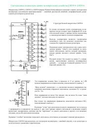
LA4600 - Tehnari.ru
LA4600 - Tehnari.ru
LA4600 - Tehnari.ru
- No tags were found...

You also want an ePaper? Increase the reach of your titles
YUMPU automatically turns print PDFs into web optimized ePapers that Google loves.
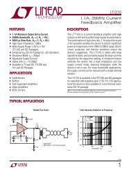
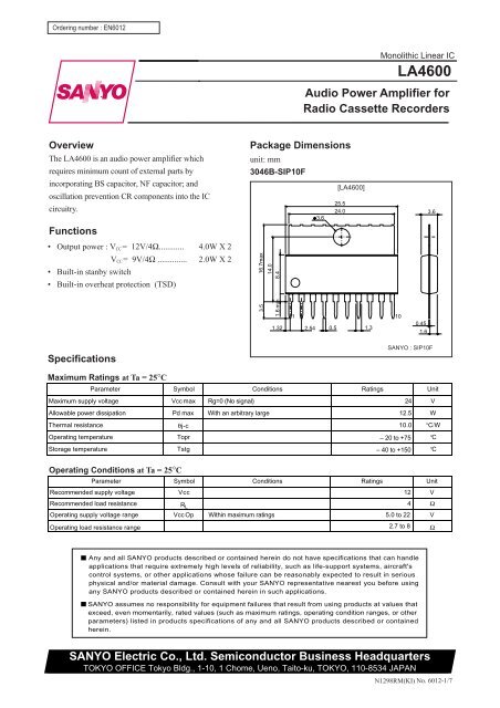
Ordering number : EN6012<strong>LA4600</strong>Monolithic Linear IC<strong>LA4600</strong>. Audio Power Amplifier forRadio Cassette RecordersOverviewThe <strong>LA4600</strong> is an audio power amplifier whichrequires minimum count of external parts byincorporating BS capacitor, NF capacitor; andoscillation prevention CR components into the ICcircuitry.Functions• Output power : V CC = 12V/4Ω............ 4.0W X 2V CC = 9V/4Ω .............. 2.0W X 2• Built-in stanby switch• Built-in overheat protection (TSD)Package Dimensionsunit: mm3046B-SIP10F16.7max14.08.43.6[<strong>LA4600</strong>]25.524.03.63.51.6 min1.3212.540.51.3100.451.6SpecificationsSANYO : SIP10FMaximum Ratings at Ta = 25°CParameter Symbol Conditions Ratings UnitMaximum supply voltage Vcc max Rg=0 (No signal) 24 VAllowable power dissipation Pd max With an arbitrary large 12.5 WThermal resistance θj-c 10.0 °C/WOperating temperature Topr – 20 to +75 °CStorage temperature Tstg – 40 to +150 °COperating Conditions at Ta = 25°CParameter Symbol Conditions Ratings UnitRecommended supply voltage Vcc 12 VRecommended load resistance R L4 ΩOperating supply voltage range Vcc Op Within maximum ratings 5.0 to 22 VOperating load resistance range2.7 to 8 ΩAny and all SANYO products described or contained herein do not have specifications that can handleapplications that require extremely high levels of reliability, such as life-support systems, aircraft'scontrol systems, or other applications whose failure can be reasonably expected to result in seriousphysical and/or material damage. Consult with your SANYO representative nearest you before usingany SANYO products described or contained herein in such applications.SANYO assumes no responsibility for equipment failures that result from using products at values thatexceed, even momentarily, rated values (such as maximum ratings, operating condition ranges, or otherparameters) listed in products specifications of any and all SANYO products described or containedherein.SANYO Electric Co., Ltd. Semiconductor Business HeadquartersTOKYO OFFICE Tokyo Bldg., 1-10, 1 Chome, Ueno, Taito-ku, TOKYO, 110-8534 JAPANN1298RM(KI) No. 6012-1/7
<strong>LA4600</strong>Electrical Characteristics at Ta = 25°C, VCC=12V, RL=4Ω , f=1 kHzParameter Symbol ConditionsRatingsUnitmin typ maxStandby current Ist Standby pin —> GND 1.0 10 µAQuiescent current Icco Rg=0 18 32 64 mAVoltage gain VG Vo=0dBm 43.0 45.0 47.0 dBTotal harmonic distortion THD Po=1w 0.2 0.8 %Output noise voltage Vno Rg=0, DIN AUDIO 0.15 0.5 mVOutput voltage Po1 THD=10% 3.0 4.0 WPo2 Vcc=9V, THD=10% 1.5 2.0 WChannel separation Chsep Vo=0dBm, Rg=0, DIN AUDIO 50 60 dBRipple rejection ratio SVRR Vr=0dBm, Rg=0, fr=100 Hz DIN AUDIO 45 55 dBStanby ON voltage Vst 1.5 5.0 VInput resistance Ri 20 30 40 KΩBlock DiagramStandby7Vcc4Standby switchingCH1 input10CH1 inputamplifierPredriveamplifierOutputamplifier1CH1 outputR f1R Nf1Small signalGND9R Nf2REFamplifierR f2TSD protector2Large signalGNDCH2 input8CH2 inputamplifierPredriveamplifierOutputamplifier3CH2 outputPop noise prevention blockRipple filter6 5P.PFilterNo. 6012-2/7
++<strong>LA4600</strong>Sample Application+5V+1000µF7STANDBY4VCC0.22µF10 ch1Inputch1Output1+1000µF4Ω9PRE GND<strong>LA4600</strong>POWER GND20.22µF8ch2Inputch2Output3+1000µF 4ΩP.P6+Filter5+4.7µF 100µFAllowable power dissipation, Pd max – W14121086542Pd max – TaWith an arbitrary large heatsink (θjc=10˚C/W)12.550X50X1.5mm 3 1.94No heatsink1.160–20 0 20 40 60 80 100Ambient temperature, Ta – ˚C7.53.0No. 6012-3/7
<strong>LA4600</strong>Pin Descriptions1. Standby switching function (7)VCCPower is switched ON and OFF by controlling the High and Low states at pin7, respectively (standby). To switch power ON, apply 1.5V or more, or 800µA to pin 7.To bias circuitApplied voltage Applied voltage – V BE (approx. 0.7V)Current supplied to pin 7 = . .+2 kΩ 2 kΩ• When directly connecting a microcontroller with this pin, add a resistor in seriesto optimize the current for the microcontroller.72kΩ2kΩ2. Input pins (8,10)Voltage at the input pins is approx. 2 V BE (1.4V).Input impedance is approx. 30 kΩ.• The recommended value for the input capacitor is 0.22 µF, but this can be varied in order to adjust the starting time(ts). (The starting time is the time required from applying voltage to the standby pin until sound output is obtained. )Input capacitator 1.0 µF 2.0 µF 3.3 µF 4.7 µF 10 µFStarting time (t s ) 0.2s 0.3s 0.5s 0.65s 1.5s3. Filter (decoupling) pin (5)Pin voltage is approx. 1/2 V CC .The recommended value for the filter capacitor is 100 µF.When capacitance is lower, pop noise when setting the standby pin to Low (power OFF) will increase.Filter capacitor= 100 µ Filter capacitor= 47 µFAC voltage (100 mV)AC voltage (200mV)Output DC voltageOutput DC voltageNo. 6012-4/7
<strong>LA4600</strong>4. P.P (pop noise) pin (6)VCCVoltage at pin 6.= .V CC – V CE (approx. 0.3V) – 5.6V2+ 5.6V• The recommended value for the P.P capacitor is 4.7 µF.When capacitance is lower than 2.2 µF, pop noise when setting the standbypin to Low (power OFF) will increase.When capacitance is higher than 10 µF, the sound will not be cut off whensetting the standby pin to Low (power OFF).65kΩ5kΩZener voltage= 5.6VTo input amplifier/bias circuitry5. MutingThe output signal can be controlled byconnecting pin 5 (Filter) to ground via aresistance of 300 to 500 Ω. If resistanceis higher than 750 Ω, the suppressionratio will decrease.Output AC voltageOutput DC voltageMute ONMute OFFNo. 6012-5/7
<strong>LA4600</strong>Output power, PO – W10987654321RL=3ΩVCC – PORL=4ΩRL=8ΩTHD=10%f=1kHzQuiescent current, ICCO – mA8070605040302010VCC – ICCORg=0Total harmonic distortion, THD – %Channel separation, Chsep – dBResponse – dB04 8 12 162024Supply Voltage, V CC – V1075321.075320.175320.010.0110 2 3 5 7 100 2 3 5 7 1k 2 3 5 710k 2 3 5 7 100k 0.1 2 3 5 7 1.0 2 3 5 7 10Frequency, f – HzOutput power, PO – W8070605040VCC=12VRL=4Ω30 VO=0dBmRg=0DIN AUDIO202 3 5 7 100 2 3 5 7 1k 2 3 5 7 10k 2 3Frequency, f – Hz10–1–2–3–4–5–6–7Cout=2200µFCout=1000µFch2-ch12ch1chch1-ch2THD – fChsep – ff – ResponseV CC =12VR L =4ΩP O =1WRg=600ΩV CC =12VR L =4ΩV O =0dBm04 8 12 16 20 24 28Supply Voltage, V CC –V–8010 2 3 5 7 100 2 3 5 7 1k 2 3 5 7 10k 2 3 5 7 100k 5 7 1k 2 3 5 7 10k 2 3 5 7Frequency, f – HzSignal source impedance, Rg – ΩTotal harmonic distortion, THD – %Ripple rejection, SVRR – dBOutput noise voltage, VNO – mV10075321075321.075320.17532807060504030202 3 5 7 100 2 3 5 7 1k 2 3Frequency, f – Hz1.00.90.80.70.60.50.40.30.20.1V CC =12VR L =4ΩP O =1WRg=600ΩTHD – POSVRR – fch1ch22ch1chVNO – RgVCC=12VRL=4ΩVr=0dBmRg=0DIN AUDIOV CC =12VR L =4ΩDIN AUDIONo. 6012-6/7