EM4006
EM4006
EM4006
- No tags were found...

You also want an ePaper? Increase the reach of your titles
YUMPU automatically turns print PDFs into web optimized ePapers that Google loves.
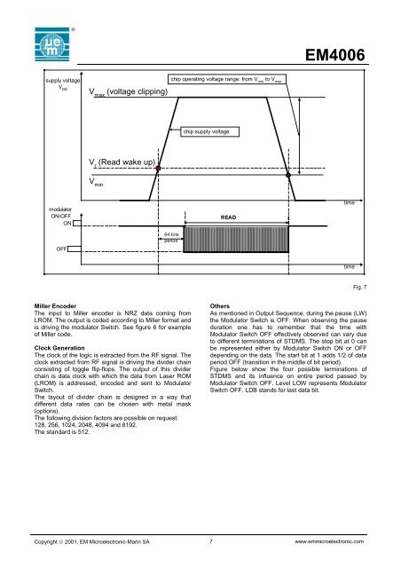
<strong>EM4006</strong>supply voltageV DDV max(voltage clipping)chip operating voltage range: from V minto V maxchip supply voltageV r(Read wake up)V minmodulatorON/OFFONREADtimeOFF64 bitsperiodtimeFig. 7Miller EncoderThe input to Miller encoder is NRZ data coming fromLROM. The output is coded according to Miller format andis driving the modulator Switch. See figure 6 for exampleof Miller code.Clock GenerationThe clock of the logic is extracted from the RF signal. Theclock extracted from RF signal is driving the divider chainconsisting of toggle flip-flops. The output of this dividerchain is data clock with which the data from Laser ROM(LROM) is addressed, encoded and sent to ModulatorSwitch.The layout of divider chain is designed in a way thatdifferent data rates can be chosen with metal mask(options).The following division factors are possible on request:128, 256, 1024, 2048, 4094 and 8192.The standard is 512.OthersAs mentioned in Output Sequence, during the pause (LW)the Modulator Switch is OFF. When observing the pauseduration one has to remember that the time withModulator Switch OFF effectively observed can vary dueto different terminations of STDMS. The stop bit at 0 canbe represented either by Modulator Switch ON or OFFdepending on the data. The start bit at 1 adds 1/2 of dataperiod OFF (transition in the middle of bit period).Figure below show the four possible terminations ofSTDMS and its influence on entire period passed byModulator Switch OFF. Level LOW represents ModulatorSwitch OFF. LDB stands for last data bit.Copyright © 2001, EM Microelectronic-Marin SA 7 www.emmicroelectronic.com