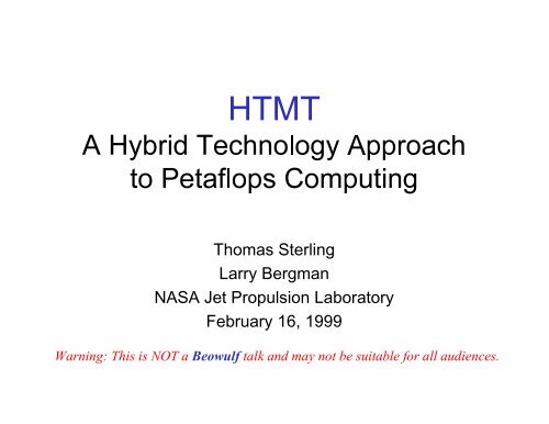
HTMT: A Hybrid Technology Approach to Petaflops Computing
HTMT: A Hybrid Technology Approach to Petaflops Computing
HTMT: A Hybrid Technology Approach to Petaflops Computing

Create successful ePaper yourself
Turn your PDF publications into a flip-book with our unique Google optimized e-Paper software.
Thomas SterlingLarry BergmanNASA Jet Propulsion Labora<strong>to</strong>ryFebruary 16, 1999Warning: This is NOT a Beowulf talk and may not be suitable for all audiences.
February 16, 1999 <strong>Petaflops</strong> II - <strong>HTMT</strong> Architecture 2
• Scalable architecture with high sustainedperformance in the presence of disparate cycle timesand latencies• Exploit diverse device technologies <strong>to</strong> achievesubstantially superior operating point• Execution model <strong>to</strong> simplify parallel systemprogramming and expand generality and applicabilityFebruary 16, 1999 <strong>Petaflops</strong> II - <strong>HTMT</strong> Architecture 3
3DMemDRAMPIMI/O FARM• Compress/Decompress• Spectral Transforms• Data StructureInitializations•“In the Memory”OperationsOPTICAL SWITCHSRAMPIMRSFQNodes• Compress/Decompress• ECC/Redundancy• Compress/Decompress• Routing• RSFQ Thread Management• Context Percolation• Scatter/Gather Indexing• Pointer chasing• Push/Pull Closures• Synchronization ActivitiesFebruary 16, 1999 <strong>Petaflops</strong> II - <strong>HTMT</strong> Architecture 4
• processor: 150 GHz, 600 Gflops• # processors: 2048• memory: 16 Tbytes PIM-DRAM, 80ns access time• interconnect: Data Vortex, 500 Gbps/channel, > 10Pbps bi-section bw• 3/2 s<strong>to</strong>rage: 1 Pbyte, 10 us access time• shared memory, 4 level hierarchy• latency management: multithreaded with percolationFebruary 16, 1999 <strong>Petaflops</strong> II - <strong>HTMT</strong> Architecture 5
February 16, 1999 <strong>Petaflops</strong> II - <strong>HTMT</strong> Architecture 6
S<strong>to</strong>rage Capacity by Subsystem2007 Design PointSubsystem Unit S<strong>to</strong>rage # of Units Total S<strong>to</strong>rageCRAM 32 KB 16 K 512 MBSRAM 64 MB 16 K 1 TBDRAM 512 MB 32 K 16 TBHRAM 10 GB 128 K 1 PBPrimary Disk 100 GB 100 K 10 PBSecondary Disk 100 GB 100 K 10 PBTape 1 TB 6Kx20 120 PBFebruary 16, 1999 <strong>Petaflops</strong> II - <strong>HTMT</strong> Architecture 7
February 16, 1999 <strong>Petaflops</strong> II - <strong>HTMT</strong> Architecture 8
• High performance– Superconduc<strong>to</strong>r RSFQ logic– Data Vortex optical interconnect network– PIM smart memory• Low power– Superconduc<strong>to</strong>r RSFQ logic– Optical holographic s<strong>to</strong>rage– PIM smart memoryFebruary 16, 1999 <strong>Petaflops</strong> II - <strong>HTMT</strong> Architecture 9
• Low cost– reduce wire count through chip-<strong>to</strong>-chip fiber– reduce processor count through x100 clock speed– reduce memory chips by 3-2 holographic memory layer• Efficiency– processor level multithreading– smart memory managed second stage context pushingmultithreading– fine grain regular & irregular data parallelism exploited in memory– high memory bandwidth and low latency ops through PIM– memory <strong>to</strong> memory interactions without processor intervention– hardware mechanisms for synchronization, scheduling,data/context migration, gather/scatterFebruary 16, 1999 <strong>Petaflops</strong> II - <strong>HTMT</strong> Architecture 10
• Programmability– Global shared name space– hierarchical parallel thread flow control model• no explicit processor naming– au<strong>to</strong>matic latency management• au<strong>to</strong>matic processor load balancing• runtime fine grain multithreading• au<strong>to</strong>matic context pushing for process migration (percolation)– configuration transparent, runtime scalableFebruary 16, 1999 <strong>Petaflops</strong> II - <strong>HTMT</strong> Architecture 11
DARPAJ. MuniozNSAG. CotterDoc BedardW. Carlson (IDA)NASAE. TuW. Johns<strong>to</strong>nSTEERINGCOMMITTEEP. MessinaPIT. SterlingProject MgrL. BergmanSoftwareCoordinationL. CraymerProject AAD. CrawfordProject SecretaryA. SmytheSystem Engineer(S. Monacos)Tech PublishingM. MacDonaldCACRCO-IP. MessinaCALTECHCO-ID. PsaltisNOTRE DAMECO-IP. KoggeSUNYCO-IK. LikharevPRINCETONCO-IK. BergmanC. Reed (IDA)UNIVERSITYOF DELAWARECO-IG. GaoARGONNECO-IR. StevensTERACO-IB. SmithUCSBCI-IM. RodwellM. Melliar-SmithRPICI-IJ. McDonaldUniv RochesterCI-IM. FeldmanJPLCO-IT. CwikJPLCO-ID. CurkendallH. SiegelTRWCI-IA. SilverHYPRESSCI-IE. TrackTICI-IG. ArmstrongFebruary 16, 1999 <strong>Petaflops</strong> II - <strong>HTMT</strong> Architecture 12
• Concepts and Structures– approach strategy– device technologies– subsystem design– efficiency, productivity,generality• System Architecture– size, cost, complexity, power• System Software– resource management– multiprocessor emula<strong>to</strong>r• Applications– multithreaded codes– scaling models• Evaluation– feasibility– cost– performance• Future Directions– Phase 3 pro<strong>to</strong>type– Phase 4 petaflops system– ProposalsFebruary 16, 1999 <strong>Petaflops</strong> II - <strong>HTMT</strong> Architecture 13
(VLSI CircuitClockFrequency)1 THz100 GHz10 GHz3.5 umhigh-Tc (65-77 K)RSFQlow-Tc (4-5 K)0.8 um??0.25 um0.4 um1.5 umpetaflops-scalecomputing (??)single-node super-workstations (?)digital communication switchesdigital signal processorsdigital signal correla<strong>to</strong>rs and modemsanalog-<strong>to</strong>-digital convertersdigital-<strong>to</strong>-analog convertersarbitrary waveform genera<strong>to</strong>rsdigital SQUIDs1 GHzoptical lithgraphy0.25 um0.13 um??e-beam lithgraphyCMOS(SIA Forecast)0.07 um100MHz199820012004 20072010YearFebruary 16, 1999 <strong>Petaflops</strong> II - <strong>HTMT</strong> Architecture 14
February 16, 1999 <strong>Petaflops</strong> II - <strong>HTMT</strong> Architecture 15
• X100 clock speeds achievable• X100 power efficiency advantage• Easier fabrication• Leverage semiconduc<strong>to</strong>r fabrication <strong>to</strong>ols• First technology <strong>to</strong> encounter ultra-high speedoperationFebruary 16, 1999 <strong>Petaflops</strong> II - <strong>HTMT</strong> Architecture 16
• 100 GHz clock, 33 GHz inter-chip• 0.8 micron Niobium on Silicon• 100K gates per chip• 0.05 watts per processor• 100Kwatts per <strong>Petaflops</strong>February 16, 1999 <strong>Petaflops</strong> II - <strong>HTMT</strong> Architecture 17
• SPELL Architecture• Detailed circuit design for critical paths• CRAM Memory design initiated• 1st network design and analysis/simulation• 750 GHz logic demonstrated• Detailed sizing, cost, and power analysis• Estimate for fabrication facilities investment• Barriers and path <strong>to</strong> 0.4-0.25 micron regime• Sizing for Phase 3 50 Gflops processorFebruary 16, 1999 <strong>Petaflops</strong> II - <strong>HTMT</strong> Architecture 18
Data Vortex OpticalInterconnectFebruary 16, 1999 <strong>Petaflops</strong> II - <strong>HTMT</strong> Architecture 19
February 16, 1999 <strong>Petaflops</strong> II - <strong>HTMT</strong> Architecture 20
DATA VORTEX LATENCY DISTRIBUTIONnetwork height = 1024120x103number of messages1008060402022% active input ports100% active input ports00204060number of hops80100February 16, 1999 <strong>Petaflops</strong> II - <strong>HTMT</strong> Architecture 21
SiO2claddingOpticalmodeSingle-mode rib waveguideson silicon-on-insula<strong>to</strong>r wafers ‡<strong>Hybrid</strong> sources and detec<strong>to</strong>rsSiBuriedoxide‡ e.g:Mix of CMOS-like and‘micromachining’-typeprocesses for fabricationSi substrateR A Soref, J Schmidtchen & K Petermann,IEEE J. Quantum Electron. 27 p1971 (1991)A Rickman, G T Reed, B L Weiss & F Navamar,IEEE Pho<strong>to</strong>nics Technol. Lett. 4 p.633 (1992)B Jalali, P D Trinh, S Yegnanarayanan & FCoppingerIEE Proc. Op<strong>to</strong>electron. 143 p.307 (1996)February 16, 1999 <strong>Petaflops</strong> II - <strong>HTMT</strong> Architecture 22
• Bi-section sustained bandwidth: 4000 Tbps• Per port data rate: 640 Gbps• Single wavelength channel rate: 10 Gbps• Level of WDM: 64 colors• Number of input ports: 6250• Angle nodes: 7• Network node height: 4096• Number of nodes per cylinder: 28672• Number of cylinders: 13• Total node number: 372736February 16, 1999 <strong>Petaflops</strong> II - <strong>HTMT</strong> Architecture 23
• Implemented and tested optical device technology• Pro<strong>to</strong>typed electro-optical butterfly switch• Design study of electro-optic integrated switch• Implemented and tested most of end-<strong>to</strong>-end path• Design of <strong>to</strong>pology <strong>to</strong> size• Simulation of network behavior under load• Modified structure for ease of packaging• Size, complexity, power studies• Initial interface designFebruary 16, 1999 <strong>Petaflops</strong> II - <strong>HTMT</strong> Architecture 24
Sense AmpsMemoryStackSense AmpsNode LogicSense AmpsMemoryStackSense AmpsDecodeSense AmpsMemoryStackSense AmpsSense AmpsMemoryStackSense AmpsBasicSiliconMacroSingleChip• Merge logic and memory• Integrate multiple logic/memstacks on single chip• Exposes high intrinsicmemory bandwidth• Reduction of memory accesslatency• Low overhead for memoryoriented operations• Manages data structuremanipulation, contextcoordination and percolationFebruary 16, 1999 <strong>Petaflops</strong> II - <strong>HTMT</strong> Architecture 25
Multithreaded Control of PIM Functions• multiple operation sequences with low context switching overhead• maximize memory utilization and efficiency• maximize processor and I/O utilization• multiple banks of rowbuffers <strong>to</strong> hold data,instructions, and addr• data parallel basicoperations at row buffer• manages sharedresources such as FPBoolean ALURow RegistersGP - ALUContext RegistersMemoryStackRow BuffersDirect PIM <strong>to</strong> PIM Interaction• memory communicates with memorywithin and across chip boundarieswithout external control processorintervention by “parcels”• exposes fine grain parallelism intrinsic <strong>to</strong>vec<strong>to</strong>r and irregular data structures• e.g. pointer chasing, block moves,synchronization, data balancingMemoryBus I/F(PCI)Node LogicFPFPHi SpeedLinks(Firewire)February 16, 1999 <strong>Petaflops</strong> II - <strong>HTMT</strong> Architecture 26
• Establish operational opportunity and requirements• Win $12.2M DARPA contract for DIVA– USC ISI prime– Caltech, Notre Dame, U. of Delaware– Deliver 8 Mbyte part in FY01 at 0.25 micron• Architecture concept design complete– parcel message driven computation– multithreaded resource management• Analysis of size, power, bandwidth• Diva <strong>to</strong> be used directly in Phase 3 testbedFebruary 16, 1999 <strong>Petaflops</strong> II - <strong>HTMT</strong> Architecture 27
Performance Scaling1998 2001 2004Module 1 Gbit 1 GB 10 GBcapacityNumber of10 5 10 5modulesAccess time 1 ms 100 µs 10 µsReadout 1 Gb/s .1 PB/s 1 PB/sbandwidthRecordbandwidth1 Mb/s 1 GB/s .1 PB/sAdvantages• petabyte memory• competitive cost• 10 µsec access time• low power• efficient interface <strong>to</strong> DRAMDisadvantages• recording rate is slower than thereadout rate for LiNbO 3• recording must be done in GB chunks• long term trend favors DRAM unlessnew materials and lasers are usedFebruary 16, 1999 <strong>Petaflops</strong> II - <strong>HTMT</strong> Architecture 28
• Detailed study of two optical s<strong>to</strong>rage technologies– pho<strong>to</strong> refractive– spectral hole burning• Operational pho<strong>to</strong> refractive read/write s<strong>to</strong>rage• Access approaches explored for 10 usec regime– pixel array– wavelength multiplexing• Packaging studies• power, size, cost analysisFebruary 16, 1999 <strong>Petaflops</strong> II - <strong>HTMT</strong> Architecture 29
•Extend latency hiding of multithreading•Hierarchy of logical thread•Delineates threads and thread ensembles•Action sequences, state, and precedence constraints•Fine grain single cycle thread switching•Processor level, hides pipeline and time of flight latency•Coarse grain context "percolation"•Memory level, in memory synchronization•Ready contexts move <strong>to</strong>ward processors, pendingcontexts <strong>to</strong>wards big memoryFebruary 16, 1999 <strong>Petaflops</strong> II - <strong>HTMT</strong> Architecture 30
Percolationof threadsFebruary 16, 1999 <strong>Petaflops</strong> II - <strong>HTMT</strong> Architecture 31
• Multiple stage latency managementmethodology• Augmented multithreaded resourcescheduling• Hierarchy of task contexts• Coarse-grain contexts coordinate inPIM memory• Ready contexts migrate <strong>to</strong> SRAMunder PIM control releasing threadsfor scheduling• Threads pushed in<strong>to</strong> SRAM/CRAMframe buffers• Strands loaded in register banks onspace available basisThreads S<strong>to</strong>red in SRAMContextsS<strong>to</strong>red inDRAMStrandsS<strong>to</strong>red inRegsFebruary 16, 1999 <strong>Petaflops</strong> II - <strong>HTMT</strong> Architecture 32
DMA <strong>to</strong> CRAMCRYOGENIC AREAstartdoneSplit-PhaseSynchronization<strong>to</strong> SRAMC-BufferParcelDispatcher&DispenserA-QueueRe-UseD-QueueParcelAssembly&DisassemblyI-QueueT-QueueParcelInvocation&TerminationSRAM-PIMRun Time SystemDMA <strong>to</strong> DRAM-PIMFebruary 16, 1999 <strong>Petaflops</strong> II - <strong>HTMT</strong> Architecture 33
1.4 m 0.3 m1 m77 o K4 o K50 WSIDE VIEWFiber/WireInterconnects1 m3 mFebruary 16, 1999 <strong>Petaflops</strong> II - <strong>HTMT</strong> Architecture 340.5 m
Top Down View of <strong>HTMT</strong> Machine2007 Design PointFebruary 16, 1999 <strong>Petaflops</strong> II - <strong>HTMT</strong> Architecture 35
NitrogenHeliumSIDE VIEW77o K4 o K50 WFiber/WireInterconnectsFront EndComputerServerHard Disk Tape SiloArrayArray(40 cabinets) (400 Silos)3 m3 mConsoleCable Tray Assembly0.5 m220Volts220VoltsGenera<strong>to</strong>r980 nmPumps(20 cabinets)WDM SourceOpticalAmplifiersGenera<strong>to</strong>rFebruary 16, 1999 <strong>Petaflops</strong> II - <strong>HTMT</strong> Architecture 36
<strong>HTMT</strong> Facility (Top View)15 m27 m27 mCryogenicsRefrigeration RoomFebruary 16, 1999 <strong>Petaflops</strong> II - <strong>HTMT</strong> Architecture 3725 m
1. <strong>HTMT</strong> 1,0002. Server 2503. Pump/MG 3,0004. Laser 980 1,0005. Disk Farm (80) 1,6006. Tape Robot Farm (20) 4,0007. Opera<strong>to</strong>r Room 1,000TOTAL = 11,850 sq ftFebruary 16, 1999 <strong>Petaflops</strong> II - <strong>HTMT</strong> Architecture 38
Power Dissipation by Subsystem<strong>Petaflops</strong> Design PointSubsystem Unit Type Unit Power # of Units Total PowerCryostat/Cooling System 400 kW 1 400 kWSRAM PIM 5 W 16 K 80 kWWDM source/amps Port 15 W 4 K 62 kWData Vortex Subnet 2 kW 128 258 kWDRAM PIM 625 mW 32 K 20 kWHRAM HRAM 100 mW 128 K 13 kWPrimary Disk Disk 15 W 100 K 1500 kWTape Silo 1 kW 20 20 kWServer Machine 100 kW 1 100 kWTOTAL2.4 MWFebruary 16, 1999 <strong>Petaflops</strong> II - <strong>HTMT</strong> Architecture 39
Subsystem Interfaces2007 Design PointSubsystem Interface <strong>to</strong> Wires/Port Speed/Wire (bps) #ports Aggregate BW (Byte/s) Wire count type of IFRSFQ SRAM 16000 20.0E+9 512 20.5E+15 8.2E+6 wireSRAM RSFQ 1000 2.0E+9 8000 2.0E+15 8.0E+6 TBDSRAM Data Vortex 1000 2.0E+9 8000 2.0E+15 8.0E+6 wireData Vortex SRAM 1 640.0E+9 2048 163.8E+12 2.0E+3 fiberData Vortex DRAM 1 640.0E+9 2048 163.8E+12 2.0E+3 fiberDRAM Data Vortex 1000 1.0E+9 33000 4.1E+15 33.0E+6 wireDRAM HRAM 1000 1.0E+9 33000 4.1E+15 33.0E+6 wireDRAM Server 1 800.0E+6 1000 100.0E+9 1.0E+3 wireServer DRAM 1 800.0E+6 1000 100.0E+9 1.0E+3 (fiber channel)Server Disk 1 800.0E+6 1000 100.0E+9 1.0E+3 (fiber channel)Server Tape 1 800.0E+6 200 20.0E+9 200.0E+0 (fiber channel)HRAM DRAM 800 100.0E+6 1.00E+05 1.0E+15 80.0E+6 wire•Same colors indicate a connection between subsystems•Horizontal lines group interfaces within a subsystemFebruary 16, 1999 <strong>Petaflops</strong> II - <strong>HTMT</strong> Architecture 40
• System architecture completed• Physical structure design• Parts count, power, interconnect complexity analysis• Infrastructure requirements and impact• Feasibility assessmentFebruary 16, 1999 <strong>Petaflops</strong> II - <strong>HTMT</strong> Architecture 41
• Executable Specification– subsystem functional/operational description– inter-subsystem interface pro<strong>to</strong>col definition• Distributed Low-cost Cluster of processors• Cluster partitioned and allocated <strong>to</strong> separatesubsystems• Subsystem development groups “own” clusterpartitions, and develop functional specification• Subsystem partitions interact by agreed-uponinterface pro<strong>to</strong>cols• Runtime percolation and thread scheduling systemsoftware put on <strong>to</strong>p of emulation software.February 16, 1999 <strong>Petaflops</strong> II - <strong>HTMT</strong> Architecture 42
February 16, 1999 <strong>Petaflops</strong> II - <strong>HTMT</strong> Architecture 43