WM8962B, Rev 4.1 - Wolfson Microelectronics plc
WM8962B, Rev 4.1 - Wolfson Microelectronics plc
WM8962B, Rev 4.1 - Wolfson Microelectronics plc

You also want an ePaper? Increase the reach of your titles
YUMPU automatically turns print PDFs into web optimized ePapers that Google loves.
Production Data<strong>WM8962B</strong>TABLE OF CONTENTSDESCRIPTION ....................................................................................................... 1FEATURES ............................................................................................................ 1APPLICATIONS .................................................................................................... 1BLOCK DIAGRAM ................................................................................................ 2TABLE OF CONTENTS ......................................................................................... 3PIN CONFIGURATION .......................................................................................... 7ORDERING INFORMATION .................................................................................. 7PIN DESCRIPTION ................................................................................................ 8ABSOLUTE MAXIMUM RATINGS ........................................................................ 9RECOMMENDED OPERATING CONDITIONS ..................................................... 9ELECTRICAL CHARACTERISTICS ................................................................... 10TERMINOLOGY ............................................................................................................. 20THERMAL CHARACTERISTICS......................................................................... 21TYPICAL POWER CONSUMPTION .................................................................... 22SIGNAL TIMING REQUIREMENTS .................................................................... 26MASTER CLOCK ........................................................................................................... 26AUDIO INTERFACE TIMING ......................................................................................... 27DIGITAL MICROPHONE (DMIC) INTERFACE TIMING ............................................................................ 27DIGITAL AUDIO INTERFACE - MASTER MODE ..................................................................................... 28DIGITAL AUDIO INTERFACE - SLAVE MODE ......................................................................................... 29DIGITAL AUDIO INTERFACE - TDM MODE ............................................................................................. 30CONTROL INTERFACE TIMING ................................................................................... 312-WIRE (I2C) CONTROL MODE ............................................................................................................... 313-WIRE (SPI) CONTROL MODE ............................................................................................................... 324-WIRE (SPI) CONTROL MODE ............................................................................................................... 33POWER ON RESET TIMING ......................................................................................... 34DEVICE DESCRIPTION ...................................................................................... 37INTRODUCTION ............................................................................................................ 37INPUT SIGNAL PATH .................................................................................................... 38MICROPHONE INPUT CONNECTION ..................................................................................................... 39LINE INPUT CONNECTION ...................................................................................................................... 39MICROPHONE BIAS CONTROL .............................................................................................................. 40MICBIAS CURRENT DETECT .................................................................................................................. 40MICBIAS CURRENT DETECT FILTERING ............................................................................................... 41MICROPHONE HOOK SWITCH DETECTION .......................................................................................... 43MULTIPLE PUSH BUTTON DETECTION ................................................................................................. 44INPUT PGA ENABLE ................................................................................................................................ 45INPUT PGA CONFIGURATION ................................................................................................................ 46INPUT PGA VOLUME CONTROL ............................................................................................................. 47INPUT MIXER ENABLE ............................................................................................................................. 49INPUT MIXER CONFIGURATION AND VOLUME CONTROL .................................................................. 49AUTOMATIC LEVEL CONTROL (ALC) ......................................................................... 52LIMITER MODE ......................................................................................................................................... 54ALC GAIN CONTROL ................................................................................................................................ 56ALC DYNAMIC CHARACTERISTICS........................................................................................................ 57PEAK LIMITER .......................................................................................................................................... 59ALC NOISE GATE ..................................................................................................................................... 60ALC STATUS READBACK ........................................................................................................................ 64wPD, April 2013, <strong>Rev</strong> <strong>4.1</strong>3
Production Data<strong>WM8962B</strong>DE-EMPHASIS FILTER RESPONSES ........................................................................ 283APPLICATIONS INFORMATION ...................................................................... 284ANALOGUE INPUT PATHS .................................................................................................................... 284MICROPHONE BIAS CIRCUIT ............................................................................................................... 284CHARGE PUMP COMPONENTS ........................................................................................................... 286RECOMMENDED EXTERNAL COMPONENTS DIAGRAM .................................................................... 287PCB LAYOUT CONSIDERATIONS ............................................................................. 289MIC DETECTION SEQUENCE USING MICBIAS CURRENT ..................................... 290PACKAGE DIMENSIONS .................................................................................. 292IMPORTANT NOTICE ....................................................................................... 293ADDRESS .................................................................................................................... 293REVISION HISTORY ......................................................................................... 294wPD, April 2013, <strong>Rev</strong> <strong>4.1</strong>6
Production Data<strong>WM8962B</strong>PIN CONFIGURATION1 2 3 4 5 6 7ASPKOUTLPSPKVDD1MICBIASHPOUTRCPVOUTPCPVOUTNBSPKOUTLNHPOUTFBHPOUTLCPCACPCBCSPKGND2SPKVDD2SPKOUTRNIN1LVMIDCCPVDDCPGNDDDACDATADCDATLRCLKIN1RIN2LAVDDAGNDEBCLKSDACS/GPIO6CLKOUT2/GPIO2IN2RIN4LIN4RFSCLKCIFMODEDGNDCLKOUT3/GPIO3IN3LIN3RXTOGGPIO5DCVDDDBVDDPLLVDDCLKOUT5MCLK/XTIORDERING INFORMATIONORDER CODE TEMPERATURE RANGE PACKAGE MOISTURESENSITIVITY LEVEL<strong>WM8962B</strong>ECSN/R -40C to +85C 49-ball CSP(3.6x3.9mm)(Pb-free, Tape and reel)Note:Reel quantity = 5,000PEAK SOLDERINGTEMPERATUREMSL1 260°CwPD, April 2013, <strong>Rev</strong> <strong>4.1</strong>7
Production Data<strong>WM8962B</strong>ABSOLUTE MAXIMUM RATINGSAbsolute Maximum Ratings are stress ratings only. Permanent damage to the device may be caused by continuously operating at orbeyond these limits. Device functional operating limits and guaranteed performance specifications are given under ElectricalCharacteristics at the test conditions specified.ESD Sensitive Device. This device is manufactured on a CMOS process. It is therefore generically susceptibleto damage from excessive static voltages. Proper ESD precautions must be taken during handling and storageof this device.<strong>Wolfson</strong> tests its package types according to IPC/JEDEC J-STD-020 for Moisture Sensitivity to determine acceptable storageconditions prior to surface mount assembly. These levels are:MSL1 = unlimited floor life at
Production Data<strong>WM8962B</strong>ELECTRICAL CHARACTERISTICSTest ConditionsMICVDD = DCVDD = DBVDD = CPVDD = AVDD = PLLVDD = 1.8V, SPKVDD1 = SPKVDD2 = 5V.T A = +25 o C, 1kHz signal, fs = 48kHz, PGA gain = 0dB, 24-bit audio data unless otherwise stated.PARAMETER SYMBOL TEST CONDITIONS MIN TYP MAX UNITAnalogue Inputs (IN1L, IN1R, IN4L, IN4R) to Input PGAFull-scale Input Signal Level – notethis changes in proportion to AVDDV INFS Single-ended PGA input 500-6.02Input resistance +24dB PGA gain 3.6 kmVrmsdBV0dB PGA gain 30.0-23.25dB PGA gain 56.5Input capacitance Cin 65 pFAnalogue Inputs (IN2L, IN2R, IN3L, IN3R) to Input PGAFull-scale Input Signal Level – notethis changes in proportion to AVDDV INFS Single-ended PGA input 500-6.02Input resistance All gain settings 60 kmVrmsdBVInput Programmable Gain Amplifier (PGA)Minimum programmable gain -23.25 dBMaximum programmable gain 24 dBProgrammable Gain Step Size Guaranteed monotonic 0.75 dBPGA Noise (referred to input)(A-weighted)PGA Noise (referred to input)(A-weighted)IN1 and IN4 -113 dBVIN2 and IN3 -113 dBVMute Attenuation 100 dBSelectable Input Gain Boost (From Input PGA)Gain Boost Steps Input from PGA 0, 6, 13, 18,20, 24, 27, 29Mute Attenuation 95 dBSelectable Input Gain to ADC Mixer (From IN2, IN3)Gain Boost Steps Input from IN2 / IN3 -12,-9, -6, -3,0, 3, 6Mute Attenuation 95 dBdBdBwPD, April 2013, <strong>Rev</strong> <strong>4.1</strong>10
Production Data<strong>WM8962B</strong>Test ConditionsMICVDD = DCVDD = DBVDD = CPVDD = AVDD = PLLVDD = 1.8V, SPKVDD1 = SPKVDD2 = 5V.T A = +25 o C, 1kHz signal, fs = 48kHz, PGA gain = 0dB, 24-bit audio data unless otherwise stated.PARAMETER SYMBOL TEST CONDITIONS MIN TYP MAX UNITAnalogue Inputs (IN1L, IN1R) to ADC out via Input PGA and Input Gain BoostSignal to Noise Ratio(A-weighted)Total Harmonic Distortion PlusNoise (-1dBFS input)Signal to Noise Ratio(A-weighted)Total Harmonic Distortion PlusNoise (-1dBFS input)Signal to Noise Ratio(A-weighted)Total Harmonic Distortion PlusNoise (-1dBFS input)Signal to Noise Ratio(A-weighted)Total Harmonic Distortion PlusNoise (-1dBFS input)SNRADC_HP=091 dBMIXIN_BIAS=100THD+N INPGA_BIAS=100-70 dB‘Option 1’ (low power) biassettings - see Note 2.SNRADC_HP=091 dBMIXIN_BIAS=011THD+N INPGA_BIAS=100-75 dB‘Option 2’ bias settings -see Note 2.SNRADC_HP=0MIXIN_BIAS=00081 91 dBTHD+N INPGA_BIAS=100-82 -72 dB‘Option 3’ bias settings -see Note 2.SNRADC_HP=193 dBMIXIN_BIAS=000THD+N INPGA_BIAS=000-82 dB‘Option 4’ (high performance)bias settings - see Note 2.ADC Channel Separation 1kHz 95 dB10kHz 97PSRR (AVDD) 100mV(peak-peak) 1kHz 60 dB100mV(peak-peak) 20kHz 40Channel Matching 1kHz signal +/-0.5 dBwPD, April 2013, <strong>Rev</strong> <strong>4.1</strong>11
Production Data<strong>WM8962B</strong>Test ConditionsMICVDD = DCVDD = DBVDD = CPVDD = AVDD = PLLVDD = 1.8V, SPKVDD1 = SPKVDD2 = 5V.T A = +25 o C, 1kHz signal, fs = 48kHz, PGA gain = 0dB, 24-bit audio data unless otherwise stated.PARAMETER SYMBOL TEST CONDITIONS MIN TYP MAX UNITAnalogue Inputs (IN2L, IN2R) to ADC out via Input Gain (Input PGA Bypassed)Signal to Noise Ratio(A-weighted)Total Harmonic Distortion PlusNoise (-1dBFS input)Signal to Noise Ratio(A-weighted)Total Harmonic Distortion PlusNoise (-1dBFS input)Signal to Noise Ratio(A-weighted)Total Harmonic Distortion PlusNoise (-1dBFS input)Signal to Noise Ratio(A-weighted)Total Harmonic Distortion PlusNoise (-1dBFS input)SNRADC_HP=091 dBMIXIN_BIAS=100THD+N INPGA_BIAS=100-70 dB‘Option 1’ (low power) biassettings - see Note 2.SNRADC_HP=091 dBMIXIN_BIAS=011THD+N INPGA_BIAS=100-75 dB‘Option 2’ bias settings -see Note 2.SNRADC_HP=091 dBMIXIN_BIAS=000THD+N INPGA_BIAS=100-85 dB‘Option 3’ bias settings -see Note 2.SNRADC_HP=194 dBMIXIN_BIAS=000THD+N INPGA_BIAS=000-85 dB‘Option 4’ (high performance)bias settings - see Note 2.ADC Channel Separation 1kHz 95 dB10kHz 87PSRR (AVDD) 100mV(peak-peak) 1kHz 60 dB100mV(peak-peak) 20kHz 40Analogue Inputs (IN4L, IN4R) to HPOUTL/R (used as Line output) with 10k / 50pF load:Low Power headphone playback mode (Note 3)Input Resistance +6dB PGA gain 10 kΩ0dB PGA gain 17-15dB PGA gain 80Signal to Noise Ratio(A-weighted)Total Harmonic Distortion PlusNoiseSNR 97 dBTHD+N 10k, 50pF load -80 dBwPD, April 2013, <strong>Rev</strong> <strong>4.1</strong>12
Production Data<strong>WM8962B</strong>Test ConditionsMICVDD = DCVDD = DBVDD = CPVDD = AVDD = PLLVDD = 1.8V, SPKVDD1 = SPKVDD2 = 5V.T A = +25 o C, 1kHz signal, fs = 48kHz, PGA gain = 0dB, 24-bit audio data unless otherwise stated.PARAMETER SYMBOL TEST CONDITIONS MIN TYP MAX UNITADC Input Path CrosstalkIN1 / IN4 ADC input path crosstalk 1kHz -98 dB10kHz -79IN2 / IN3 ADC input path crosstalk 1kHz -85 dB10kHz -65IN2 / IN4 ADC input path crosstalk 1kHz -90 dB10kHz -69IN3 / IN4 ADC input path crosstalk 1kHz -75 dB10kHz -55The ADC path is enabled from one input pin; -6dBV test signal applied to the other input; crosstalk measured at ADC output. Thetest is repeated with the two input pins swapped; the crosstalk figure is the worst case of the two measurements.wPD, April 2013, <strong>Rev</strong> <strong>4.1</strong>13
Production Data<strong>WM8962B</strong>Test ConditionsMICVDD = DCVDD = DBVDD = CPVDD = AVDD = PLLVDD = 1.8V, SPKVDD1 = SPKVDD2 = 5V.T A = +25 o C, 1kHz signal, fs = 48kHz, PGA gain = 0dB, 24-bit audio data unless otherwise stated.PARAMETER SYMBOL TEST CONDITIONS MIN TYP MAX UNITHPOUTL/R_VOLMinimum programmable gain -68 dBMaximum programmable gain 6 dBVolume Gain Step Size Guaranteed monotonic 1 dBMute Attenuation 94 dBHP1L/R_VOLMinimum programmable gain -7 dBMaximum programmable gain 0 dBVolume Gain Step Size Guaranteed monotonic 1 dBDAC to HPOUTL/R (used as Line output) with 10k / 50pF load: Low Power headphone playback mode (Note 3)Full scale output voltage HPOUTL/R_VOL = 0dB 0.96 VrmsSignal to Noise Ratio(A-weighted)Total Harmonic Distortion PlusNoiseSNR 87 97 dBTHD+N 10k load -84 -74 dBChannel Separation 1kHz full scale signal 93 dB10kHz full scale signal 86PSRR (AVDD) 100mV(peak-peak) 1kHz 70 dB100mV(peak-peak) 20kHz 65DC offset DC servo is enabled 0 +/-1.2 mVDAC to HPOUTL/R (used as Line output) with 10k / 50pF load: High Performance headphone playback mode (Note 3)Signal to Noise Ratio(A-weighted)Total Harmonic Distortion PlusNoiseSNR 87 98 dBTHD+N 10k load -84 -74 dBwPD, April 2013, <strong>Rev</strong> <strong>4.1</strong>14
Production Data<strong>WM8962B</strong>Test ConditionsMICVDD = DCVDD = DBVDD = CPVDD = AVDD = PLLVDD = 1.8V, SPKVDD1 = SPKVDD2 = 5V.T A = +25 o C, 1kHz signal, fs = 48kHz, PGA gain = 0dB, 24-bit audio data unless otherwise stated.PARAMETER SYMBOL TEST CONDITIONS MIN TYP MAX UNITDAC to HPOUTL/R with headphone load: Low Power headphone playback mode (Note 3)Output Power at 1% THD+N P O R L =32 26 mWTotal Harmonic Distortion PlusNoiseR L =16 31THD+N R L =32, P O =2mW -790.011R L =32, P O =3.5mW -790.011R L =32, P O =12mW -780.013R L =16, P O =2mW -810.0089R L =16, P O =22mW -800.010Output Noise Level -97 -87 dBVDC offset DC servo is enabled 0 +/-1.2 mVChannel Separation1kHz test signal,R L =16, P O =22mW10kHz test signal,R L =16, P O =22mWDAC to HPOUTL/R with headphone load: High Performance playback mode (Note 3)Total Harmonic Distortion PlusNoiseTHD+N R L =32, P O =12mW -840.0063R L =16, P O =22mW -810.0089dB%95 dBOutput Noise Level -98 -87 dBV84dB%wPD, April 2013, <strong>Rev</strong> <strong>4.1</strong>15
Production Data<strong>WM8962B</strong>Test ConditionsMICVDD = DCVDD = DBVDD = CPVDD = AVDD = PLLVDD = 1.8V, SPKVDD1 = SPKVDD2 = 5V.T A = +25 o C, 1kHz signal, fs = 48kHz, PGA gain = 0dB, 24-bit audio data unless otherwise stated.PARAMETER SYMBOL TEST CONDITIONS MIN TYP MAX UNITDAC to Mono Speaker Output (DAC to SPKOUTLP/RP, SPKOUTLN/RN with 4 + 22µH bridge tied load, SPK_MONO=1)Output Power P O 1% THD+N, R L = 4,SPKVDD1=SPKVDD2=5.5VTotal Harmonic Distortion PlusNoiseSignal to Noise Ratio(A-weighted)(DAC to speaker outputs)1% THD+N, R L = 4,SPKVDD1=SPKVDD2=1.7VTHD+N P O =400mW, R L = 4,SPKVDD1=SPKVDD2=3.3VP O =640mW, R L = 4,SPKVDD1=SPKVDD2=3.3VSNRP O =640mW, R L = 4,SPKVDD1=SPKVDD2=5VP O =2W, R L = 4,SPKVDD1=SPKVDD2=5V,CLASSD_VOL=110DACL/R_VOL=C1hSPKVDD1=SPKVDD2=3.3V,R L = 4,Output signal=2.0VrmsSPKVDD1=SPKVDD2=5V,R L = 4,Output signal=2.8Vrms2.45 W0.15-640.063-630.071-670.044-610.089dB%90 dB93wPD, April 2013, <strong>Rev</strong> <strong>4.1</strong>17
Production Data<strong>WM8962B</strong>Test ConditionsMICVDD = DCVDD = DBVDD = CPVDD = AVDD = PLLVDD = 1.8V, SPKVDD1 = SPKVDD2 = 5V.T A = +25 o C, 1kHz signal, fs = 48kHz, PGA gain = 0dB, 24-bit audio data unless otherwise stated.PARAMETER SYMBOL TEST CONDITIONS MIN TYP MAX UNITAnalogue Reference LevelsMid-rail Reference Voltage VMIDC –3% AVDD/2 +3% VMicrophone BiasBias Voltage(Note that MICVDD must be atleast 300mV higher than V MICBIAS )V MICBIASMICVDD=2.5V,2mA load current,MICBIAS_EVR=00,MICBIAS_LVL=0MICVDD=2.5V,2mA load current,MICBIAS_EVR=00,MICBIAS_LVL=1MICVDD=3.3V,2mA load current,MICBIAS_EVR=10MICVDD=3.3V,2mA load current,MICBIAS_EVR=01PSRR (MICVDD) PSRR 100mV (peak-peak) 1kHz,MICBIAS_EVR=00,MICBIAS_LVL=1PSRR (AVDD) PSRR 100mV (peak-peak) 1kHz,MICBIAS_EVR=00,MICBIAS_LVL=1-4% 0.828 AVDD-4% 1.156 AVDD1.33 AVDD1.59 AVDD+4% V+4%74 dB52 dBMaximum Bias Current Source I MICBIAS 2 mAOutput Noise spectral density@1kHzVstMICBIAS Current Detect Function (see Note 1)MICBIAS_EVR=00,MICBIAS_LVL=0MICBIAS_EVR=00,MICBIAS_LVL=163 nV/Hz85MICBIAS_EVR=10 96MICBIAS_EVR=01 116Current Detect Threshold MICDET_THR = 000 38 64 90 ADelay Time for Current DetectInterruptMICBIAS Short Circuit (Hook Switch) Detect Function (see Note 1)MICDET_THR = 001 -25% 166 +25%MICDET_THR = 010 -20% 375 +20%MICDET_THR = 011 -20% 475 +20%MICDET_THR = 100 -20% 575 +20%MICDET_THR = 101 -20% 680 +20%MICDET_THR = 110 -20% 885 +20%MICDET_THR = 111 -20% 990 +20%t DET 1.6 msShort Circuit Detect Threshold MICSHORT_THR = 00 -18% 515 +18% ADelay Time forShort Circuit Detect InterruptMICSHORT_THR = 01 -15% 680 +15%MICSHORT_THR = 10 -15% 1050 +15%MICSHORT_THR = 11 -15% 1215 +15%t SHORT 47 mswPD, April 2013, <strong>Rev</strong> <strong>4.1</strong>18
Production Data<strong>WM8962B</strong>Test ConditionsMICVDD = DCVDD = DBVDD = CPVDD = AVDD = PLLVDD = 1.8V, SPKVDD1 = SPKVDD2 = 5V.T A = +25 o C, 1kHz signal, fs = 48kHz, PGA gain = 0dB, 24-bit audio data unless otherwise stated.PARAMETER SYMBOL TEST CONDITIONS MIN TYP MAX UNITCharge PumpMaximum Charge Pump switchingfrequencyCP FREQ 1 MHzFlyback capacitor(between CPCA and CPCB pins)C FB at 2V 1VPOS capacitor at 2V 2 µFVNEG capacitor at 2V 2 µFCharge pump start-up time 190 µsCrystal OscillatorExternal crystal frequency 24 MHzOscillator load capacitance XTI and XTO Pins 10.5 pFStart-up timePhase Locked Loops (PLLs)measured from time when:PLLVDD ≥ 1.7V,AVDD ≥ 1.7V andDVDD ≥ 1.62V,until crystal output is stableand in specification.µF1.5 msOutput frequency F OUT 22.5 50 MHzOutput duty cycle 40 50 60 %Start-up time (including CrystalOscillator start-up time)measured from time when:PLLVDD ≥ 1.7V,AVDD ≥ 1.7V andDVDD ≥ 1.62V,until PLL outputs are stableand in specification.1.5 msFrequency synthesis error 0 ppmAbsolute clock period jitter (peak)Short term jitter(peak, cycle to cycle)Long term jitter (peak)Input Clock = 24MHz,5pF loadN=1, 1000 samples,Input Clock = 24MHz,5pF load. (see Note 4)N=1000, 1000 samples,Input Clock = 24MHz,5pF load. (see Note 4)500 ps150 ps500 psMCLK / XTI input frequency range 14 40 MHzFrequency Locked Loop (FLL)Input frequency F REF FLL_REFCLK_DIV = 00 0.032 13.5 MHzFLL_REFCLK_DIV = 01 0.064 27FLL_REFCLK_DIV = 10 0.128 36.864Output frequency F OUT 1.875 50 MHzStart-Up timeVMID enabled; measuredfrom FLL_ENA=1 to clocksignal present on CLKOUTn.220 µsFrequency synthesis error 0 ppmStart-Up time (free-running mode)Frequency accuracy (free-runningmode)VMID enabled; measuredfrom FLL_ENA=1 to clocksignal present on CLKOUTn.Reference clocksupplied initiallyNo reference clockprovided0.75 µs+/-10 %+/-30 %wPD, April 2013, <strong>Rev</strong> <strong>4.1</strong>19
Production Data<strong>WM8962B</strong>Test ConditionsMICVDD = DCVDD = DBVDD = CPVDD = AVDD = PLLVDD = 1.8V, SPKVDD1 = SPKVDD2 = 5V.T A = +25 o C, 1kHz signal, fs = 48kHz, PGA gain = 0dB, 24-bit audio data unless otherwise stated.PARAMETER SYMBOL TEST CONDITIONS MIN TYP MAX UNITDigital Input / OutputInput HIGH Level V IH 0.7DBVDD VInput LOW Level V IL 0.3DBVDD VOutput HIGH Level V OH I OH =1mA 0.9DBVDD VOutput LOW Level V OL I OL =-1mA 0.1DBVDD VInput capacitance 15 pFInput leakage -0.9 0.9 µACLKOUTn output impedance 160 ΩCurrent ConsumptionAVDD I AVDD OFF: power applied,40 75 µADCVDD I DCVDDall clocks stopped,3 25 µAthermal shut-down enabledDBVDD I DBVDD 0 10 µACPVDD I CPVDD 0.5 10 µASPKVDD1 I SPKVDD1 1 5 µASPKVDD2 I SPKVDD2 1 5 µAMICVDD I MICVDD 0.2 5 µAPLLVDD I PLLVDD1 7 30 µAMICVDD I MICVDD SPKVDD1=SPKVDD2=5V,0.2 5 µASPKVDD1 I SPKVDD1MICVDD=2.5V,0.2 5 µASPKVDD2 I SPKVDD2All other suppliesdisconnected0.2 5 µAMICVDD I MICVDD SPKVDD1=SPKVDD2=5V,0.2 5 µASPKVDD1 I SPKVDD1MICVDD=2.5V,0.2 5 µASPKVDD2 I SPKVDD2All other supplies 0V0.2 5 µANote:1. If AVDD 1.8, current threshold values should be multiplied by (AVDD/1.8)2. Four different bias configurations are supported for ADC input paths; these are defined in the “Reference Voltages and BiasControl” section.3. Two different bias configurations are supported for the DAC / Headphone output paths; these are defined in the “ReferenceVoltages and Bias Control” section.4. N = number of clock periods in one sample.TERMINOLOGY1. Signal-to-Noise Ratio (dB) – SNR is a measure of the difference in level between the maximum full scale output signal and theoutput with no input signal applied.2. Total Harmonic Distortion (dB) – THD is the level of the rms value of the sum of harmonic distortion products relative to theamplitude of the measured output signal.3. Total Harmonic Distortion plus Noise (dB) – THD+N is the level of the rms value of the sum of harmonic distortion productsplus noise in the specified bandwidth relative to the amplitude of the measured output signal.4. Channel Separation (L/R) (dB) – left-to-right and right-to-left channel separation is the measured signal level in the idlechannel at the test signal frequency relative to the signal level at the output of the active channel. The active channel isconfigured and supplied with an appropriate input signal to drive a full scale output, with signal measured at the output of theassociated idle channel.5. Mute Attenuation – This is a measure of the difference in level between the full scale output signal and the output with muteapplied.6. All performance measurements carried out with 20kHz low pass filter, and where noted an A-weighted filter. Failure to use sucha filter will result in higher THD and lower SNR readings than are found in the Electrical Characteristics. The low pass filterremoves out of band noise; although it is not audible it may affect dynamic specification values.wPD, April 2013, <strong>Rev</strong> <strong>4.1</strong>20
Production Data<strong>WM8962B</strong>THERMAL CHARACTERISTICSThe <strong>WM8962B</strong> thermal performance is characterised by the Θ JA and Θ JB parameters, as noted below.Note that the thermal characteristics are based upon simulations in accordance with the JEDECthermal testing standards, JESD51-9. These test conditions may be very different to the applicationconditions, so these parameters should be used with caution.Theta-JA (Θ JA ) is the junction-to-air thermal resistance. It is determined by the following equation:whereT J = Junction temperature (the maximum temperature on the die)T A = Ambient temperature (the temperature of the surrounding environment)P A = Power dissipated from the device to the surrounding airTheta-JB (Θ JB ) is the junction-to-board thermal resistance. It is determined by the following equation:whereT J = Junction temperature (the maximum temperature on the die)T B = Board temperature (the temperature of the printed circuit board)P B = Power dissipated from the device to the circuit boardSee “Recommended Operating Conditions” for the recommended T J and T A operating limits.PARAMETER SYMBOL TYP UNITThermal resistance (Theta-JA) Θ JA 50 C/WThermal resistance (Theta-JB) Θ JB 20 C/WwPD, April 2013, <strong>Rev</strong> <strong>4.1</strong>21
Production Data<strong>WM8962B</strong>TYPICAL POWER CONSUMPTIONAnalogue Input (IN1L, IN1R) to ADC out via Input PGA and Input Gain boostQuiescent input, default register conditions unless otherwise stated.MCLK = 12.288MHz, fs = 48kHz, MCLK rate = 256fs, 24-bit I2S, Slave mode,INL_ENA = 1, INR_ENA = 1,INPGAL_MUTE = 0, INPGAR_MUTE = 0,ADCL_ENA = 1, ADCR_ENA = 1VMID_SEL = 01, BIAS_ENA = 1See “Reference Voltages and Bias Control” for details of the bias configuration registers.Quiescent input,Option 1 bias settingsQuiescent input,Option 2 bias settingsQuiescent input,Option 3 bias settings (default)Quiescent input,Option 4 bias settingsDCVDD1.8VDBVDD1.8VMICVDD2.5VAVDD1.8VPLLVDD1.8VCPVDD1.8VSPKVDD5.0VTOTAL2.4mA 0.0mA 0.0mA 2.5mA 0.0mA 0.0mA 0.0mA 8.8mW2.4mA 0.0mA 0.0mA 2.7mA 0.0mA 0.0mA 0.0mA 9.2mW2.4mA 0.0mA 0.0mA 3.3mA 0.0mA 0.0mA 0.0mA 10.3mW2.6mA 0.0mA 0.0mA 5.4mA 0.0mA 0.0mA 0.0mA 14.4mW-1dBFS ADC output 2.4mA 0.0mA 0.0mA 3.3mA 0.0mA 0.0mA 0.0mA 10.4mWMICBIAS enabled 2.4mA 0.0mA 0.4mA 3.3mA 0.0mA 0.0mA 0.0mA 11.3mWQuiescent input,fs = 8kHz, MCLK = 2.048MHzQuiescent input,fs = 96kHz, MCLK = 24.576MHzQuiescent input,fs = 48kHz, MCLK = 24.576MHz,MCLK = 512fs,DSP Sound Enhancement enabled0.3mA 0.0mA 0.0mA 3.0mA 0.0mA 0.0mA 0.0mA 6.0mW<strong>4.1</strong>mA 0.0mA 0.0mA 3.3mA 0.0mA 0.0mA 0.0mA 13.3mW14.5mA 0.2mA 0.0mA 3.2mA 0.0mA 0.0mA 0.0mA 32.4mWwPD, April 2013, <strong>Rev</strong> <strong>4.1</strong>22
Production Data<strong>WM8962B</strong>Analogue Input (IN2L, IN2R) to ADC out via Input PGA and Input Gain boostQuiescent input, default register conditions unless otherwise stated.MCLK = 12.288MHz, fs = 48kHz, MCLK rate = 256fs, 24-bit I2S, Slave mode,MIXINL_ENA = 1, MIXINR_ENA = 1, IN2L_TO_MIXINL = 1, IN2R_TO_MIXINR = 1,ADCL_ENA = 1, ADCR_ENA = 1,VMID_SEL = 01, BIAS_ENA = 1.See “Reference Voltages and Bias Control” for details of the bias configuration registers.Quiescent input,Option 1 bias settingsQuiescent input,Option 2 bias settingsQuiescent input,Option 3 bias settings (default)Quiescent input,Option 4 bias settingsDCVDD1.8VDBVDD1.8VMICVDD2.5VAVDD1.8VPLLVDD1.8VCPVDD1.8VSPKVDD5.0VTOTAL2.4mA 0.0mA 0.0mA 2.2mA 0.0mA 0.0mA 0.0mA 8.3mW2.4mA 0.0mA 0.0mA 2.4mA 0.0mA 0.0mA 0.0mA 8.7mW2.4mA 0.0mA 0.0mA 3.0mA 0.0mA 0.0mA 0.0mA 9.8mW2.6mA 0.0mA 0.0mA 4.5mA 0.0mA 0.0mA 0.0mA 12.9mW-1dBFS ADC output 2.4mA 0.0mA 0.0mA 3.0mA 0.0mA 0.0mA 0.0mA 9.9mWMICBIAS enabled 2.4mA 0.0mA 0.4mA 3.0mA 0.0mA 0.0mA 0.0mA 10.7mWQuiescent input,fs = 8kHz, MCLK = 2.048MHzQuiescent input,fs = 96kHz, MCLK = 24.576MHzQuiescent input,fs = 48kHz, MCLK = 24.576MHz,MCLK = 512fs,DSP Sound Enhancement enabled0.3mA 0.0mA 0.0mA 2.7mA 0.0mA 0.0mA 0.0mA 5.4mW<strong>4.1</strong>mA 0.0mA 0.0mA 3.0mA 0.0mA 0.0mA 0.0mA 12.8mW14.5mA 0.2mA 0.0mA 3.0mA 0.0mA 0.0mA 0.0mA 32.0mWStereo DAC Playback to Headphone (HPOUTL, HPOUTR) - Low Power headphone playback mode, 16Ω load.Default register conditions unless otherwise stated.Default DAC to Headphone Power Up sequence completed.CP_DYN_PWR = 1MCLK = 12.288MHz, fs = 48kHz, MCLK rate = 256fs, 24-bit I2S, Slave mode,Input signal level = 0dBFS, HP1x_VOL = 111b (0dB),Note that Low Power headphone playback mode is selected by default.DCVDD1.8VDBVDD1.8VMICVDD2.5VAVDD1.8VPLLVDD1.8VCPVDD1.8VSPKVDD5.0VTOTALQuiescent output 2.0mA 0.0mA 0.0mA 1.7mA 0.0mA 0.5mA 0.0mA 7.7mW0.1mW/channel outputHPOUTx_VOL = 5Dh (-28dB)2mW/channel outputHPOUTx_VOL = 69h (-15dB)16mW/channel outputHPOUTx_VOL = 73h (-6dB)Quiescent output,fs = 48kHz, MCLK = 24.576MHz,MCLK = 512fs,DSP Sound Enhancement enabledCP_DYN_PWR = 01.9mA 0.0mA 0.0mA 1.7mA 0.0mA 2.7mA 0.0mA 11.4mW2.0mA 0.0mA 0.0mA 1.7mA 0.0mA 10.1mA 0.0mA 25.0mW2.0mA 0.0mA 0.0mA 1.7mA 0.0mA 53.7mA 0.0mA 103.4mW14.3mA 0.0mA 0.0mA 1.8mA 0.0mA 1.8mA 0.0mA 32.2mWwPD, April 2013, <strong>Rev</strong> <strong>4.1</strong>23
Production Data<strong>WM8962B</strong>Stereo DAC Playback to Headphone (HPOUTL, HPOUTR) - High Performance headphone playback mode, 16Ω load.Default register conditions unless otherwise stated.Default DAC to Headphone Power Up sequence completed.DAC_HP = 1, HP_PGAS_BIAS = 000, HP_BIAS_BOOST = 000. (These must be set after running the DAC power-up sequence.)CP_DYN_PWR = 1MCLK = 12.288MHz, fs = 48kHz, MCLK rate = 256fs, 24-bit I2S, Slave mode,Input signal level = 0dBFS, HP1x_VOL = 000b (-7dB),See “Reference Voltages and Bias Control” for details of the High Performance headphone playback mode.DCVDD1.8VDBVDD1.8VMICVDD2.5VAVDD1.8VPLLVDD1.8VCPVDD1.8VSPKVDD5.0VTOTALQuiescent output 2.0mA 0.0mA 0.0mA 2.5mA 0.0mA 0.5mA 0.0mA 8.9mW0.1mW/channel outputHPOUTx_VOL = 65h (-20dB)2mW/channel outputHPOUTx_VOL = 72h (-7dB)16mW/channel outputHPOUTx_VOL = 79h (-0dB)HP1x_VOL = 2h (-5dB)Quiescent output,fs = 48kHz, MCLK = 24.576MHz,MCLK = 512fs,DSP Sound Enhancement enabledCP_DYN_PWR = 02.1mA 0.0mA 0.0mA 2.5mA 0.0mA 2.9mA 0.0mA 13.3mW2.1mA 0.0mA 0.0mA 2.5mA 0.0mA 22.5mA 0.0mA 48.7mW2.1mA 0.0mA 0.0mA 2.5mA 0.0mA 59.6mA 0.0mA 115.6mW14.4mA 0.0mA 0.0mA 2.5mA 0.0mA 1.8mA 0.0mA 33.8mWStereo DAC Playback to Speaker (SPKOUTLP, SPKOUTLN, SPKOUTRP, SPKOUTRN) - 8.2Ω, 2.2µH load.Default register conditions unless otherwise stated.Default DAC to Headphone Power Up sequence completed.DAC_MUTE = 0, DACL_ENA = 1, DACR_ENA = 1,SPKOUTL_ENA = 1, SPKOUTL_PGA_ENA = 1, SPKOUTL_PGA_MUTE = 1,SPKOUTR_ENA = 1, SPKOUTR_PGA_ENA = 1, SPKOUTR_PGA_MUTE = 1,CLASSD_VOL = 111 (+12dB),VMID_SEL = 01, BIAS_ENA = 1,MCLK = 12.288MHz, fs = 48kHz, MCLK rate = 256fs, 24-bit I2S, Slave mode,DCVDD1.8VDBVDD1.8VMICVDD2.5VAVDD1.8VPLLVDD1.8VCPVDD1.8VSPKVDD5.0VTOTALQuiescent output 2.4mA 0.0mA 0.0mA 2.7mA 0.0mA 0.0mA 7.3mA 45.7mW200mW/channel output 2.4mA 0.0mA 0.0mA 2.7mA 0.0mA 0.0mA 91.8mA 468.2mW1W/channel output 2.3mA 0.0mA 0.0mA 2.6mA 0.0mA 0.0mA 532.7mA 2672.3mWQuiescent output,fs = 48kHz, MCLK = 24.576MHz,MCLK = 512fs,DSP Sound Enhancement enabled14.3mA 0.0mA 0.0mA 2.9mA 0.0mA 0.0mA 7.1mA 66.6mWwPD, April 2013, <strong>Rev</strong> <strong>4.1</strong>24
Production Data<strong>WM8962B</strong>Clocking ConfigurationsDefault register conditions unless otherwise stated.PLL3 enabled,24MHz crystal oscillator reference,PLL3 output = 24.576MHz,MCLK = 12.288MHz.FLL enabled,24MHz crystal oscillator reference,FLL output = 12.288MHz,MCLK = 12.288MHz.DCVDD1.8VDBVDD1.8VMICVDD2.5VAVDD1.8VPLLVDD1.8VCPVDD1.8VSPKVDD5.0VTOTAL0.680mA 0.160mA 0.0mA 0.056mA 2.278mA 0.0mA 0.001mA 5.718mW1.756mA 0.086mA 0.0mA 0.451mA 1.691mA 0.0mA 0.001mA 7.175mWNotes:1. SPKVDD = SPKVDD1 = SPKVDD2.2. I SPKVDD = I SPKVDD1 + I SPKVDD2 .3. Speaker load inductance will affect the power consumption; reduced inductance will increase power consumption.wPD, April 2013, <strong>Rev</strong> <strong>4.1</strong>25
Production Data<strong>WM8962B</strong>SIGNAL TIMING REQUIREMENTSMASTER CLOCKt MCLKYMCLKt MCLKLt MCLKHFigure 1 Master Clock TimingTest ConditionsMICVDD=2.5V, DCVDD = CPVDD=AVDD =1.8V SPKVDD1 = SPKVDD2 = 5V,DGND=AGND=CPGND=SPKGND1=SPKGND2=0V, T A = +25 o CPARAMETER SYMBOL CONDITIONS MIN TYP MAX UNITMaster Clock TimingMCLK cycle time T MCLKY 20.345 nsMCLK duty cycle T MCLKH : T MCLKL 60:40 40:60wPD, April 2013, <strong>Rev</strong> <strong>4.1</strong>26
Production Data<strong>WM8962B</strong>AUDIO INTERFACE TIMINGDIGITAL MICROPHONE (DMIC) INTERFACE TIMINGFigure 2 Digital Microphone Interface TimingTest ConditionsThe following timing information is valid across the full range of recommended operating conditions.PARAMETER SYMBOL MIN TYP MAX UNITDigital Microphone Interface TimingDMICCLK cycle time t CY 320 nsDMICCLK duty cycle 45:55 55:45DMICDAT (Left) setup time to falling DMICCLK edge t LSU 15 nsDMICDAT (Left) hold time from falling DMICCLK edge t LH 0 nsDMICDAT (Right) setup time to rising DMICCLK edge t RSU 15 nsDMICDAT (Right) hold time from rising DMICCLK edge t RH 0 nswPD, April 2013, <strong>Rev</strong> <strong>4.1</strong>27
Production Data<strong>WM8962B</strong>DIGITAL AUDIO INTERFACE - MASTER MODEFigure 3 Audio Interface Timing - Master ModeTest ConditionsThe following timing information is valid across the full range of recommended operating conditions.PARAMETER SYMBOL MIN TYP MAX UNITAudio Interface Timing - Master ModeLRCLK propagation delay from BCLK falling edge t DL 10 nsADCDAT propagation delay from BCLK falling edge t DDA 14 nsDACDAT setup time to BCLK rising edge t DST 10 nsDACDAT hold time from BCLK rising edge t DHT 10 nswPD, April 2013, <strong>Rev</strong> <strong>4.1</strong>28
Production Data<strong>WM8962B</strong>DIGITAL AUDIO INTERFACE - SLAVE MODEFigure 4 Audio Interface Timing – Slave ModeTest ConditionsThe following timing information is valid across the full range of recommended operating conditions.PARAMETER SYMBOL MIN TYP MAX UNITAudio Interface Timing - Slave ModeBCLK cycle time t BCY 50 nsBCLK pulse width high t BCH 20 nsBCLK pulse width low t BCL 20 nsLRCLK set-up time to BCLK rising edge t LRSU 16 nsLRCLK hold time from BCLK rising edge t LRH 10 nsDACDAT hold time from BCLK rising edge t DH 10 nsADCDAT propagation delay from BCLK falling edge t DD 14 nsDACDAT set-up time to BCLK rising edge t DS 10 nsNote:BCLK period should always be greater than or equal to MCLK period.wPD, April 2013, <strong>Rev</strong> <strong>4.1</strong>29
Production Data<strong>WM8962B</strong>DIGITAL AUDIO INTERFACE - TDM MODEIn TDM mode, it is important that two devices do not attempt to drive the ADCDAT pin simultaneously.The timing of the <strong>WM8962B</strong> ADCDAT pin tri-stating at the start and end of the data transmission isdescribed below.Figure 5 Audio Interface Timing – TDM ModeTest ConditionsThe following timing information is valid across the full range of recommended operating conditions.PARAMETER SYMBOL MIN TYP MAX UNITAudio Interface Timing - TDM ModeADCDAT setup time from BCLK falling edge 4 nsADCDAT release time from BCLK falling edge 25 nswPD, April 2013, <strong>Rev</strong> <strong>4.1</strong>30
Production Data<strong>WM8962B</strong>CONTROL INTERFACE TIMING2-WIRE (I2C) CONTROL MODEFigure 6 Control Interface TimingTest ConditionsThe following timing information is valid across the full range of recommended operating conditions.PARAMETER SYMBOL MIN TYP MAX UNITProgram Register Input InformationSCLK Frequency 526 kHzSCLK Low Pulse-Width t 1 1.3 usSCLK High Pulse-Width t 2 600 nsHold Time (Start Condition) t 3 600 nsSetup Time (Start Condition) t 4 600 nsData Setup Time t 5 100 nsSDA, SCLK Rise Time t 6 300 nsSDA, SCLK Fall Time t 7 300 nsSetup Time (Stop Condition) t 8 600 nsData Hold Time t 9 900 nsPulse width of spikes that will be suppressed t ps 0 5 nswPD, April 2013, <strong>Rev</strong> <strong>4.1</strong>31
Production Data<strong>WM8962B</strong>3-WIRE (SPI) CONTROL MODECS(input)t CSUt SCYt SCH t SCLt CHOSCLK(input)SDA(input)t DSUt DHOFigure 7 Control Interface Timing - 3-wire (SPI) Control Mode (Write Cycle)CS(input)SCLK(input)SDA(output)t DLFigure 8 Control Interface Timing - 3-wire (SPI) Control Mode (Read Cycle)Test ConditionsThe following timing information is valid across the full range of recommended operating conditions.PARAMETER SYMBOL MIN TYP MAX UNITCS ¯¯ falling edge to SCLK rising edge t CSU 40 nsSCLK falling edge to CS ¯¯ rising edge t CHO 10 nsSCLK pulse cycle time t SCY 200 nsSCLK pulse width low t SCL 80 nsSCLK pulse width high t SCH 80 nsSDA to SCLK set-up time t DSU 40 nsSDA to SCLK hold time t DHO 10 nsPulse width of spikes that will be suppressed t ps 0 5 nsSCLK falling edge to SDA output transition t DL 40 nswPD, April 2013, <strong>Rev</strong> <strong>4.1</strong>32
Production Data<strong>WM8962B</strong>4-WIRE (SPI) CONTROL MODECS(input)t CSUt SCYt SCH t SCLt CHOSCLK(input)SDA(input)t DSUt DHOFigure 9 Control Interface Timing - 4-wire (SPI) Control Mode (Write Cycle)CS(input)SCLK(input)SDOUT(output)t DLFigure 10 Control Interface Timing - 4-wire (SPI) Control Mode (Read Cycle)Test ConditionsThe following timing information is valid across the full range of recommended operating conditions.PARAMETER SYMBOL MIN TYP MAX UNITCS ¯¯ falling edge to SCLK rising edge t CSU 40 nsSCLK falling edge to CS ¯¯ rising edge t CHO 10 nsSCLK pulse cycle time t SCY 200 nsSCLK pulse width low t SCL 80 nsSCLK pulse width high t SCH 80 nsSDA to SCLK set-up time t DSU 40 nsSDA to SCLK hold time t DHO 10 nsPulse width of spikes that will be suppressed t ps 0 5 nsSCLK falling edge to SDOUT transition t DL 40 nswPD, April 2013, <strong>Rev</strong> <strong>4.1</strong>33
Production DataPOWER ON RESET TIMING<strong>WM8962B</strong>The <strong>WM8962B</strong> includes an internal Power-On-Reset (POR) circuit, which is used to reset the digitallogic into a default state after power up. The POR circuit is powered from AVDD and monitorsDCVDD. The internal POR ¯¯¯ signal is asserted low when AVDD and DCVDD are below minimumthresholds.A secondary reset circuit is associated with the PLLVDD supply. The PLLs are disabled and theassociated registers are undefined when PLLVDD is below its minimum threshold. Full devicefunctionality is not possible until AVDD, DCVDD and PLLVDD are above their respective resetthresholds. The <strong>WM8962B</strong> can operate with PLLVDD tied to 0V, but the crystal oscillator, PLLs andCLKOUT functions will not be supported.The specific behaviour of the circuit will vary, depending on the relative timing of the supply voltages.Typical scenarios are illustrated in Figure 11 and Figure 12.AVDDVpora0VVpora_offPLLVDD0VDCVDD0VVpord_onHIInternal PORLOInternal POR activeInternal POR activePORUndefinedDevice Ready(Full functionality)Figure 11 Power On Reset Timing - AVDD Enabled FirstwPD, April 2013, <strong>Rev</strong> <strong>4.1</strong>34
Production Data<strong>WM8962B</strong>Figure 12 Power On Reset Timing - DCVDD Enabled FirstwPD, April 2013, <strong>Rev</strong> <strong>4.1</strong>35
Production Data<strong>WM8962B</strong>The POR ¯¯¯ signal is undefined until AVDD has exceeded the minimum threshold, V pora Once thisthreshold has been exceeded, POR ¯¯¯ is asserted low and the chip is held in reset. In this condition, allwrites to the control interface are ignored. Once AVDD and DCVDD have reached their respectivepower on thresholds, POR ¯¯¯ is released high, all registers are in their default state, and writes to thecontrol interface may take place.A secondary reset circuit is associated with the PLLVDD supply. The PLLs are disabled and theassociated registers are undefined when PLLVDD is below its minimum threshold.Note that a minimum power-on reset period, T POR , applies even if AVDD and DCVDD have zero risetime. (This specification is guaranteed by design rather than test.)On power down, POR ¯¯¯ is asserted low when any of AVDD or DCVDD falls below their respectivepower-down thresholds.Typical Power-On Reset parameters for the <strong>WM8962B</strong> are defined in Table 1.SYMBOL DESCRIPTION TYP UNITV pora AVDD threshold below which POR is undefined 0.5 VV pora_on Power-On threshold (AVDD) 1.1 VV pora_off Power-Off threshold (AVDD) 1.1 VV pord_on Power-On threshold (DCVDD) 0.9 VV pord_off Power-Off threshold (DCVDD) 0.65 VV porp_on PLL start-up threshold (PLLVDD) 1.1 VV porp_off PLL reset threshold (PLLVDD) 1.1 VT POR Minimum Power-On Reset period 9.5 sTable 1 Typical Power-On Reset ParametersNotes:1. If AVDD and DCVDD suffer a brown-out (i.e. drop below the minimum recommended operatinglevel but do not go below V pora_off or V pord_off ) then the chip does not reset and resumes normaloperation when the voltage is back to the recommended level again.2. The chip enters reset at power down when AVDD or DCVDD falls below V pora_off or V pord_off . Thismay be important if the supply is turned on and off frequently by a power management system.3. The minimum T POR period is maintained even if DCVDD and AVDD have zero rise time. Thisspecification is guaranteed by design rather than test.4. The <strong>WM8962B</strong> can operate with PLLVDD tied to 0V, but the crystal oscillator, PLLs andCLKOUT functions will not be supported.wPD, April 2013, <strong>Rev</strong> <strong>4.1</strong>36
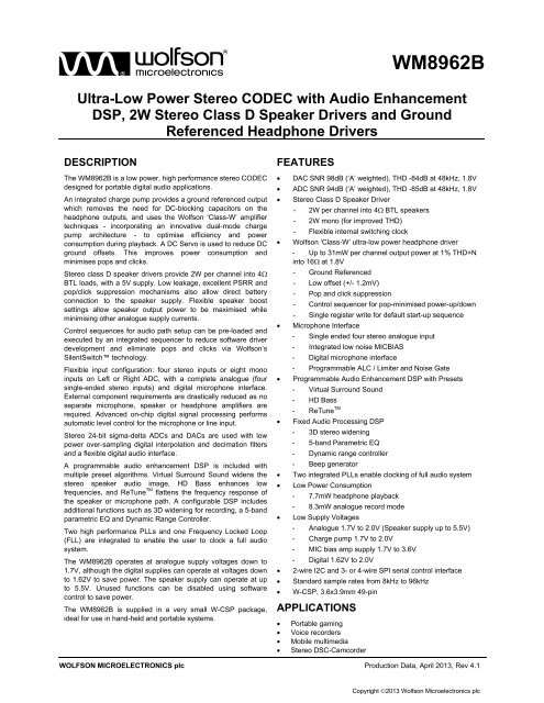
Production DataDEVICE DESCRIPTIONINTRODUCTION<strong>WM8962B</strong>The <strong>WM8962B</strong> is a low power audio CODEC offering a combination of high quality audio, advancedfeatures, low power and small size. These characteristics make it ideal for portable digital audioapplications with stereo speaker and headphone outputs such as games consoles, portable mediaplayers and multimedia phones.A flexible input configuration supports a single-ended stereo microphone interface and a digitalmicrophone interface. A boost amplifier is available for additional gain on the microphone inputs. Aprogrammable gain amplifier (PGA) with an automatic level control (ALC) function can be used tomaintain a constant microphone recording volume.Stereo class D speaker drivers can provide up to 2W per channel into 4 BTL loads. It is alsopossible to configure the speaker drivers as a mono output, giving enhanced performance.Highly flexible output speaker boost settings provide fully internal level-shifting of analogue outputsignals, allowing speaker output power to be maximised while minimising other analogue supplycurrents, and requiring no additional components.A dual mode (Level Shifting or Inverting Mode) charge pump generates split supplies for theheadphone output amplifiers allowing these to be ground referenced.A DC servo to remove offsets from the headphone outputs, low leakage and a user controlled powerup/power-downControl Sequencer provides powerful pop and click suppression mechanisms whichenable direct battery connection. These anti-pop/click mechanisms, and no requirement for anyexternal DC blocking capacitors to the headphone, result in a reduced external component count andreduced power consumption in portable battery-powered applications.The hi-fi quality stereo ADC and DAC uses a 24-bit, low-order over-sampling architecture to deliveroptimum performance. ADC and DAC operate at the same sample rate.An audio enhancement DSP provides powerful benefits in audio processing. Three algorithms arepre-programmed in the DSP. ReTune TMflattens the frequency response of the full record and/orplayback path, including microphone, speaker and housing. Virtual Surround Sound widens the stereospeaker audio image. High Definition Bass enhances low frequencies, improving the performance ofsmall speakers. Further audio enhancements are provided in a fix function DSP – 3D enhancement, a5-band parametric equaliser, and a Dynamic Range Controller.The <strong>WM8962B</strong> has a highly flexible digital audio interface, supporting a number of protocols, includingI2S, DSP, MSB-first left/right justified, and can operate in master or slave modes. PCM operation issupported in the DSP mode. A-law and -law companding are also supported. Time divisionmultiplexing (TDM) is available to allow multiple devices to stream data simultaneously on the samebus, saving space and power.The <strong>WM8962B</strong> provides two integrated PLLs and one FLL to generate internal and external clocksignals. The SYSCLK (internal system clock) provides clocking for all internal functions. SYSCLK canbe derived directly from the MCLK pin, or else using one of the PLLs or the FLL. All MCLKfrequencies typically used in portable systems are supported for sample rates between 8 kHz and 96kHz. The ADC and DAC must be configured to operate at the same sample rate. A flexible switchingclock for the class D speaker drivers (synchronous with the audio DSP clocks for best performance) isalso derived from SYSCLK.To allow full software control over all its features, the <strong>WM8962B</strong> supports 2-wire (I2C) and 3- or 4-wire(SPI) serial control interface modes, with full read-back capability on all registers. The <strong>WM8962B</strong> isfully compatible with, and an ideal partner to, a wide range of industry standard microprocessors,controllers and DSPs. Unused functions can be disabled via software to save power, while lowleakage currents extend standby and off time in portable battery-powered applications.wPD, April 2013, <strong>Rev</strong> <strong>4.1</strong>37
Production DataINPUT SIGNAL PATH<strong>WM8962B</strong>The <strong>WM8962B</strong> has many analogue input channels, configurable in combinations of up to eight monoinputs or four stereo inputs.Any of the analogue inputs may be connected to the input PGA on the associated left or right channel.(Note that only one analogue input can be connected to the PGA at any time; the PGA does notperform any signal mixing.)The left and right analogue inputs IN2 and IN3 can be connected to the input boost mixer on theassociated left or right channel, bypassing the input PGA.Note that the input signal path audio performance is affected by the choice of signal path. Bestperformance is achieved using analogue inputs IN2 or IN3 connected directly to the input boost mixer.The performance of the input signal paths are ranked as described in the list below (best performancefirst).IN2 or IN3 connected directly to the input boost mixerIN1 or IN4 connected via the input PGAIN2 or IN3 connected via the input PGAThe left and right analogue inputs IN4 can be connected directly to the output signal mixers, whichdrive the headphone or speaker outputs.The input signal paths and the control registers are shown in Figure 13.To Left and Right Speakerand Headphone MixersIN1LIN4LIN2LIN3LIN1L_TO_INPGALIN4L_TO_INPGALIN2L_TO_INPGALIN3L_TO_INPGALVMIDIN2L_TO_MIXINL / IN2L_MIXINL_VOLMIXINLPGALIN3L_TO_MIXINL / IN3L_MIXINL_VOL+INPGAL_TO_MIXINL / INPGAL_MIXINL_VOL+MIXINL_ENAINPGAL_ENAororINL_ENAINL_ENAMIXINL_MUTEINL_VOLIN_VUINL_ZCINPGAL_MUTEADCADCDIGITALFILTERSALCIN1RIN4RIN2RIN1R_TO_INPGARIN4R_TO_INPGARIN2R_TO_INPGARINPGAR_ENAorINR_ENAINR_VOLIN_VUINR_ZCINPGAR_MUTEPGARINPGAR_TO_MIXINR / INPGAR_MIXINR_VOL+IN3R_TO_MIXINR / IN3R_MIXINR_VOLIN2R_TO_MIXINR / IN2R_MIXINR_VOLMIXINR+ADCWind noiseFilterVolumeIN3RIN3R_TO_INPGARVMIDMIXINR_ENAorINR_ENAMIXINR_MUTETo Left and Right Speakerand Headphone MixersFigure 13 Analogue Input Signal PathwPD, April 2013, <strong>Rev</strong> <strong>4.1</strong>38
Production DataMICROPHONE INPUT CONNECTION<strong>WM8962B</strong>The <strong>WM8962B</strong> supports analogue and digital microphone input. Refer to the “Digital MicrophoneInterface” section for details of the digital microphone input.The input PGAs can support a single-ended analogue microphone input. A microphone bias generatoris also provided, suitable for powering electret condenser microphones.Single-ended analogue microphone input using IN1L, IN1R, IN4L or IN4R is configured as shown inFigure 14.Figure 14 Microphone Input IN1 or IN4When using IN2L, IN2R, IN3L or IN3R as an input to the PGA, the respective IN1 pin (IN1L or IN1R)must be connected to ground via an external capacitor, as shown in Figure 15.Note that when IN2L, IN2R, IN3L or IN3R is selected as input to the PGA (using the register bitsdescribed in Table 6), the respective IN1 pin (IN1L or IN1R) is automatically connected to the PGA inorder to support the capacitor requirement described above.Figure 15 Microphone Input IN2 or IN3LINE INPUT CONNECTIONSingle-ended line inputs may be connected to the left or right channel analogue inputs IN1, IN2, IN3or IN4, and routed to the input mixers or output signal paths as illustrated in Figure 14.If IN2L, IN2R, IN3L or IN3R is used as an input to the PGA, then the respective IN1 pin (IN1L or IN1R)must be connected to ground via an external capacitor, as shown in Figure 15.Note that when IN2L, IN2R, IN3L or IN3R is selected as input to the PGA (using the register bitsdescribed in Table 6), the respective IN1 pin (IN1L or IN1R) is automatically connected to the PGA inorder to support the capacitor requirement described above.wPD, April 2013, <strong>Rev</strong> <strong>4.1</strong>39
Production Data<strong>WM8962B</strong>MICROPHONE BIAS CONTROLThere is one MICBIAS generator which provides low noise reference voltages suitable for biasingelectret condenser (ECM) type microphones via an external resistor.Note that an external decoupling capacitor is required on the MICBIAS output. A suitable capacitormust be connected whenever the MICBIAS output is enabled. Additional filtering of the MICBIASoutput, to reduce noise and interference, may be implemented as described in the “ApplicationsInformation” section, if required.The MICBIAS output is enabled using the MICBIAS_ENA register bit. The MICBIAS voltage isselected using the MICBIAS_LVL and MICBIAS_EVR register fields, as detailed in Table 2.REGISTERADDRESSR25 (19h)Pwr Mgmt(1)R29 (1Dh)Pwr Mgmt(3)R48 (30h)MICBIASBIT LABEL DEFAULT DESCRIPTION1 MICBIAS_ENA 0 Microphone Bias Enable0 = OFF (high impedance output)1 = ON1:0 MICBIAS_EVR[1:0]00 Microphone Bias Voltage Control00 = Controlled by MICBIAS_LVL01 = 1.63 x AVDD (approx.)10 = 1.34 x AVDD (approx.)11 = 1.63 x AVDD (approx.)0 MICBIAS_LVL 1 Microphone Bias Voltage Control0 = 0.828 x AVDD (approx.)1 = 1.156 x AVDD (approx.)Only valid when MICBIAS_EVR=00. Inother cases, the Microphone Bias voltageis controlled by MICBIAS_EVR alone.Table 2 Microphone Bias ControlNote that the maximum source current capability for MICBIAS is 2.0mA. The external biasingresistance must be large enough to limit the MICBIAS current to 2.0mA across the full microphoneimpedance range.Note that the MICVDD supply voltage must be at least 300mV higher than the desired MICBIASoutput voltage.MICBIAS CURRENT DETECTA MICBIAS Current Detect function is provided for external accessory detection. This is provided inorder to detect the insertion/removal of a microphone or the pressing/releasing of the microphone‘hook’ switch; these events will cause a significant change in MICBIAS current flow, which can bedetected and used to generate a signal to the host processor.The MICBIAS current detect function is enabled by setting the MICDET_ENA register bit. When thisfunction is enabled, two current thresholds can be defined, using the MICDET_THR andMICSHORT_THR registers. When a change in MICBIAS current which crosses either threshold isdetected, then an interrupt event can be generated. In a typical application, accessory insertion wouldbe detected when the MICBIAS current exceeds MICDET_THR, and microphone hookswitchoperation would be detected when the MICBIAS current exceeds MICSHORT_THR.The current detect threshold functions are both inputs to the Interrupt control circuit and can be usedto trigger an Interrupt event when either threshold is crossed. Both events can also be indicated as anoutput on a GPIO pin - see “General Purpose Input/Output (GPIO)”. The status flags MICDET_STS orMICSHORT_STS are also asserted whenever the relevant current threshold is exceeded.The current detect thresholds are enabled and controlled using the registers described in Table 3Performance parameters for this circuit block can be found in the “Electrical Characteristics” section.Filtering is also provided in both current detect circuits to improve reliability in conditions where ACcurrent spikes are present due to ambient noise conditions. This feature is described in the followingsection. Further guidance on the usage of the MICBIAS current monitoring features is also describedin the following pages.wPD, April 2013, <strong>Rev</strong> <strong>4.1</strong>40
Production Data<strong>WM8962B</strong>REGISTERADDRESSR48 (30h)AdditionalControl (4)BIT LABEL DEFAULT DESCRIPTION14:12 MICDET_THR [2:0] 000 MICBIAS Current Detect Threshold(AVDD = 1.8V)000 = 64uA001 = 166uA010 = 375uA011 = 475uA100 = 575uA101 = 680uA110 = 885uA111 = 990uANote that the value scales withAVDD. The value quoted is correctfor AVDD=1.8V.11:10 MICSHORT_THR [1:0] 00 MICBIAS Short Circuit Threshold(AVDD = 1.8V)00 = 515uA01 = 680uA10 = 1050uA11 = 1215uANote that the value scales withAVDD. The value quoted is correctfor AVDD=1.8V.9 MICDET_ENA 0 MICBIAS Current and Short CircuitDetect Enable0 = Disabled1 = Enabled7 MICDET_STS 0 MICBIAS Current Detection status0 = Current Detect threshold notexceeded1 = Current Detect thresholdexceeded6 MICSHORT_STS 0 MICBIAS Short Circuit status0 = Short Circuit threshold notexceeded1 = Short Circuit thresholdexceededTable 3 MICBIAS Current DetectMICBIAS CURRENT DETECT FILTERINGThe function of the filtering is to ensure that AC current spikes caused by ambient noise conditionsnear the microphone do not lead to incorrect signalling of the microphone insertion/removal status orthe microphone hookswitch status.Digital filtering of the hookswitch status ensures that the MICBIAS Short Circuit detection event is onlysignalled if the MICSHORT_THR threshold condition has been met for 10 consecutive measurements.In a typical application, microphone insertion would be detected when the MICBIAS current exceedsthe Current Detect threshold set by MICDET_THR.When the MICD_IRQ_POL interrupt polarity bit is set to 0, then microphone insertion detection willcause the MICD_EINT interrupt status register to be set. (See “Interrupts” for details of these registerbits.)For detection of microphone removal, the MICD_IRQ_POL bit should be set to 1. When theMICD_IRQ_POL interrupt polarity bit is set to 1, then microphone removal detection will cause theMICD_EINT interrupt status register to be set.wPD, April 2013, <strong>Rev</strong> <strong>4.1</strong>41
Production Data<strong>WM8962B</strong>The detection of these events is bandwidth limited for best noise rejection, and is subject to detectiondelay time t DET , as specified in the “Electrical Characteristics” section. Provided that the MICDET_THRfield has been set appropriately, each insertion or removal event is guaranteed to be detected withinthe delay time t DET .It is likely that the microphone socket contacts will have mechanical “bounce” when a microphone isinserted or removed, and hence the resultant control signal will not be a clean logic level transition.Since t DET has a range of values, it is possible that the interrupt will be generated before themechanical “bounce” has ceased. Hence after a mic insertion or removal has been detected, a timedelay should be applied before re-configuring the MICD_IRQ_POL bit. The maximum possiblemechanical bounce times for mic insertion and removal must be understood by the softwareprogrammer.Utilising a GPIO pin to monitor the steady state of the microphone detection function does not changethe timing of the detection mechanism, so there will also be a delay t DET before the signal changesstate. It may be desirable to implement de-bounce in the host processor when monitoring the state ofthe GPIO signal.Microphone hook switch operation is detected when the MICBIAS current exceeds the Short CircuitDetect threshold set by MICSHORT_THR. Using the digital filtering, the hook switch detection event isonly signalled if the MICSHORT_THR threshold condition has been met for 10 consecutivemeasurements.When the MICSCD_IRQ_POL interrupt polarity bit is set to 0, then hook switch operation will causethe MICSCD_EINT interrupt status register to be set. (See “Interrupts” for details of these registerbits.)For detection of microphone removal, the MICSCD_IRQ_POL bit should be set to 1. When theMICSCD_IRQ_POL interrupt polarity bit is set to 1, then hook switch release will cause theMICSCD_EINT interrupt status register to be set.The hook switch detection measurement frequency and the detection delay time t SHORT are detailed inthe “Electrical Characteristics” section.The <strong>WM8962B</strong> Interrupt function is described in the “Interrupts” section. Example control sequencesfor configuring the Interrupts functions for MICBIAS current detection events are described in the“Applications Information” section.A clock is required for the digital filtering function. This requires:MCLK is present or the FLL is selected as the SYSCLK source in free-running mode SYSCLK_ENA = 1Any MICBIAS Current Detect event (accessory insertion/removal or hookswitch press/release) whichhappens while one or more of the clocking criteria is not satisfied (for example during a low powermode where the CPU has disabled MCLK) will still be detected, but only after the clocking conditionsare met. An example is illustrated in Figure 16, where the mic is inserted while MCLK is stopped.Note that the interrupts and digital filtering can be supported in the absence of an external clock byusing the FLL in free-running mode and selecting the FLL as the clock source, as described in“Clocking and Sample Rates”.wPD, April 2013, <strong>Rev</strong> <strong>4.1</strong>42
Production Data<strong>WM8962B</strong>Figure 16 MICBIAS Detection Events without MCLKMICROPHONE HOOK SWITCH DETECTIONThe possibility of spurious hook switch interrupts due to ambient noise conditions can be removed bydetailed understanding of microphone behaviour under extremely high sound pressure levels orduring mechanical shock, and by correct selection of the MICBIAS resistor value; these factors willaffect the level of the MICBIAS AC current spikes.In applications where the Current Detect threshold is close to the level of the current spikes, theprobability of false detections is reduced by the digital filtering described above.Note that the filtering algorithm provides only limited rejection of very high current spikes atfrequencies less than or equal to the hook switch detect measurement frequency, or at frequenciesequal to harmonics of the hook switch detect measurement frequency.The MICBIAS Hook Switch detection filtering is illustrated in Figure 17. Example control sequences forconfiguring the Interrupts functions for MICBIAS current detection events are described in the“Applications Information” section.Figure 17 MICBIAS Hook Switch Detection FilteringwPD, April 2013, <strong>Rev</strong> <strong>4.1</strong>43
Production Data<strong>WM8962B</strong>MULTIPLE PUSH BUTTON DETECTIONThe MICDET_THR and MICSHORT_THR current detection thresholds can be used to detectaccessory insertion and hook switch status as described above. The <strong>WM8962B</strong> can also beconfigured to support multiple button detection, as illustrated in Figure 18.Multiple push button detection is supported using carefully chosen resistors to distinguish one pushbutton from another, and by using the <strong>WM8962B</strong> Analogue to Digital Converter (ADC) to measure thepotential divider formed between the MICBIAS resistor and the push button resistors.The push buttons are connected in parallel, each with a uniquely-valued series resistor. Assertion ofany of the push buttons will result in a different voltage measurement, depending on which button hasbeen pressed.The resistor values must be carefully selected to ensure that each push button can be reliably anduniquely recognised. It must also be ensured that the DC connection (to pin IN4L as illustrated inFigure 18) does not exceed the maximum input voltage for that pin. Note that the MICBIAS voltagemay need to be reduced as a result.In order to meet the maximum input voltage limit described above, it is required thatMICBIAS_EVR=00 under the circuit configuration shown.Note that the IN1L and IN4L input paths should not be enabled simultaneously as inputs to the PGA.As a result, it should be noted that the microphone/line audio input path to the PGA cannot besupported at the same time as DC measurement via the same PGA.In a typical application, the MICBIAS short circuit detect feature should be used to detect a pushbutton operation in the first instance. When this event has been detected, then IN1L should bedisabled, and IN4L should then be enabled to allow the ADC measurement to determine which buttonhas been pressed.The push button detection mechanism described here can be implemented using the IN4L pin or theIN4R pin. It is not recommended to use any other input pin for push button detection.When using the DC voltage measurement function, the IN4 pins must be configured using the registersequence described in Table 4, in order to disconnect these pins from the internal voltage reference.REGISTER ADDRESSVALUEFDh0002hCCh0040hFDh0000hTable 4 Input Pins IN4L and IN4R Configuration for Push Button DetectionWhen using the ADC to perform DC voltage measurement for push button detection, the ADC HighPass Filter must be disabled. See “ADC Signal Path Enhancements” for details of the ADC_HPF_DISregister bit to control this filter. It is recommended to set the PGA gain to 0dB for DC measurement.wPD, April 2013, <strong>Rev</strong> <strong>4.1</strong>44
Production Data<strong>WM8962B</strong>Figure 18 Multiple Hook Switch DetectionINPUT PGA ENABLEThe <strong>WM8962B</strong> has two input PGAs (Programmable Gain Amplifiers), which provide adjustable gainon the applicable input signal paths.The input PGAs are enabled using register bits INL_ENA, INR_ENA, INPGAR_ENA andINPGAL_ENA, as described in Table 5.REGISTERADDRESSR25 (19h)Pwr Mgmt (1)R37 (25h)Left Input PGAControlR38 (26h)Right InputPGA ControlTable 5 Input PGA EnableBIT LABEL DEFAULT DESCRIPTION5 INL_ENA 0 Left Input PGA and Mixer Enable.0 = Disabled1 = Enabled4 INR_ENA 0 Right Input PGA and Mixer Enable.0 = Disabled1 = Enabled4 INPGAL_ENA 0 Left Input PGA Enable0 = Disabled1 = EnabledNote that the Left Input PGA is alsoenabled when INL_ENA is set4 INPGAR_ENA 0 Right Input PGA Enable0 = Disabled1 = EnabledNote that the Right Input PGA isalso enabled when INR_ENA is setTo enable the input PGAs, the reference voltage VMID and the bias current must also be enabled.See “Reference Voltages and Bias Control” for details of the associated controls VMID_SEL andBIAS_ENA.wPD, April 2013, <strong>Rev</strong> <strong>4.1</strong>45
Production Data<strong>WM8962B</strong>INPUT PGA CONFIGURATIONEach of the PGAs operates in a single-ended mode. Configuration of the PGA inputs to the <strong>WM8962B</strong>input pins is controlled using the register bits shown in Table 6.The maximum available attenuation on any of these input paths is achieved by using register bitsshown in Table 6 to disconnect the input pins from the applicable PGA.REGISTERADDRESSR37 (25h)Left inputPGA controlR38 (26h)Right inputPGA controlBIT LABEL DEFAULT DESCRIPTION3 IN1L_TO_INPGAL 1 Selects the IN1L pin as an input to theLeft PGA0 = Disabled1 = Enabled2 IN2L_TO_INPGAL 0 Selects the IN2L pin as an input to theLeft PGA0 = Disabled1 = Enabled1 IN3L_TO_INPGAL 0 Selects the IN3L pin as an input to theLeft PGA0 = Disabled1 = Enabled0 IN4L_TO_INPGAL 0 Selects the IN4L pin as an input to theLeft PGA0 = Disabled1 = Enabled3 IN1R_TO_INPGAR2 IN2R_TO_INPGAR1 IN3R_TO_INPGAR0 IN4R_TO_INPGARTable 6 Input PGA Configuration1 Selects the IN1R pin as an input to theRight PGA0 = Disabled1 = Enabled0 Selects the IN2R pin as an input to theRight PGA0 = Disabled1 = Enabled0 Selects the IN3R pin as an input to theRight PGA0 = Disabled1 = Enabled0 Selects the IN4R pin as an input to theRight PGA0 = Disabled1 = EnabledwPD, April 2013, <strong>Rev</strong> <strong>4.1</strong>46
Production Data<strong>WM8962B</strong>INPUT PGA VOLUME CONTROLEach of the two Input PGAs has an independently controlled gain range of -23.25dB to +24dB in0.75dB steps. Each Input PGA can be independently muted using the PGA mute bits as described inTable 7, with maximum mute attenuation achieved by simultaneously disabling the correspondinginputs described in Table 6.To prevent "zipper noise", a zero-cross function is provided on the input paths. When this feature isenabled, volume updates will not take place until a zero-crossing is detected. In the case of a longperiod without zero-crossings, a timeout function is provided. When the zero-cross function isenabled, the volume will update after the timeout period if no earlier zero-cross has occurred. Thetimeout clock is enabled using TOCLK_ENA, the timeout period is set by TOCLK_DIV. See “Clockingand Sample Rates” for more information on these fields.The IN_VU bits control the loading of the input PGA volume data and the PGA mute functions. WhenIN_VU is set to 0, the PGA volume data will be loaded into the respective control register, but will notactually change the gain setting. The INL and INR volume settings are both updated when a 1 iswritten to either IN_VU bit. Similarly, the INPGAL_MUTE and INPGAR_MUTE settings are onlyeffective when a 1 is written to either IN_VU bit. This makes it possible to update the gain/mute of theleft and right signal paths simultaneously.Note that the Input PGA control has a dependency on the correct sequencing of the ALC and ADCEnable control registers; if the correct sequences are not followed, then the Input PGA gain settingsmay become fixed. See “Automatic Level Control (ALC)” for further details.The Input PGA Volume Control register fields are described in Table 7 and Table 8.REGISTERADDRESSR0 (0h)Left inputvolumeR1 (1h)Right inputvolumeBIT LABEL DEFAULT DESCRIPTION8 IN_VU N/A Input PGA Volume and Mute UpdateWriting a 1 to this bit will cause the INLand INR volume and mute settings to beupdated simultaneously7 INPGAL_MUTE1 Left input PGA Mute0 = Unmuted1 = Muted6 INL_ZC 0 INL PGA Zero Cross Detector0 = Change gain immediately1 = Change gain on zero cross only5:0 INL_VOL[5:0]011111(0dB)Left input PGA Volume-23.25dB to +24.00dB in 0.75dB steps.See Table 8 for volume range.8 IN_VU N/A Input PGA Volume and Mute UpdateWriting a 1 to this bit will cause the INLand INR volume and mute settings to beupdated simultaneously7 INPGAR_MUTE1 Right input PGA Mute0 = Unmuted1 = Muted6 INR_ZC 0 INR PGA Zero Cross Detector0 = Change gain immediately1 = Change gain on zero cross only5:0 INR_VOL[5:0]Table 7 Input PGA Volume Control01_1111(0dB)Right input PGA Volume-23.25dB to +24.00dB in 0.75dB steps.See Table 8 for volume range.wPD, April 2013, <strong>Rev</strong> <strong>4.1</strong>47
Production Data<strong>WM8962B</strong>INL_VOL[5:0], INR_VOL[5:0]VOLUME(dB)INL_VOL[5:0], INR_VOL[5:0]VOLUME(dB)00_0000 -23.25 10_0000 0.7500_0001 -22.50 10_0001 1.5000_0010 -21.75 10_0010 2.2500_0011 -21.00 10_0011 3.0000_0100 -20.25 10_0100 3.7500_0101 -19.50 10_0101 4.5000_0110 -18.75 10_0110 5.2500_0111 -18.00 10_0111 6.0000_1000 -17.25 10_1000 6.7500_1001 -16.50 10_1001 7.5000_1010 -15.75 10_1010 8.2500_1011 -15.00 10_1011 9.0000_1100 -14.25 10_1100 9.7500_1101 -13.50 10_1101 10.5000_1110 -12.75 10_1110 11.2500_1111 -12.00 10_1111 12.0001_0000 -11.25 11_0000 12.7501_0001 -10.50 11_0001 13.5001_0010 -9.75 11_0010 14.2501_0011 -9.00 11_0011 15.0001_0100 -8.25 11_0100 15.7501_0101 -7.50 11_0101 16.5001_0110 -6.75 11_0110 17.2501_0111 -6.00 11_0111 18.0001_1000 -5.25 11_1000 18.7501_1001 -4.50 11_1001 19.5001_1010 -3.75 11_1010 20.2501_1011 -3.00 11_1011 21.0001_1100 -2.25 11_1100 21.7501_1101 -1.50 11_1101 22.5001_1110 -0.75 11_1110 23.2501_1111 0.00 11_1111 24.00Table 8 Input PGA Volume RangewPD, April 2013, <strong>Rev</strong> <strong>4.1</strong>48
Production Data<strong>WM8962B</strong>INPUT MIXER ENABLEThe <strong>WM8962B</strong> has two analogue input mixers, which provide mixing and signal boost functions forthe analogue input paths.The input mixers MIXINL and MIXINR are enabled by the MIXINL_ENA and MIXINR_ENA registerbits, as described in Table 9. Note that the input mixers can also be controlled by INL_ENA andINR_ENA, as described in Table 5.REGISTERADDRESSR31 (1Fh)Input mixercontrol (1)Table 9 Input Mixer EnableBIT LABEL DEFAULT DESCRIPTION1 MIXINL_ENA 0 Left Input Mixer Enable0 = Disabled1 = EnabledNote that the Left Input Mixer is alsoenabled when INL_ENA is set0 MIXINR_ENA 0 Right Input Mixer Enable0 = Disabled1 = EnabledNote that the Right Input Mixer is alsoenabled when INR_ENA is setINPUT MIXER CONFIGURATION AND VOLUME CONTROLThe analogue input mixers MIXINL and MIXINR can be configured to take input from the input PGAsand also directly from the IN2 and IN3 inputs pins.The Input Boost Mixer configuration and volume controls are described in Table 10 for the Left inputboost-mixer (MIXINL) and Table 11 for the Right input boost-mixer (MIXINR).Note that the available mixer gain settings for the IN2 and IN3 paths are different to the input PGAsignal paths. The IN2 and IN3 signal paths can be controlled from -12dB to +6dB. The input PGAsignal paths can be controlled from 0dB to +29dB.To prevent pop noise, it is recommended that gain and mute controls for the input boost mixers arenot modified while the signal paths are active. If volume control is required on these signal paths, it isrecommended that this is implemented using the input PGA volume controls or the ADC volumecontrols. The ADC volume controls are described in the “Analogue To Digital Converter (ADC)”section.REGISTERADDRESSR31 (1Fh)Input mixercontrol (1)R32 (20h)Left inputmixervolumeBIT LABEL DEFAULT DESCRIPTION3 MIXINL_MUTE 0 Left input boost-mixer mute0 = Un-mute1 = Mute8:6 IN2L_MIXINL_VOL [2:0] 101 Left input IN2L to Left inputBoost-Mixer Gain000 = -12dB001 = -12dB010 = -9dB011 = -6dB100 = -3dB101 = 0dB110 = +3dB111 = +6dBwPD, April 2013, <strong>Rev</strong> <strong>4.1</strong>49
Production Data<strong>WM8962B</strong>REGISTERADDRESSR34 (22h)Input mixercontrol (2)BIT LABEL DEFAULT DESCRIPTION5:3 INPGAL_MIXINL_VOL[2:0]000 Left input PGA to Left inputBoost-Mixer Gain000 = 0dB001 = +6dB010 = +13dB011 = +18dB100 = +20dB101 = +24dB110 = +27dB111 = +29dB2:0 IN3L_MIXINL_VOL [2:0] 101 Left input IN3L to Left inputBoost-Mixer Gain000 = -12dB001 = -12dB010 = -9dB011 = -6dB100 = -3dB101 = 0dB110 = +3dB111 = +6dB5 IN2L_TO_MIXINL 0 Left Input IN2L to Left inputBoost-Mixer Select0 = Disabled1 = Enabled4 IN3L_TO_MIXINL 0 Left Input IN3L to Left inputBoost-Mixer Select0 = Disabled1 = Enabled3 INPGAL_TO_MIXINL 1 Left Input PGA to Left inputBoost-Mixer Select0 = Disabled1 = EnabledTable 10 Left Input Mixer (MIXINL) Volume ControlREGISTERADDRESSR31 (1Fh)Input mixercontrol (1)R33 (21h)Right inputmixervolumeBIT LABEL DEFAULT DESCRIPTION2 MIXINR_MUTE 0 Right input boost-mixer mute0 = Un-mute1 = Mute8:6 IN2R_MIXINR_VOL[2:0]101 Right input IN2R to Right inputBoost-Mixer Gain000 = -12dB001 = -12dB010 = -9dB011 = -6dB100 = -3dB101 = 0dB110 = +3dB111 = +6dBwPD, April 2013, <strong>Rev</strong> <strong>4.1</strong>50
Production Data<strong>WM8962B</strong>REGISTERADDRESSR34 (22h)Input mixercontrol (2)BIT LABEL DEFAULT DESCRIPTION5:3 INPGAR_MIXINR_VOL[2:0]2:0 IN3R_MIXINR_VOL[2:0]000 Right input PGA to Right inputBoost-Mixer Gain000 = 0dB001 = +6dB010 = +13dB011 = +18dB100 = +20dB101 = +24dB110 = +27dB111 = +29dB101 Right input IN3R to Right inputBoost-Mixer Gain000 = -12dB001 = -12dB010 = -9dB011 = -6dB100 = -3dB101 = 0dB110 = +3dB111 = +6dB2 IN2R_TO_MIXINR 0 Right input IN2R to Right inputBoost-Mixer Select0 = Disabled1 = Enabled1 IN3R_TO_MIXINR 0 Right input IN3R to Right inputBoost-Mixer Select0 = Disabled1 = Enabled0 INPGAR_TO_MIXINR 1 Right input PGA to Right inputBoost-Mixer Select0 = Disabled1 = EnabledTable 11 Right Input Mixer (MIXINR) Volume ControlwPD, April 2013, <strong>Rev</strong> <strong>4.1</strong>51
Production DataAUTOMATIC LEVEL CONTROL (ALC)<strong>WM8962B</strong>The <strong>WM8962B</strong> has an automatic PGA gain control circuit that keeps a constant recording volumeirrespective of the input signal level. This is achieved by continuously adjusting the input PGA gain sothat the signal level at the ADC input remains constant.A digital peak detector monitors the ADC output and changes the PGA gain if necessary.The ALC has two modes selected by the ALC_MODE register. See the “Limiter Mode” section forfurther details on the ALC Modes.The ALC also has a Noise Gate function, which provides additional control of low level input signals.This means that the signal path is quiet when no signal is present, giving an improvement inbackground noise level.The Automatic Level Control (ALC) can be enabled on either the left channel, or the right channel, oron both channels, using the ALCL_ENA and ALCR_ENA fields respectively. Note that the ALC (Left)function requires the Left and Right ADCs to be enabled; the ALC (Right) function only requires theRight ADC to be enabled.Note that, when disabling the input signal path, the ALC must be disabled before the respective ADCsare disabled. If this sequence is not followed, then the Input PGA gain settings may become fixed.The ALC should not be enabled when using the IN2 or IN3 inputs connected directly to the input boostmixer; this is because these paths will bypass the PGAs where the ALC gain adjustment is performed.ALC can be set to Active Mode or to Monitor Mode. When ALC is in Active Mode(ALC_INACTIVE_ENA = 0), the gain of the analogue PGAs is controlled by the ALC bit settings, andnot by the INL_VOL or the INR_VOL fields. When ALC is in Monitor Mode (ALC_INACTIVE_ENA=1),ALC monitors the signal levels without doing any of the level control that it would otherwise perform.Details on readback of the ALC status are in the “ALC Status Readback” section.When the ALC is enabled, a target level for the analogue input signal at the ADC is determined by theALC_LVL setting. There are two ranges (high or low) from which the ALC_LVL target value can betaken. The target values in each of these ranges are shown in Table 13. Two ranges can be selectedusing ALC_LVL_MODE. Set ALC_LVL_MODE to 0 to use the low range (-28.5dBFS to -6dBFS), orset ALC_LVL_MODE to 1 to use the higher range (-22.5dBFS to -1.5dBFS).wPD, April 2013, <strong>Rev</strong> <strong>4.1</strong>52
Production Data<strong>WM8962B</strong>REGISTERADDRESSR17 (11h)ALC1BIT LABEL DEFAULT DESCRIPTION10 ALC_INACTIVE_ENA 0 Select whether the ALC is in ActiveMode (that is, ALC is controlling thePGA gain) or in Monitor Mode (theanalogue controls are disabled). Notethat at least one of ALCL_ENA andALCR_ENA must also be enabled0 = ALC is in Active Mode1 = ALC is in Monitor Mode9 ALC_LVL_MODE 0 Select the range of the ALC targetlevel.0 = -28.5dBFS to -6dBFS in 1.5dBsteps1 = -22.5dBFS to -1.5dBFS in 1.5dBsteps8 ALCL_ENA 0 Select ALC on the Left channel0 = Disabled (PGA gain set byINL_VOL)1 = EnabledNote that in stereo mode, the left andright PGA volumes, and left and rightboost mixer volumes, must be thesame before setting ALCL_ENA = 1and ALCR_ENA = 17 ALCR_ENA 0 Select ALC on the Right channel0 = Disabled (PGA gain set byINR_VOL)1 = EnabledNote that in stereo mode, the left andright PGA volumes, and left and rightboost mixer volumes, must be thesame before setting ALCL_ENA = 1and ALCR_ENA = 13:0 ALC_LVL [3:0] 1011 Set the Target signal level at theADC input.Note that the target level is alsodetermined by ALC_LVL_MODE.ALC_LVL_MODE = 00000 = -28.5dBFS0001 = -27.0dBFS…in 1.5dB steps to…1111 = -6dBFSALC_LVL_MODE = 10000 = -22.5dBFS0001 = -21.0dBFS…in 1.5dB steps to…1110 = -1.5dBFS1111 = -1.5dBFSTable 12 Automatic Level ControlSee Table 13 for the range ofpossible values.wPD, April 2013, <strong>Rev</strong> <strong>4.1</strong>53
Production Data<strong>WM8962B</strong>ALC_LVL ALC_LVL_MODE = 0(dBFS)ALC_LVL_MODE = 1(dBFS)0000 -28.5 -22.50001 -27.0 -21.00010 -25.5 -19.50011 -24.0 -18.00100 -22.5 -16.50101 -21.0 -15.00110 -19.5 -13.50111 -18.0 -12.01000 -16.5 -10.51001 -15.0 -9.01010 -13.5 -7.51011 -12.0 -6.01100 -10.5 -4.51101 -9.0 -3.01110 -7.5 -1.51111 -6.0 -1.5Table 13 ALC Target Level ValuesLIMITER MODEIn Normal Mode (ALC_MODE = 0), the ALC will attempt to maintain a constant signal level byincreasing or decreasing the gain of the PGA. This is illustrated in Figure 19.In Limiter Mode (ALC_MODE = 1), the ALC will reduce peaks that go above the threshold level, butwill not increase the PGA gain beyond the starting level. (The starting level is defined as the gainsetting of the PGA at the time when the ALC is enabled.) This is illustrated in Figure 20.Note that ALC_MODE should not be changed while the ALC is active. ALCL_ENA and ALCR_ENAmust both be set to 0 before changing ALC_MODE.REGISTERADDRESSR19 (13h)ALC3BIT LABEL DEFAULT DESCRIPTION8 ALC_MODE 0 ALC Mode0 = Normal ALC Mode1 = Limiter ModeNote that ALCL_ENA andALCR_ENA must both be set to 0before changing ALC_MODE,otherwise unexpected behaviourmay result.Table 14 ALC Mode Switch (ALC_MODE)wPD, April 2013, <strong>Rev</strong> <strong>4.1</strong>54
Production Data<strong>WM8962B</strong>Figure 19 ALC Normal Mode OperationFigure 20 ALC Limiter Mode OperationwPD, April 2013, <strong>Rev</strong> <strong>4.1</strong>55
Production Data<strong>WM8962B</strong>ALC GAIN CONTROLThe minimum and maximum gain applied by the ALC is set by register fields ALC_MINGAIN andALC_MAXGAIN respectively. These limits can be used to alter the ALC response from that illustratedin Figure 19 and Figure 20. If the range between maximum and minimum gain is reduced, then theextent of the automatic level control is reduced.Note that, when the ALC is first enabled, the PGA gain (in dB) must be less than the ALC_MAXGAINsetting. The PGA gain is controlled by the INL_VOL and INR_VOL registers, as described in Table 7.The minimum gain in the ALC response is set by ALC_MINGAIN. The minimum gain limit can be usedto prevent excessive attenuation of the signal path.The maximum gain limit set by ALC_MAXGAIN can be used to prevent quiet signals (or silence) frombeing excessively amplified. Note that the Noise Gate function also affects quiet signals. See the “ALCNoise Gate” section (below) for further details on the Noise Gate.To prevent "zipper noise", a zero-cross function is provided within the ALC. When this feature isenabled, volume updates will not take place until a zero-crossing is detected. In the case of a longperiod without zero-crossings, a timeout function is provided. When the zero-cross function isenabled, the volume will update after the timeout period if no earlier zero-cross has occurred. Thetimeout clock is enabled using TOCLK_ENA. See “Clocking and Sample Rates” for the definition ofthis bit. Note that the zero-cross function can be supported without TOCLK enabled, but the timeoutfunction will not be provided in this case.When operating in stereo, the peak detector takes the maximum of left and right channel peak values,and any new gain setting is applied equally to both left and right PGAs so that the stereo image ispreserved. The input PGA and Input Mixer gain settings should be identical when entering ALC stereomode in order for gain updates to be applied correctly.The ALC function can also be enabled on one channel only. In this case, only one PGA is controlledby the ALC mechanism, while the other channel runs independently with its PGA gain set through thecontrol register.When one ALC channel is unused, the peak detector disregards that channel.REGISTERADDRESSR17 (11h)ALC1R18 (12h)ALC2Table 15 ALC Gain LimitsBIT LABEL DEFAULT DESCRIPTION6:4 ALC_MAXGAIN[3:0]111 Maximum ALC gain000 = -18dB001 = -12dB010 = -6dB011 = 0dB100 = +6dB101 = +12dB110 = +18dB111 = +24dB7 ALC_ZC 0 ALC Zero Cross Detector0 = Change gain immediately1 = Change gain on zero cross only6:4 ALC_MINGAIN[3:0]000 Minimum ALC gain000 = -23.25dB001 = -17.25dB010 = -11.25dB011 = -5.25dB100 = +0.75dB101 = +6.75dB110 = +12.75dB111 = +18.75dBwPD, April 2013, <strong>Rev</strong> <strong>4.1</strong>56
Production Data<strong>WM8962B</strong>ALC DYNAMIC CHARACTERISTICSThe dynamic behaviour determines how quickly the ALC responds to changing signal levels. Note thatthe ALC responds to the average (RMS) signal amplitude over a period of time.The ALC_HLD field selects a delay between the detection of a peak signal level that is below the ALCtarget level, and the start of the PGA gain ramping up. ALC_HLD can be set to any of the times shownin Table 16. ALC_HLD only affects the gain ramp-up on a low level signal. There is no delay inramping the gain down when the signal level is above the target level. Note that it is only the start ofthe gain ramp-up that is affected by the ALC_HLD setting; once the ramp-up has started, it proceedsat the pace dictated by the ALC_DCY setting.The ALC_DCY field determines how quickly the ALC gain increases when the signal amplitude is low.The times specified are for the time taken per step of applied gain. The actual time taken for therecording level to return to its target level therefore depends on both the decay rate and the gainadjustment required. If the required gain change is small, then the total decay time will be shorter thanwhen a larger gain change is required.The ALC_ATK field determines how quickly the ALC gain decreases when the signal amplitude ishigh. The times specified are for the time taken per step of applied attenuation. The actual time takenfor the recording level to return to its target level therefore depends on both the attack rate and thegain adjustment required. If the required gain change is small, then the total decay time will be shorterthan when a larger gain change is required.These register fields are described in Table 16.The SAMPLE_RATE register field must be set correctly to ensure that the ALC attack, decay and holdtimes are correct for the chosen sample rate. See the “Clocking and Sample Rates” section for furtherdetails of this register.REGISTERADDRESSR18 (12h)ALC2BIT LABEL DEFAULT DESCRIPTION3:0 ALC_HLD [3:0] 0000 ALC Hold time before the gainramp-up starts0000 = 0.00ms0001 = 2.67ms0010 = 5.33ms0011 = 10.7ms0100 = 21.3ms0101 = 42.7ms0110 = 85.3ms0111 = 171ms1000 = 341ms1001 = 683ms1010 = 1.37s1011 = 2.73s1100 = 5.46s1101 = 10.9s1110 = 21.8s1111 = 43.7swPD, April 2013, <strong>Rev</strong> <strong>4.1</strong>57
Production Data<strong>WM8962B</strong>REGISTERADDRESSR19 (13h)ALC3BIT LABEL DEFAULT DESCRIPTION7:4 ALC_DCY [3:0] 0011 Sets the Gain Decay Rate(measured in time per 1.5dB step).If ALC_MODE = 00000 = 0.41ms / step0001 = 0.82ms / step…doubling with each step to…1010 = 420ms / step1011 = 840ms / step1100 to 1111 = ReservedIf ALC_MODE = 10000 = 0.082ms / step0001 = 0.164ms / step…doubling with each step to…1010 = 83.9ms / step1011 = 168ms / step1100 to 1111 = ReservedNote that when 88.2kHz or 96kHzsample rate is selected, the GainDecay time is defined as for theALC_MODE=0 case above.See Table 17 for further details.3:0 ALC_ATK [3:0] 0010 Sets the Gain Attack Rate(measured in time per 1.5dB step).If ALC_MODE = 00000 = 0.104ms / step0001 = 0.208ms / step…doubling with each step to…1010 = 106ms / step1011 to 1111 = ReservedIf ALC_MODE = 10000 = 0.020ms / step0001 = 0.041ms / step…doubling with each step to…1010 = 21.0ms / step1011 to 1111 = ReservedTable 16 ALC Time ConstantsNote that when 88.2kHz or 96kHzsample rate is selected, the GainAttack time is defined as for theALC_MODE=0 case above.See Table 18 for further details.wPD, April 2013, <strong>Rev</strong> <strong>4.1</strong>58
Production Data<strong>WM8962B</strong>ALC_DCY,ALC_NGATE_DCYALC_MODE = 0 ALC_MODE = 1,SAMPLE RATE ≤ 48kHzALC_MODE = 1,SAMPLE RATE > 48kHz0000 0.41ms 0.082ms 0.41ms0001 0.82ms 0.164ms 0.82ms0010 1.64ms 0.328ms 1.64ms0011 3.28ms 0.655ms 3.28ms0100 6.56ms 1.31ms 6.56ms0101 13.1ms 2.62ms 13.1ms0110 26.2ms 5.24ms 26.2ms0111 52.5ms 10.5ms 52.5ms1000 105ms 21.0ms 105ms1001 210ms 41.9ms 210ms1010 420ms 83.9ms 420ms1011 840ms 168ms 840msTable 17 ALC Decay Rate (Time per 1.5dB Gain Step)ALC_ATK,ALC_NGATE_ATKALC_MODE = 0 ALC_MODE = 1,SAMPLE_RATE ≤ 48kHzALC_MODE = 1,SAMPLE RATE > 48kHz0000 0.104ms 0.020ms 0.104ms0001 0.208ms 0.041ms 0.208ms0010 0.416ms 0.082ms 0.416ms0011 0.832ms 0.164ms 0.832ms0100 1.66ms 0.328ms 1.66ms0101 3.33ms 0.655ms 3.33ms0110 6.66ms 1.31ms 6.66ms0111 13.3ms 2.62ms 13.3ms1000 26.6ms 5.24ms 26.6ms1001 53.2ms 10.5ms 53.2ms1010 106ms 21.0ms 106msTable 18 ALC Attack Rate (Time per 1.5dB Gain Step)PEAK LIMITERTo prevent clipping when a large signal occurs just after a period of quiet, the ALC circuit includes alimiter function. If the ADC input signal exceeds 87.5% of full scale (–1.16dBFS), the PGA gain isramped down at the maximum attack rate (as when ALC_ATK = 0000), until the signal level fallsbelow 87.5% of full scale. This function is automatically enabled whenever the ALC is in Active Mode,but has no effect when ALC is in Monitor Mode.Note that if ALC_ATK = 0000, then the peak limiter makes no difference to the operation of the ALC;ALC_ATK is already at 0000 and the ALC is therefore already ramping down at its maximum rate. ThePeak Limiter is designed to prevent clipping when long attack times are used.wPD, April 2013, <strong>Rev</strong> <strong>4.1</strong>59
Production DataALC NOISE GATE<strong>WM8962B</strong>To avoid ‘noise pumping’ when the signal is very quiet and consists mainly of noise, the ALC functionhas a noise gate function. This prevents noise pumping by comparing the signal level at the input pinsagainst a noise gate threshold, ALC_NGATE_THR. The noise gate cuts in when:Signal level at ADC [dB] < ALC_NGATE_THR [dB] + PGA gain [dB] + Input Mixer gain [dB]This is equivalent to:Signal level at input pin [dB] < ALC_NGATE_THR [dB]Whenever the signal level at the input pins drops below the Noise Gate Threshold(ALC_NGATE_THR), the ALC Noise Gate is activated in one of three modes. The Noise Gate Modeis selected by ALC_NGATE_MODE. As soon as the peak input signal level drops below the NoiseGate Threshold, control of the PGA gain is passed from the ALC to the Noise Gate system.The Noise Gate modes are:Mode 00: The PGA Gain remains static while the input signal is below the ALC Noise GateThreshold (ALC_NGATE_THR) level.As soon as the input signal rises back above the ALC Noise Gate Threshold, PGA gain isonce again controlled by the ALC.Mode 01: The PGA Gain is muted while the input signal is below the ALC Noise GateThreshold (ALC_NGATE_THR) level. The muting of the PGA Gain is immediate (a hardmute), and is performed by setting ADCL_VOL or ADCR_VOL or both to zero. Note thatwith Mode 01, it is the ADCL_VOL and ADCR_VOL registers that are muted, and not theINL_VOL and INR_VOL registers that are changed in the other modes.As soon as the input signal rises back above the ALC Noise Gate Threshold, ADCL_VOLand ADCR_VOL are restored to their previous values. Again this is immediate (a hardunmute).Mode 10: The PGA Gain is either ramped down to the ALC_NGATE_GAIN at a ratedetermined by ALC_NGATE_ATK, or ramped up to the ALC_NGATE_GAIN level at a ratedetermined by ALC_NGATE_DCY.As soon as the input signal rises back above the ALC Noise Gate Threshold, PGA gain isonce again controlled by the ALC. The PGA gain is ramped up (or down) at a ratedetermined by ALC_DCY (or ALC_ATK).The noise gate control register is described in Table 19. The ALC_NGATE_THR variable sets theNoise Gate threshold with respect to the ADC full-scale range. The threshold is adjusted in 1.5dBsteps. Levels at the extremes of the range may cause inappropriate operation, so care should betaken with set–up of the function. Note that the Noise Gate only works in conjunction with the ALCfunction, and always operates on the same channel(s) as the ALC (left, right, both, or none).wPD, April 2013, <strong>Rev</strong> <strong>4.1</strong>60
Production Data<strong>WM8962B</strong>REGISTERADDRESSR19 (13h)ALC3R20 (14h)Noise GateBIT LABEL DEFAULT DESCRIPTION12:10 ALC_NGATE_GAIN[2:0]15:12 ALC_NGATE_DCY[3:0]111 Noise Gate Gain level. This is thePGA gain level used within theALC Noise Gate function.000 = -23.25dB001 = -18dB010 = -12dB011 = -6dB100 = 0dB101 = +6dB110 = +12dB111 = +18dB0011 Sets the Noise Gate Gain DecayRate (time taken to ramp up tothe ALC_NGATE_GAIN level),measured in time per 1.5dB step.If ALC_MODE = 00000 = 0.41ms / step0001 = 0.82ms / step…doubling with each step to…1010 = 420ms / step1011 = 840ms / step1100 to 1111 = ReservedIf ALC_MODE = 10000 = 0.082ms / step0001 = 0.164ms / step…doubling with each step to…1010 = 83.9ms / step1011 = 168ms / step1100 to 1111 = ReservedNote that when 88.2kHz or 96kHzsample rate is selected, the NoiseGate Gain Decay time is definedas for the ALC_MODE=0 caseabove.See Table 17 for further details.wPD, April 2013, <strong>Rev</strong> <strong>4.1</strong>61
Production Data<strong>WM8962B</strong>REGISTERADDRESSBIT LABEL DEFAULT DESCRIPTION11:8 ALC_NGATE_ATK[3:0]0010 Sets the Gain Attack Rate (timetaken to ramp down to theALC_NGATE_GAIN level),measured in time per 1.5dB step.If ALC_MODE = 00000 = 0.10ms / step0001 = 0.21ms / step…doubling with each step to…1010 = 106ms / step1011 to 1111 = ReservedIf ALC_MODE = 10000 = 0.020ms / step0001 = 0.041ms / step…doubling with each step to…1010 = 21.0ms / step1011 to 1111 = Reserved7:3 ALC_NGATE_THR[4:0]2:1 ALC_NGATE_MODE[1:0]Table 19 ALC Noise Gate Control0_0000(-76.5dBFS)Note that when 88.2kHz or 96kHzsample rate is selected, the NoiseGain Attack time is defined as forthe ALC_MODE=0 case above.See Table 18 for further details.Noise Gate Threshold. If the inputsignal falls below this level, theNoise Gate function is triggered.-76.5dB to -30dB in 1.5dB steps.See Table 20 for further details.00 Noise gate mode00 = Hold PGA gain static whennoise gate triggers01 = Mute ADC outputimmediately when noise gatetriggers.10 = Ramp PGA Gain toADC_NGATE_GAIN level whenNoise Gate triggers.11 = Reserved0 ALC_NGATE_ENA 0 Noise Gate function enable0 = Disable1 = EnablewPD, April 2013, <strong>Rev</strong> <strong>4.1</strong>62
Production Data<strong>WM8962B</strong>ALC_NGATE_THR [4:0] THRESHOLD(dBFS)0_0000 -76.50_0001 -75.00_0010 -73.50_0011 -72.00_0100 -70.50_0101 -69.00_0110 -67.50_0111 -66.00_1000 -64.50_1001 -63.00_1010 -61.50_1011 -60.00_1100 -58.50_1101 -57.00_1110 -55.50_1111 -54.01_0000 -52.51_0001 -51.01_0010 -49.51_0011 -48.01_0100 -46.51_0101 -45.01_0110 -43.51_0111 -42.01_1000 -40.51_1001 -39.01_1010 -37.51_1011 -36.01_1100 -34.51_1101 -33.01_1110 -31.51_1111 -30.0Table 20 ALC Noise Gate Threshold (ALC_NGATE_THR) SettingswPD, April 2013, <strong>Rev</strong> <strong>4.1</strong>63
Production Data<strong>WM8962B</strong>ALC STATUS READBACKThere are five ALC status registers that provide monitoring of the Automatic Level Control (ALC).These are particularly useful when ALC is in Monitor Mode (ALC_INACTIVE_ENA = 1), and the PGAGains are not being changed by the ALC.These five Register bits and their settings are summarised in Table 21.REGISTERADDRESSR18 (12h)ALC2BIT LABEL DEFAULT DESCRIPTION15 ALC_LOCK_STS14 ALC_THRESH_STS0 Readback of the ALC Lock Status.Set when ADC signal = ALC_LVL0 Readback of the ALC ThresholdLevel status (whenALC_LOCK_STS = 0)0 = ADC signal < ALC_LVL1 = ADC signal > ALC_LVL13 ALC_SAT_STS 0 Readback of the ALC saturationstatus.0 = ADC signal = ALC_LVL1 = ADC signal < ALC_LVL butmaximum ALC Gain has beenreached12 ALC_PKOVR_STS11 ALC_NGATE_STSTable 21 ALC Status Readback0 Readback of the ALC Peak LimiterOverload status.Set when ADC input signalexceeds -1.16dBFS0 Readback of the ALC Noise Gatestatus.0 = ADC input signal level> ALC_NGATE_THR1 = ADC input signal level< ALC_NGATE_THRwPD, April 2013, <strong>Rev</strong> <strong>4.1</strong>64
Production DataDIGITAL MICROPHONE INTERFACE<strong>WM8962B</strong>The <strong>WM8962B</strong> supports a stereo digital microphone interface. Two channels of audio data aremultiplexed on a GPIO pin configured for digital microphone input.The digital microphone data input (DMICDAT) is provided on GPIO5 or GPIO6 by setting therespective GPn_FN register to 1_0100. The associated clock (DMICCLK) is provided on a separateGPIO pin by setting the respective GPn_FN register to 1_0011. See “General Purpose Input/Output(GPIO)” section for details on these registers.Note that care must be taken to ensure that the respective digital logic levels of the microphone arecompatible with the digital input thresholds of the <strong>WM8962B</strong>. The digital input thresholds arereferenced to DBVDD, as defined in “Electrical Characteristics”. It is recommended to power thedigital microphones from DBVDD.When digital microphone input is enabled, the <strong>WM8962B</strong> outputs a clock signal (DMICCLK) on theDigital Microphone Clock Output pin (this must be configured on one of the GPIO pins). The clockfrequency for all supported digital microphone clocking modes is described later in this section.A pair of digital microphones is connected as illustrated in Figure 21. The microphones must beconfigured to ensure that the Left mic transmits a data bit when DMICCLK is high, and the Right mictransmits a data bit when DMICCLK is low. The <strong>WM8962B</strong> samples the digital microphone data at theend of each DMICCLK phase. Each microphone must tri-state its data output when the othermicrophone is transmitting.Figure 21 Digital Microphone InputThe digital microphone signal paths are enabled using the DMIC_ENA register. When DMIC_ENA isset, the ADC path is disconnected and the digital microphone data is routed to the digital core, asillustrated in “Digital Mixing”.Two microphone channels are interleaved on DMICDAT; the timing is illustrated in Figure 22. Eachmicrophone must tri-state its data output when the other microphone is transmitting.wPD, April 2013, <strong>Rev</strong> <strong>4.1</strong>65
Production Data<strong>WM8962B</strong>Figure 22 Digital Microphone Interface TimingThe digital microphone interface control fields are described in Table 22. Note that the ADC andRecord Path filters must be enabled and the sample rate must be set in order to ensure correctoperation of all DSP functions associated with the digital microphone. Volume control for the DigitalMicrophone Interface signals is provided using the ADC Volume Control.See “Analogue To Digital Converter (ADC)” for details of the ADC Enable and ADC digital volumecontrol functions. See “General Purpose Input/Output (GPIO)” for details of configuring the DMICCLKand DMICDAT functions. See “Clocking and Sample Rates” for details of the sample rate control.REGISTERADDRESSR25 (19h)Pwr Mgmt (1)BIT LABEL DEFAULT DESCRIPTION10 DMIC_ENA 0 Enables Digital Microphone mode.0 = Audio DSP input is from ADC1 = Audio DSP input is from digitalmicrophone interfaceNote that, when the digitalmicrophone interface is selected,the ADCL_ENA and ADCR_ENAregisters must also be set to enablethe left and right digital microphonechannels respectively.3 ADCL_ENA 0 Left ADC Enable0 = Disabled1 = Enabled2 ADCR_ENA 0 Right ADC Enable0 = Disabled1 = EnabledTable 22 Digital Microphone Interface ControlNote that, in addition to setting the DMIC_ENA bit as described in Table 22, the pins GPIO2, GPIO3,GPIO5 or GPIO6 must also be configured to provide the digital microphone interface function. See“General Purpose Input/Output (GPIO)” for details.wPD, April 2013, <strong>Rev</strong> <strong>4.1</strong>66
Production Data<strong>WM8962B</strong>Clocking for the digital microphone interface is derived from SYSCLK. The DMICCLK frequency isconfigured automatically, according to the SAMPLE_RATE, MCLK_RATE, and ADC_HP registers.(See “Clocking and Sample Rates” for further details of the system clocks and control registers.)The DMICCLK is enabled whenever a digital microphone input path is enabled on the GPIO2 orGPIO3 pins. Note that the SYSCLK_ENA register must also be set.The DMICCLK frequency is as described in Table 23 (for ADC_HP=0) and Table 24 (for ADC_HP=1).The ADC_HP bit is set to 0 by default, giving reduced power consumption. Note that the only validDMICCLK configurations are the ones listed in Table 23 and Table 24.Note that the system clock, SYSCLK, must be present and enabled when using the digital microphoneinterface.SAMPLE RATE(kHz)MCLK RATE (MCLK / fs ratio)256 384 512 768 1024 1536 3072 61448 1.024 1.024 1.024 1.024 1.024 1.024 1.02411.025 1.4112 1.4112 1.4112 1.4112 1.4112 1.411212 1.536 1.536 1.536 1.536 1.536 1.53616 1.024 1.024 1.024 1.024 1.024 1.024 1.02422.05 1.4112 1.4112 1.4112 1.4112 1.4112 1.411224 1.536 1.536 1.536 1.536 1.536 1.53632 2.048 2.048 2.048 2.048 2.048 2.0484<strong>4.1</strong> 2.8224 1.4112 2.8224 1.4112 2.822448 3.072 1.536 3.072 1.536 3.07288.2 2.8224 2.822496 3.072 3.072When ADC_HP=0, digital microphone operation is only supported for the above configurations.Digital microphone operation is not supported for 64fs, 128fs or 192fs MCLK ratios.Table 23 DMICCLK Frequency (MHz) - ADC_HP = 0 (Default)SAMPLE RATE(kHz)MCLK RATE (MCLK / fs ratio)256 384 512 768 1024 1536 3072 61448 1.024 2.048 2.048 2.048 2.048 2.04811.025 1.4112 2.8224 2.822412 1.536 3.072 3.07216 2.048 2.048 2.048 2.048 2.04822.05 2.8224 2.8224 2.822424 3.072 3.072 3.07232 2.048 2.048 2.0484<strong>4.1</strong> 2.8224 2.8224 2.822448 3.072 3.072 3.07288.2 2.8224 2.822496 3.072 3.072When ADC_HP=1, digital microphone operation is only supported for the above configurations.Digital microphone operation is not supported for 64fs, 128fs or 192fs MCLK ratios.Table 24 DMICCLK Frequency (MHz) - ADC_HP = 1wPD, April 2013, <strong>Rev</strong> <strong>4.1</strong>67
Production Data<strong>WM8962B</strong>ANALOGUE TO DIGITAL CONVERTER (ADC)The <strong>WM8962B</strong> uses stereo 24-bit, 128x oversampled sigma-delta ADCs. The use of multi-bitfeedback and high oversampling rates reduces the effects of jitter and high frequency noise. The ADCfull scale input level is proportional to AVDD - see “Electrical Characteristics”. Any input signal greaterthan full scale may overload the ADC and cause distortion.The ADCs are enabled by the ADCL_ENA and ADCR_ENA register bits. Note that when disabling theADC, the digital volume controls ADCL_VOL and ADCR_VOL should be muted before clearingADCL_ENA or ADCR_ENA to 0. This ensures that the last ADC code does not appear at the AudioInterface (ADCDAT) pin when ADCL_ENA or ADCR_ENA are cleared.REGISTERADDRESSR25 (19h)Pwr Mgmt (1)Table 25 ADC Enable ControlBIT LABEL DEFAULT DESCRIPTION3 ADCL_ENA 0 Left ADC Enable0 = Disabled1 = Enabled2 ADCR_ENA 0 Right ADC Enable0 = Disabled1 = EnabledADC CLOCKING CONTROLClocking for the ADCs is derived from SYSCLK. The required clock is enabled when theSYSCLK_ENA register is set.The ADC clock rate is configured automatically, according to the SAMPLE_RATE and MCLK_RATEregisters. See “Clocking and Sample Rates” for further details of the system clocks and associatedcontrol registers.Note that the ADC and the ADC signal path enhancements functions are only supported underspecific clocking configurations. The valid clocking ratios for ADC operation are identified in Table 96.See also Table 97 for details of the supported functions for different MCLK / fs ratios.wPD, April 2013, <strong>Rev</strong> <strong>4.1</strong>68
Production Data<strong>WM8962B</strong>ADC DIGITAL VOLUME CONTROLThe output of the ADCs can be digitally amplified or attenuated over a range from -71.625dB to+23.625dB in 0.375dB steps. The volume of each channel can be controlled separately. The gain fora given eight-bit code X is given by:0.375 (X-192) dB for 1 X 255; MUTE for X = 0The ADC_VU bit controls the loading of digital volume control data. When ADC_VU is set to 0, theADCL_VOL or ADCR_VOL control data will be loaded into the respective control register, but will notactually change the digital gain setting. Both left and right gain settings are updated when a 1 iswritten to ADC_VU. This makes it possible to update the gain of both channels simultaneously.REGISTERADDRESSR21 (15h)Left ADCVolumeR22 (16h)Right ADCVolumeBIT LABEL DEFAULT DESCRIPTION8 ADC_VU N/A ADC Volume UpdateWriting a 1 to this bit will cause leftand right ADC volume to be updatedsimultaneously7:0 ADCL_VOL[7:0]C0h(0dB)Left ADC Digital Volume00h = mute01h = -71.625dB02h = -71.250dB…0.375dB stepsC0h = 0dB (default)…FFh = 23.625dB(See Table 27 for volume range)8 ADC_VU N/A ADC Volume UpdateWriting a 1 to this bit will cause leftand right ADC volume to be updatedsimultaneously7:0 ADCR_VOL[7:0]Table 26 ADC Digital Volume ControlC0h(0dB)Right ADC Digital Volume00h = mute01h = -71.625dB02h = -71.250dB…0.375dB stepsC0h = 0dB (default)…FFh = 23.625dB(See Table 27 for volume range)wPD, April 2013, <strong>Rev</strong> <strong>4.1</strong>69
Production Data<strong>WM8962B</strong>ADCL_VOL orADCR_VOLVolume (dB)ADCL_VOL orADCR_VOLVolume (dB)ADCL_VOL orADCR_VOLVolume (dB)ADCL_VOL orADCR_VOLVolume (dB)00 MUTE 40 -48.000 80 -24.000 C0 0.00001 -71.625 41 -47.625 81 -23.625 C1 0.37502 -71.250 42 -47.250 82 -23.250 C2 0.75003 -70.875 43 -46.875 83 -22.875 C3 1.12504 -70.500 44 -46.500 84 -22.500 C4 1.50005 -70.125 45 -46.125 85 -22.125 C5 1.87506 -69.750 46 -45.750 86 -21.750 C6 2.25007 -69.375 47 -45.375 87 -21.375 C7 2.62508 -69.000 48 -45.000 88 -21.000 C8 3.00009 -68.625 49 -44.625 89 -20.625 C9 3.3750A -68.250 4A -44.250 8A -20.250 CA 3.7500B -67.875 4B -43.875 8B -19.875 CB <strong>4.1</strong>250C -67.500 4C -43.500 8C -19.500 CC 4.5000D -67.125 4D -43.125 8D -19.125 CD 4.8750E -66.750 4E -42.750 8E -18.750 CE 5.2500F -66.375 4F -42.375 8F -18.375 CF 5.62510 -66.000 50 -42.000 90 -18.000 D0 6.00011 -65.625 51 -41.625 91 -17.625 D1 6.37512 -65.250 52 -41.250 92 -17.250 D2 6.75013 -64.875 53 -40.875 93 -16.875 D3 7.12514 -64.500 54 -40.500 94 -16.500 D4 7.50015 -6<strong>4.1</strong>25 55 -40.125 95 -16.125 D5 7.87516 -63.750 56 -39.750 96 -15.750 D6 8.25017 -63.375 57 -39.375 97 -15.375 D7 8.62518 -63.000 58 -39.000 98 -15.000 D8 9.00019 -62.625 59 -38.625 99 -14.625 D9 9.3751A -62.250 5A -38.250 9A -14.250 DA 9.7501B -61.875 5B -37.875 9B -13.875 DB 10.1251C -61.500 5C -37.500 9C -13.500 DC 10.5001D -61.125 5D -37.125 9D -13.125 DD 10.8751E -60.750 5E -36.750 9E -12.750 DE 11.2501F -60.375 5F -36.375 9F -12.375 DF 11.62520 -60.000 60 -36.000 A0 -12.000 E0 12.00021 -59.625 61 -35.625 A1 -11.625 E1 12.37522 -59.250 62 -35.250 A2 -11.250 E2 12.75023 -58.875 63 -34.875 A3 -10.875 E3 13.12524 -58.500 64 -34.500 A4 -10.500 E4 13.50025 -58.125 65 -3<strong>4.1</strong>25 A5 -10.125 E5 13.87526 -57.750 66 -33.750 A6 -9.750 E6 14.25027 -57.375 67 -33.375 A7 -9.375 E7 14.62528 -57.000 68 -33.000 A8 -9.000 E8 15.00029 -56.625 69 -32.625 A9 -8.625 E9 15.3752A -56.250 6A -32.250 AA -8.250 EA 15.7502B -55.875 6B -31.875 AB -7.875 EB 16.1252C -55.500 6C -31.500 AC -7.500 EC 16.5002D -55.125 6D -31.125 AD -7.125 ED 16.8752E -54.750 6E -30.750 AE -6.750 EE 17.2502F -54.375 6F -30.375 AF -6.375 EF 17.62530 -54.000 70 -30.000 B0 -6.000 F0 18.00031 -53.625 71 -29.625 B1 -5.625 F1 18.37532 -53.250 72 -29.250 B2 -5.250 F2 18.75033 -52.875 73 -28.875 B3 -4.875 F3 19.12534 -52.500 74 -28.500 B4 -4.500 F4 19.50035 -52.125 75 -28.125 B5 -<strong>4.1</strong>25 F5 19.87536 -51.750 76 -27.750 B6 -3.750 F6 20.25037 -51.375 77 -27.375 B7 -3.375 F7 20.62538 -51.000 78 -27.000 B8 -3.000 F8 21.00039 -50.625 79 -26.625 B9 -2.625 F9 21.3753A -50.250 7A -26.250 BA -2.250 FA 21.7503B -49.875 7B -25.875 BB -1.875 FB 22.1253C -49.500 7C -25.500 BC -1.500 FC 22.5003D -49.125 7D -25.125 BD -1.125 FD 22.8753E -48.750 7E -24.750 BE -0.750 FE 23.2503F -48.375 7F -24.375 BF -0.375 FF 23.625Table 27 ADC Digital Volume RangewPD, April 2013, <strong>Rev</strong> <strong>4.1</strong>70
Production Data<strong>WM8962B</strong>ADC OVERSAMPLING RATIO (OSR)The ADC oversampling rate is programmable to allow power consumption versus audio performancetrade-offs. The default oversampling rate is low for reduced power consumption; using the higher OSRsetting improves the DAC signal-to-noise performance.See the “Reference Voltages and Bias Control” section for details of the supported bias controlsettings for the input signal paths.REGISTERADDRESSR23 (17h)Additionalcontrol (1)Table 28 ADC Oversampling RatioBIT LABEL DEFAULT DESCRIPTION5 ADC_HP 0 ADC Oversampling Ratio0 = Low Power (typically 64 x fs)1 = High Performance (typically128 x fs)ADC MONOMIXA mono mix of the Left and Right channels can be created by setting the ADC_MONOMIX register bit,as described in Table 29. When ADC_MONOMIX is set, 3D Surround must be disabled(THREED_ENA = 0, as described Table 34) for the ADC_MONOMIX setting to be effective. Anattenuation of -6dB is applied to the sum of the Left and Right channels in order to avoid clipping.REGISTERADDRESSR268 (010Ch)THREED1Table 29 ADC MonomixBIT LABEL DEFAULT DESCRIPTION6 ADC_MONOMIX 0 ADC Monomix enable0 = Disabled1 = EnabledNote that THREED_ENA (see Table34) must be disabled forADC_MONOMIX to be effective.wPD, April 2013, <strong>Rev</strong> <strong>4.1</strong>71
Production DataDSP SIGNAL ENHANCEMENTS<strong>WM8962B</strong>The <strong>WM8962B</strong> incorporates several advanced signal enhancement features within the digital audiosignal paths, as illustrated in Figure 23.The ADC signal path incorporates a 2 nd order High-Pass Filter (HPF), 1 st order Low/High-Pass Filter(LPF/HPF), 3D surround, DF1 Filter, ReTune TM and Dynamic Range Control (DRC).The DAC signal path incorporates a 5-Band EQ, Dynamic Range Control (DRC), 2 nd order High-PassFilter (HPF), Virtual Surround Sound (VSS), HD Bass and ReTune TM .Note that ReTune TM can be enabled on the ADC or DAC signal paths; it can also be enabled on bothpaths at the same time, with unique coefficient sets on each path.Dynamic Range Control (DRC) can be enabled on either the ADC path or on the DAC path, but not onboth at the same time. The DF1 filter can provide the signal monitoring input to the DRC in the ADCpath; (note that this option is not supported in the DAC path).Note that specific sequences must be followed when enabling or configuring ADC ReTune TM , DACReTune TM , DAC 2 nd order HPF, VSS, and HD Bass sound enhancement functions. Different controlsequences are applicable, depending on whether any of the advanced signal enhancements is initiallyenabled or not.ENABLE SEQUENCE - ENHANCEMENTS INITIALLY DISABLEDWhen enabling any of ADC ReTune TM , DAC ReTune TM , DAC 2 nd order HPF, VSS, or HD Bass, thefollowing sequence is required.Note that this sequence assumes that, under initial conditions, all of these enhancement functions aredisabled. A separate sequence is described for use when sound enhancement is initially enabled.1. MCLK must be present and configured at >= 512 fs (see Table 99)2. Set DSP2_ENA = 1 in Register R768 (300h) (see Table 30)3. Set the configuration parameters in registers R16896 (4200h) to R21139 (5293h)4. Readback the configuration parameters in registers R16896 (4200h) to R21139 (5293h)5. Set DSP2_RUNR = 1 in Register R1037 (40Dh) (see Table 30)6. Set ADCL_VOL = 00h in Register R21 (15h), and ADCR_VOL = 00h in Register R22 (16h)(see Table 26)7. Set DAC_MUTE = 1 in Register R5 (5h) (see Table 63)8. Set the enable bits in Register R16389 (4005h) for any required sound enhancementRTN_ADC_ENARTN_DAC_ENAHDBASS_ENAHPF1_ENA (see note below)HPF2_ENA (see note below)VSS_ENA9. Set ADCL_VOL in Register R21 (15h), and ADCR_VOL in Register R22 (16h), to theirprevious values10. Set DAC_MUTE = 0 in Register R5 (5h) (see Table 63)Note that the DAC high pass filters cannot be enabled unless one or more other sound enhancementfunctions is enabled. If HPF1_ENA = 1 or HPF2_ENA = 1, then at least one other of the enable bits inRegister R16389 must also be set (ie. RTN_ADC_ENA, RTN_DAC_ENA, HDBASS_ENA orVSS_ENA).Note that DSP2_ENA in Register R768 (300h) must remain asserted whenever any of the soundenhancement functions listed above is being used.wPD, April 2013, <strong>Rev</strong> <strong>4.1</strong>72
Production DataENABLE / DISABLE SEQUENCE - ENHANCEMENTS INITIALLY ENABLED<strong>WM8962B</strong>When enabling or disabling any of ADC ReTune TM , DAC ReTune TM , DAC 2 nd order HPF, VSS, or HDBass, the following sequence is required.Note that this sequence assumes that, under initial conditions, one or more of these enhancementfunctions is enabled. A separate sequence is described for use when the sound enhancements areinitially disabled.Note that this sequence assumes that the applicable enhancement functions have already beenconfigured (using default settings or otherwise). This sequence is only for enabling/disabling theselected functions. Separate sequences are described for configuring any of the sound enhancementfunctions.1. Set ADCL_VOL = 00h in Register R21 (15h), and ADCR_VOL = 00h in Register R22 (16h)(see Table 26)2. Set DAC_MUTE = 1 in Register R5 (5h) (see Table 63)3. Set the enable bits in Register R16389 (4005h) for any required sound enhancementRTN_ADC_ENARTN_DAC_ENAHDBASS_ENAHPF1_ENA (see note below)HPF2_ENA (see note below)VSS_ENA4. Set ADCL_VOL in Register R21 (15h), and ADCR_VOL in Register R22 (16h), to theirprevious values5. Set DAC_MUTE = 0 in Register R5 (5h) (see Table 63)Note that the DAC high pass filters cannot be enabled unless one or more other sound enhancementfunctions is enabled. If HPF1_ENA = 1 or HPF2_ENA = 1, then at least one other of the enable bits inRegister R16389 must also be set (ie. RTN_ADC_ENA, RTN_DAC_ENA, HDBASS_ENA orVSS_ENA).Note that DSP2_ENA in Register R768 (300h) must remain asserted whenever any of the soundenhancement functions listed above is being used.To disable all sound enhancement functions, refer to the control sequence described in the nextsection (“Disable All Sound Enhancements”).wPD, April 2013, <strong>Rev</strong> <strong>4.1</strong>73
Production DataDISABLE ALL SOUND ENHANCEMENTS SEQUENCE<strong>WM8962B</strong>When disabling all of the sound enhancement functions (ADC ReTune TM , DAC ReTune TM , DAC 2 ndorder HPF, VSS, and HD Bass), the following sequence is required:1. Set ADCL_VOL = 00h in Register R21 (15h), and ADCR_VOL = 00h in Register R22 (16h)(see Table 26)2. Set DAC_MUTE = 1 in Register R5 (5h) (see Table 63)3. Set the enable bits in Register R16389 (4005h) to 0 for all sound enhancementsRTN_ADC_ENA = 0RTN_DAC_ENA = 0HDBASS_ENA = 0HPF1_ENA = 0HPF2_ENA = 0VSS_ENA = 04. Set ADCL_VOL in Register R21 (15h), and ADCR_VOL in Register R22 (16h), to theirprevious values5. Set DAC_MUTE = 0 in Register R5 (5h) (see Table 63)6. Set DSP2_STOP = 1 in Register R1037 (40Dh) (see Table 30)7. Set DSP2_ENA = 0 in Register R768 (300h) (see Table 30).wPD, April 2013, <strong>Rev</strong> <strong>4.1</strong>74
Production DataUPDATE / READBACK SEQUENCE - ENHANCEMENTS INITIALLY ENABLED<strong>WM8962B</strong>The required control sequence to update or read back the configuration parameters differs accordingto whether one or more of the sound enhancements is enabled under the initial conditions.If ADC ReTune TM , DAC ReTune TM , DAC 2 nd order HPF, VSS, or HD Bass is already enabled, then thefollowing sequence is required when updating or reading back the configuration parameters:1. Set ADCL_VOL = 00h in Register R21 (15h), and ADCR_VOL = 00h in Register R22 (16h)(see Table 26)2. Set DAC_MUTE = 1 in Register R5 (5h) (see Table 63)3. Disable all sound enhancement registers in Register R16389 (4005h)RTN_ADC_ENA = 0RTN_DAC_ENA = 0HDBASS_ENA = 0HPF2_ENA = 0HPF1_ENA = 0VSS_ENA = 04. Set DSP2_STOP = 1 in Register R1037 (40Dh) (see Table 30)5. Set the configuration parameters in registers R16896 (4200h) to R21139 (5293h)6. Readback the configuration parameters in registers R16896 (4200h) to R21139 (5293h)7. Set DSP2_RUNR = 1 in Register R1037 (40Dh) (see Table 30)8. Set the enable bits in Register R16389 (4005h) for any required sound enhancementRTN_ADC_ENARTN_DAC_ENAHDBASS_ENAHPF1_ENAHPF2_ENAVSS_ENA9. Set ADCL_VOL in Register R21 (15h), and ADCR_VOL in Register R22 (16h), to theirprevious values10. Set DAC_MUTE = 0 in Register R5 (5h) (see Table 63)wPD, April 2013, <strong>Rev</strong> <strong>4.1</strong>75
Production Data<strong>WM8962B</strong>UPDATE / READBACK SEQUENCE - ENHANCEMENTS INITIALLY DISABLEDThe required control sequence to update or read back the configuration parameters differs accordingto whether one or more of the sound enhancements is enabled under the initial conditions.If ADC ReTune TM , DAC ReTune TM , DAC 2 nd order HPF, VSS, or HD Bass are all disabled, then thefollowing sequence is required when updating or reading back the configuration parameters:1. MCLK must be present and configured at >= 512 fs (see Table 99)2. Set DSP2_ENA = 1 in Register R768 (300h) (see Table 30)3. Set the configuration parameters in registers R16896 (4200h) to R21139 (5293h)4. Readback the configuration parameters in registers R16896 (4200h) to R21139 (5293h)5. Set DSP2_ENA = 0 in Register R768 (300h) (see Table 30)The DSP2 audio processor control registers are described in Table 30. Other registers associatedwith ADC ReTune TM , DAC ReTune TM , DAC 2 nd order HPF, VSS, or HD Bass are described in therespective sections in the following pages.REGISTERADDRESSR768 (R300h)DSP2 PowerManagementR1037 (40Dh)DSP2_ExecControlBIT LABEL DEFAULT DESCRIPTION0 DSP2_ENA 0 DSP2 Audio Processor Enable.0 = Disabled1 = EnabledThis bit must be set before any ofADC ReTune TM , DAC ReTune TM ,DAC HPF, VSS or HD Bass isenabled. It must remain setwhenever any of these functions isenabled.2 DSP2_STOP N/A Stop the DSP2 audio processorWriting a 1 to this bit will cause theDSP2 processor to stop processingaudio data1 DSP2_RUNR N/A Start the DSP2 audio processorWriting a 1 to this bit will cause theDSP2 processor to start processingaudio dataTable 30 DSP Signal Enhancement ControlwPD, April 2013, <strong>Rev</strong> <strong>4.1</strong>76
Production Data<strong>WM8962B</strong>ADC SIGNAL PATH ENHANCEMENTSThe ADC signal path incorporates a number of sound enhancement features, as illustrated in Figure23. These features are described more fully in the following sections.ADC2 nd order HPF1 st order LPF/HPF3D SurroundDF1 FilterReTune TMDynamic Range Control*5-Band EQDynamic Range Control*2 nd order HPFVirtual Surround SoundHD BassReTune TMDAC* Dynamic Range Control (DRC)can be enabled on either theADC path or the DAC path, butnot on both at the same timeDIGITAL AUDIOINTERFACESignal Enhancement BlocksFigure 23 ADC Signal Path EnhancementsADC SECOND ORDER HIGH-PASS FILTERA digital high-pass filter is enabled by default in the ADC path to remove DC offsets. This filter canalso be used to remove low frequency noise in voice applications (e.g. wind noise or mechanicalvibration). The filter can be disabled by setting the ADC_HPF_DIS register bit.The filter operates in one of two modes, selected by ADC_HPF_MODE.The ADC_HPF_SR register should be set according to the selected ADC sample rate. See “Clockingand Sample Rates” for details of the ADC sample rate.In Hi-Fi mode, the high-pass filter is optimised for removing DC offsets without degrading the bassresponse and has a cut-off frequency of 3.5Hz when the sample rate (fs) = 4<strong>4.1</strong>kHz.In Application mode, the HPF cut-off frequency is set using ADC_HPF_CUT. This mode is intendedfor voice communication; it is recommended to set the cut-off frequency below 300Hz (e.g.ADC_HPF_CUT = 101 when fs = 8kHz or ADC_HPF_CUT = 101 when fs = 16kHz).wPD, April 2013, <strong>Rev</strong> <strong>4.1</strong>77
Production Data<strong>WM8962B</strong>REGISTERADDRESSR5 (05h)ADC & DACControl 1R6 (06h)ADC & DACControl 2Table 31 ADC High-Pass FilterBIT LABEL DEFAULT DESCRIPTION0 ADC_HPF_DIS 0 ADC High-Pass Filter Disable0 = Enable1 = Disable13:12 ADC_HPF_SR [1:0] 10 ADC High-Pass Filter Sample rate00 = 8k, 11.025k, 12k01 = 16k, 22.025k, 24k10 = 32k, 4<strong>4.1</strong>, 48k11 = 88.2k, 96kThis field is for read-back only; it isset automatically and cannot beadjusted10 ADC_HPF_MODE 0 ADC High-Pass Filter Mode select0 = Hi-Fi mode (1 st order)1 = Application mode (2 nd order)9:7 ADC_HPF_CUT[2:0] 000 ADC High-Pass Filter CutoffNote that the cut-off frequencyscales with sample rate. SeeTable 32 for cut-off frequencies atall supported sample ratesSAMPLEFREQUENCY(kHz)HI-FIMODECUT-OFF FREQUENCY (Hz)APPLICATION MODE / ADC_HPF_CUT[2:0]000 001 010 011 100 101 110 1118.000 3.0 80.5 100.5 129.0 160.5 200.5 256.5 320.5 400.511.025 4.5 111.0 138.5 177.5 221.0 276.5 353.0 442.0 551.512.000 4.5 120.5 151.0 193.0 240.5 300.5 384.5 481.0 600.516.000 3.0 80.0 101.0 129.0 161.0 200.5 256.5 321.0 401.022.050 4.5 110.5 139.0 177.5 221.5 276.0 353.5 442.0 552.524.000 4.5 120.5 151.5 193.5 241.5 300.5 385.0 481.5 601.032.000 2.5 80.0 101.5 129.0 160.5 200.0 257.5 320.0 401.04<strong>4.1</strong>00 3.5 110.0 139.5 177.5 221.0 275.5 355.0 441.0 552.548.000 4.0 119.5 152.0 193.0 240.5 300.0 386.5 480.0 601.088.200 3.5 112.5 139.0 177.0 220.0 274.0 355.0 442.0 551.096.000 4.0 122.5 151.5 192.5 239.5 298.0 386.5 481.0 600.0Note: ‘Hi-Fi Mode’ refers to the mode when ADC_HPF_MODE = 0 (first order filtering and a cutofffrequency of 3.5Hz at a sample rate of 4<strong>4.1</strong>kHz); ‘Application Mode’ refers to the mode whenADC_HPF_MODE = 1 (second order filtering and the cut-off frequency set by ADC_HPF_CUT)Table 32 ADC High-Pass Filter Cut-Off FrequenciesThe high-pass filter characteristics are shown in the “Digital Filter Characteristics” section.wPD, April 2013, <strong>Rev</strong> <strong>4.1</strong>78
Production Data<strong>WM8962B</strong>LOW-PASS / HIGH-PASS FILTER (LPF/HPF)The Low-Pass / High-Pass filter is part of the ADC Signal Enhancement path.This first-order filter can be configured to be high-pass or low-pass. It can be used to removedunwanted ‘out of band’ noise from the ADC signal path. The filter is enabled using the LHPF_ENAregister bit defined in Table 33. The default setting is bypass (OFF). The High-Pass or Low-Passconfiguration is selected using the LHPF_MODE register bit.The filter can be programmed using the LHPF_COEFF register field (R265). For the derivation of thisparameter, refer to the WISCE TM configuration tool supplied with the <strong>WM8962B</strong> Evaluation Kit.REGISTERADDRESSR264 (0108h)LHPF1BIT LABEL DEFAULT DESCRIPTION1 LHPF_MODE 0 Low/High-Pass Filter mode select0 = Low-Pass1 = High-Pass0 LHPF_ENA 0 Low/High-Pass Filter0 = Disable1 = EnableTable 33 Low-Pass / High-Pass Filter ControlExample plots of the Low-pass / High-pass filter response are shown in Figure 24.30-3-6-9-12-15-18-21-24-2720 39.91 79.62 158.9 317 632.5 1.262k 2.518k 5.024k 10.02k 20k1kLPF.res Magnitude(dB) 1kHPF.res Magnitude(dB) 5kLPF.res Magnitude(dB)5kHPF.res Magnitude(dB) 200LPF.res Magnitude(dB) 200HPF.res Magnitude(dB)Figure 24 Low-pass / High-pass Filter ResponseswPD, April 2013, <strong>Rev</strong> <strong>4.1</strong>79
Production Data3D SURROUND<strong>WM8962B</strong>The 3D Surround function is part of the ADC Signal Enhancement path.The 3D Surround processing can be used in ADC record applications to select between a directionalor wide-angle microphone response. Depending on the target application, the stereo wideningcapability could be selected manually, or else could be configured automatically for differentoperational modes, for example.Note that the stereo widening is most effective at frequencies above 2kHz; lower frequencies may beattenuated by the phase cancellation process employed by the 3D Surround function. The DF1 filter(also part of the the ADC Signal Enhancement path) can be used to compensate for the attenuation oflow frequencies; a low-shelf filter can be implemented in the DF1, as described later.The 3D Surround effect is programmable; it uses time delays and controlled cross-talk mechanisms toadjust the depth or width of the stereo audio. The 3D Surround effect includes programmable highpassor low-pass filtering to limit the effect to specific frequency bands if required. The structure of the3D Surround processing is illustrated in Figure 25.Figure 25 3D Surround ProcessingThe 3D Surround effect is enabled using the THREED_ENA register. Note that enabling 3D Surroundwill cause any ADC_MONOMIX settings to be ignored.When 3D Surround is enabled, the left and right audio channels connect to the outputs using forward(same channel) paths and cross-feed (opposite channel) paths. The forward gain levels aredetermined by the THREED_FGAINL and THREED_FGAINR registers; the cross-feed gain levels areset by THREED_CGAINL (for right-to-left cross-feed) and THREED_CGAINR (for left-to-right crossfeed).The polarity of the cross-feed mixing is controlled by the THREED_SIGN_L and THREED_SIGN_Rregister bits. If THREED_SIGN_L = 1 or THREED_SIGN_R = 1, then the respective cross-feed signalis subtracted from the main signal. If THREED_SIGN_L = 0 or THREED_SIGN_R = 0, then therespective cross-feed signal is added to the forward path signal.A time delay can be applied to the cross-feed signals; this is selected using the THREED_DELAYLand THREED_DELAYR registers for the left and right channels respectively. The signals can bedelayed up to a maximum of 8 samples.High-Pass or Low-Pass filtering can be applied to the cross-feed signals. This is enabled by theTHREED_LHPF_ENA register. The High-Pass or Low-Pass configuration is selected using thewPD, April 2013, <strong>Rev</strong> <strong>4.1</strong>80
Production Data<strong>WM8962B</strong>THREED_LHPF_MODE register bit. This is typically used to filter out fixed-frequency noise orresonances.The 3D Surround High-Pass / Low-Pass filter can be programmed using the THREED_LHPF_COEFFregister field (R270). For the derivation of this parameter, refer to the WISCE TM configuration toolsupplied with the <strong>WM8962B</strong> Evaluation Kit.REGISTERADDRESSR268 (010Ch)THREED1R269 (010Dh)THREED2BIT LABEL DEFAULT DESCRIPTION5 THREED_SIGNL 0 3D Left Cross mixing polarity (fromthe right channel to the left)0 = Positive1 = Negative4 THREED_SIGNR 0 3D Right Cross mixing polarity (fromthe left channel to the right)0 = Positive1 = Negative2 THREED_LHPF_MODE1 THREED_LHPF_ENA0 3D Low/High-Pass filter mode0 = Low-Pass1 = High-Pass0 3D Low/High-Pass filter enable0 = Disabled1 = Enabled0 THREED_ENA 0 3D Surround Sound enable0 = Disabled1 = EnabledNote that setting THREED_ENA willcause any ADC_MONOMIX settingto be ignored15:11 THREED_FGAINL [4:0]10:6 THREED_CGAINL [4:0]5:2 THREED_DELAYL [3:0]00000 3D Left Forward Gain00000 = Mute00001 = -11.25dB00010 = -10.875dB(…in steps of -0.375dB)11110 = -0.375dB11111 = 0.0dBSee Table 35 for a full list of gainsettings00000 3D Left Cross Gain (from the rightchannel to the left)00000 = Mute00001 = -11.25dB00010 = -10.875dB(…in steps of -0.375dB)11110 = -0.375dB11111 = 0.0dBSee Table 35 for a full list of gainsettings0000 3D Left Filter Delay (measured fromthe sample rate)0000 = 0 samples0001 = 1 samples0010 = 2 samples0011 = 3 samples0100 = 4 samples0101 = 5 samples0110 = 6 samples0111 = 7 samples1000 = 8 samples1001 to 1111 = ReservedwPD, April 2013, <strong>Rev</strong> <strong>4.1</strong>81
Production Data<strong>WM8962B</strong>REGISTERADDRESSR271 (010Fh)THREED4BIT LABEL DEFAULT DESCRIPTION15:11 THREED_FGAINR [4:0]10:6 THREED_CGAINR [4:0]5:2 THREED_DELAYR [3:0]Table 34 3D Surround Processing00000 3D Right Forward Gain00000 = Mute00001 = -11.25dB00010 = -10.875dB(…in steps of -0.375dB)11110 = -0.375dB11111 = 0.0dBSee Table 35 for a full list of gainsettings00000 3D Right Cross Gain (from the leftchannel to the right)00000 = Mute00001 = -11.25dB00010 = -10.875dB(…in steps of -0.375dB)11110 = -0.375dB11111 = 0.0dBSee Table 35 for a full list of gainsettings0000 3D Filter Delay (measured from thesample rate)0000 = 0 samples0001 = 1 samples0010 = 2 samples0011 = 3 samples0100 = 4 samples0101 = 5 samples0110 = 6 samples0111 = 7 samples1000 = 8 samples1001 to 1111 = ReservedwPD, April 2013, <strong>Rev</strong> <strong>4.1</strong>82
Production Data<strong>WM8962B</strong>THREED_FGAINL [4:0],THREED_CGAINL [4:0],THREED_FGAINR [4:0]ORTHREED_CGAINR [4:0]GAIN (dB) THREED_FGAINL [4:0],THREED_CGAINL [4:0],THREED_FGAINR [4:0]ORTHREED_CGAINR [4:0]GAIN (dB)0_0000 Mute 1_0000 -5.6250_0001 -11.250 1_0001 -5.2500_0010 -10.875 1_0010 -4.8750_0011 -10.500 1_0011 -4.5000_0100 -10.125 1_0100 -<strong>4.1</strong>250_0101 -9.750 1_0101 -3.7500_0110 -9.375 1_0110 -3.3750_0111 -9.000 1_0111 -3.0000_1000 -8.625 1_1000 -2.6250_1001 -8.250 1_1001 -2.2500_1010 -7.875 1_1010 -1.8750_1011 -7.500 1_1011 -1.5000_1100 -7.125 1_1100 -1.1250_1101 -6.750 1_1101 -0.7500_1110 -6.375 1_1110 -0.3750_1111 -6.000 1_1111 0.000Table 35 3D Surround Forward Gain and Cross Gain RangeDF1 FILTERThe DF1 Filter function is implemented in the ADC Signal Enhancement path.The Direct-Form 1 (DF1) filter can be used to implement a wide variety of user-defined algorithms.Typical applications of this function include low-shelf, high-shelf or all-pass filters. (A low-shelf filterboosts or attenuates low frequencies; a high-shelf filter boosts or attenuates high frequencies. Allpassfilters can be defined which pass all frequencies, but adjust the phase response of the signal.)One of the recommended uses for the DF1 filter is as a low-shelf filter compensating for low frequencyeffects in the 3D Surround function. In this case, the DF1 filter should provide gain at low frequencies(eg. below 2kHz). An example low-shelf filter response is illustrated in Figure 26.Gain6dB0dBf c1f c2FrequencyFigure 26 DF1 Low Shelf Filter ResponsewThe Direct-Form 1 (DF1) standard filter is illustrated in Figure 27. All of the filter coefficients areprogrammable for the left and right channels independently, but DF1 can also be configured for bothchannels to share the filter coefficients from one or other of the channels. The default coefficients givea transparent filter response.PD, April 2013, <strong>Rev</strong> <strong>4.1</strong>83
Production Data<strong>WM8962B</strong>Figure 27 Direct-Form 1 Standard Filter StructureThe DF1 response is defined by the following equations:y[n] c x[n] c x[n 1] c y[n 1]H yx1c1 c1c212z13z3The DF1 filter is enabled on the ADC signal path using the DF1_ENA register bit defined in Table 36.The DF1 filter can also be enabled on the Dynamic Range Control (DRC) signal monitor path usingthe DRC_DF1_ENA register bit. When the DF1 filter is enabled on the DRC signal monitor path, theDRC uses the output of the DF1 to measure the audio signal level. This allows the DRC to be more(or less) responsive to selected frequencies of the input signal. In this configuration, the DF1_ENA bitshould be set to 0; the DF1 will then control the DRC function but it will not affect the frequencyresponse of the ADC signal path. This is illustrated in Figure 28.Figure 28 DF1 Filter on the DRC Signal Monitor PathThe DF1 filter can be configured for both channels to use the same filter coefficients; this is selectedby setting the DF1_SHARED_COEFF register bit. When this bit is set, then the applicable coefficientsare selected using DF1_SHARED_COEFF_SEL; it is possible to select either the left or right channelcoefficients.The DF1 filter can be used to implement very complex response patterns, with specific phase andgain responses at different frequencies. Typical applications of this type of filter include refinements orcompensations to the 3D Surround, or other user-selected filters.For the derivation of the DF1 Filter coefficients (registers R257 to R259 and for the left channel, R260to R262 for the right channel), refer to the WISCE TM configuration tool supplied with the <strong>WM8962B</strong>Evaluation Kit.wPD, April 2013, <strong>Rev</strong> <strong>4.1</strong>84
Production Data<strong>WM8962B</strong>REGISTERADDRESSR256 (0100h)DF1BIT LABEL DEFAULT DESCRIPTION3 DRC_DF1_ENA 0 DF1 Enable in DRC signalmonitoring path0 = Disabled1 = Enabled2 DF1_SHARED_COEFF1 DF1_SHARED_COEFF_SEL0 DF1 Shared Coefficients Enable0 = Disabled1 = Enabled0 DF1 Shared Coefficients Select0 = Both channels use leftcoefficients1 = Both channels use rightcoefficients0 DF1_ENA 0 DF1 Enable in ADC path0 = Disabled1 = EnabledTable 36 Direct Form 1 (DF1) FilteringADC RETUNE TMThe ReTune TM function is part of both the ADC and the DAC Signal Enhancement paths. It can beenabled on either path independently. Unique coefficient sets are supported for each path.ReTune TM is an advanced feature that is intended to perform frequency linearisation according to theparticular needs of the application microphone, loudspeaker or housing. The ReTune algorithmscan provide acoustic equalisation and selective phase (delay) control of specific frequency bands. In atypical application, ReTune is used to flatten the response across the audio frequency band.ReTune can also be configured to achieve other response patterns if required.Note that, when using ReTune to boost any frequency band, it is recommended to take care not tointroduce distortion, taking into account the gain that may be applied by other audio enhancementfunctions.Before ReTune TM is enabled, it must be initialised and configured using the DSP2_ENA bit describedin Table 37. Note that this bit only needs to be enabled once before using any or all of ADCReTune TM , DAC ReTune TM , DAC HPF, VSS or HD Bass.Note that specific sequences must be followed when enabling or configuring ADC ReTune TM , DACReTune TM , DAC HPF, VSS, and HD Bass sound enhancement functions (see “Enable Sequence -Enhancements Initially Disabled”).The ReTune TMfunction is enabled on the ADC path using the RTN_ADC_ENA register bit asdescribed in Table 37. Under default conditions, the Left and Right channels each use unique tuningcoefficients. When the ADC_RETUNE_SCV register is set, then both channels are controlled by theRight channel coefficients.For the derivation of ADC ReTune configuration parameters in registers R17920 to R19007, the<strong>Wolfson</strong> WISCE software must be used to analyse the requirements of the application (refer toWISCE TM for further information.) If desired, one or more sets of register coefficients might be derivedfor different operating scenarios, and these may be recalled and written to the CODEC registers asrequired in the target application. The ADC ReTune configuration procedure involves the generationand analysis of test signals as outlined below. Note that DSP2_ENA must be enabled before there isany type of access of any of the parameters associated with ADC ReTune TM .To determine the characteristics of the microphone in an application, a test signal is applied to aloudspeaker that is in the acoustic path to the microphone. The received signal through the applicationmicrophone is analysed and compared with the received signal from a reference microphone in orderto determine the characteristics of the application microphone.wPD, April 2013, <strong>Rev</strong> <strong>4.1</strong>85
Production Data<strong>WM8962B</strong>Note that the ReTune configuration coefficients are specific to a particular speaker or microphone; itis therefore required that the part-to-part variation in these components is small.ADC ReTune TM is controlled using the register bits as described in Table 37.REGISTERADDRESSR768 (R300h)DSP2 PowerManagementR16384(4000h)RETUNEADC_SHARED_COEFF_1R16389(4005h)SOUNDSTAGE_ENABLES_0Table 37 ADC ReTune TM EnableBIT LABEL DEFAULT DESCRIPTION0 DSP2_ENA 0 DSP2 Audio Processor Enable.0 = Disabled1 = EnabledThis bit must be set before any ofADC ReTune TM , DAC ReTune TM ,DAC HPF, VSS or HD Bass isenabled. It must remain setwhenever any of these functions isenabled.7 ADC_RETUNE_SCV0 ADC ReTune TM Coefficient sharing0 = Left and Right channels eachuse unique coefficients1 = Both channels use the RightChannel coefficients5 RTN_ADC_ENA 0 ADC ReTune TM enable0 = disabled1 = enabledDYNAMIC RANGE CONTROL (DRC)The dynamic range controller (DRC) is a circuit that can be enabled in either the digital record (ADC)or the digital playback (DAC) path of the <strong>WM8962B</strong>. Note that the DRC cannot be enabled in bothsignal paths at the same time.The function of the DRC is to adjust the signal gain in conditions where the input amplitude isunknown or varies over a wide range, e.g. when recording from microphones built into a handheldsystem.The DRC can apply Compression and Automatic Level Control to the signal path. It incorporates‘anti-clip’ and ‘quick release’ features for handling transients in order to improve intelligibility in thepresence of loud impulsive noises.The DRC also incorporates a Noise Gate function, which provides additional attenuation of very lowlevelinput signals. This means that the signal path is quiet when no signal is present, giving animprovement in background noise level under these conditions.It is possible to configure the DRC to use the output of the DF1 filter to measure the audio signal level.This allows the DRC to be more (or less) responsive to selected frequencies of the input signal. Referto the “DF1 Filter” section for further details. Note that the DF1 filter is only available on the ADCsignal path; it is not available on the DAC signal path.The DRC is enabled using DRC_ENA, as described in Table 38. The DRC is selected in the ADCsignal path by setting DRC_MODE = 0.wPD, April 2013, <strong>Rev</strong> <strong>4.1</strong>86
Production Data<strong>WM8962B</strong>REGISTERADDRESSR276 (0114h)DRC 1Table 38 DRC Mode and EnableBIT LABEL DEFAULT DESCRIPTION1 DRC_MODE 0 DRC path select0 = ADC path1 = DAC path0 DRC_ENA 0 DRC Enable0 = Disabled1 = EnabledDRC COMPRESSION / EXPANSION / LIMITINGThe DRC supports two different compression regions, separated by a “Knee” at a specific inputamplitude. In the region above the knee, the compression slope DRC_HI_COMP applies; in the regionbelow the knee, the compression slope DRC_LO_COMP applies.The DRC also supports a noise gate region, where low-level input signals are heavily attenuated. Thisfunction can be enabled or disabled according to the application requirements. The DRC response inthis region is defined by the expansion slope DRC_NG_EXP.For additional attenuation of signals in the noise gate region, an additional “knee” can be defined(shown as “Knee2” in Figure 29). When this knee is enabled, this introduces an infinitely steep dropoffin the DRC response pattern between the DRC_LO_COMP and DRC_NG_EXP regions.The overall DRC compression characteristic in “steady state” (i.e. where the input amplitude is nearconstant)is illustrated in Figure 29.DRC_LO_COMPDRC_NG_EXPFigure 29 DRC Response CharacteristicThe slope of the DRC response is determined by register fields DRC_HI_COMP andDRC_LO_COMP. A slope of 1 indicates constant gain in this region. A slope less than 1 representscompression (i.e. a change in input amplitude produces only a smaller change in output amplitude). Aslope of 0 indicates that the target output amplitude is the same across a range of input amplitudes;this is infinite compression.When the noise gate is enabled, the DRC response in this region is determined by the DRC_NG_EXPregister. A slope of 1 indicates constant gain in this region. A slope greater than 1 representsexpansion (i.e. a change in input amplitude produces a larger change in output amplitude).When the DRC_KNEE2_OP knee is enabled (“Knee2” in Figure 29), this introduces the vertical line inthe response pattern illustrated, resulting in infinitely steep attenuation at this point in the response.The DRC parameters are listed in Table 39.wPD, April 2013, <strong>Rev</strong> <strong>4.1</strong>87
Production Data<strong>WM8962B</strong>REF PARAMETER DESCRIPTION1 DRC_KNEE_IP Input level at Knee1 (dB)2 DRC_KNEE_OP Output level at Knee2 (dB)3 DRC_HI_COMP Compression ratio above Knee14 DRC_LO_COMP Compression ratio below Knee15 DRC_KNEE2_IP Input level at Knee2 (dB)6 DRC_NG_EXP Expansion ratio below Knee27 DRC_KNEE2_OP Output level at Knee2 (dB)Table 39 DRC Response ParametersThe noise gate is enabled when the DRC_NG_ENA register is set. When the noise gate is disabled,parameters 5, 6, and 7 above are ignored, and the DRC_LO_COMP slope applies to all input signallevels below Knee1.The DRC_KNEE2_OP knee is enabled when the DRC_KNEE2_OP_ENA register is set. When this bitis not set, then parameter 7 above is ignored, and the Knee2 position always coincides with the lowend of the DRC_LO_COMP region.The “Knee1” point in Figure 29 is determined by register fields DRC_KNEE_IP and DRC_KNEE_OP.Parameter Y0, the output level for a 0dB input, is not specified directly, but can be calculated from theother parameters, using the equation:The DRC Compression / Expansion / Limiting parameters are defined in Table 40.REGISTERADDRESSR276 (0114h)DRC1R278 (0116h)DRC 3BIT LABEL DEFAULT DESCRIPTION7 DRC_NG_ENA 0 DRC Noise Gate Enable0 = Disabled1 = Enabled4 DRC_KNEE2_OP_ENA7:6 DRC_NG_EXP[1:0]5:3 DRC_HI_COMP[2:0]2:0 DRC_LO_COMP[2:0]0 DRC_KNEE2_OP Enable0 = Disabled1 = Enabled00 Noise Gate slope00 = 1 (no expansion)01 = 210 = 411 = 8011 Compressor slope (upper region)000 = 1 (no compression)001 = 1/2010 = 1/4011 = 1/8 (default)100 = 1/16101 = 0 (ALC Mode)110 = Reserved111 = Reserved000 Compressor slope (lower region)000 = 1 (no compression)001 = 1/2010 = 1/4011 = 1/8100 = 0101 to 111 = ReservedwPD, April 2013, <strong>Rev</strong> <strong>4.1</strong>88
Production Data<strong>WM8962B</strong>REGISTERADDRESSR279 (0117h)DRC 4R280 (0117h)DRC 4BIT LABEL DEFAULT DESCRIPTION10:5 DRC_KNEE_IP[5:0]4:0 DRC_KNEE_OP[4:0]9:5 DRC_KNEE2_IP[4:0]4:0 DRC_KNEE2_OP[4:0]Table 40 DRC Control Registers000000 Input signal level at the Compressor‘Knee’.000000 = 0dB000001 = -0.75dB000010 = -1.5dB… (-0.75dB steps)111100 = -45dB111101 to 111111 = Reserved00000 Output signal at the Compressor‘Knee’.00000 = 0dB00001 = -0.75dB00010 = -1.5dB… (-0.75dB steps)11110 = -22.5dB11111 = Reserved00000 Input signal level at the Noise Gatethreshold ‘Knee2’.00000 = -36dB00001 = -37.5dB00010 = -39dB… (-1.5dB steps)11110 = -81dB11111 = -82.5dBOnly applicable whenDRC_NG_ENA = 1.00000 Output signal at the Noise Gatethreshold ‘Knee2’.00000 = -30dB00001 = -31.5dB00010 = -33dB… (-1.5dB steps)11110 = -75dB11111 = -76.5dBOnly applicable whenDRC_KNEE2_OP_ENA = 1.wPD, April 2013, <strong>Rev</strong> <strong>4.1</strong>89
Production Data<strong>WM8962B</strong>DRC GAIN LIMITSThe minimum and maximum gain applied by the DRC is set by register fields DRC_MINGAIN,DRC_MAXGAIN and DRC_NG_MINGAIN. These limits can be used to alter the DRC response fromthat illustrated in Figure 29. If the range between maximum and minimum gain is reduced, then theextent of the dynamic range control is reduced.The minimum gain in the Compression regions of the DRC response is set by DRC_MINGAIN. Theminimum gain in the Noise Gate region is set by DRC_NG_MINGAIN. The minimum gain limitprevents excessive attenuation of the signal path.The maximum gain limit set by DRC_MAXGAIN prevents quiet signals (or silence) from beingexcessively amplified.REGISTERADDRESSR277 (0115h)DRC 2R278 (0116h)DRC 3Table 41 DRC Gain LimitsBIT LABEL DEFAULT DESCRIPTION4:2 DRC_MINGAIN[2:0]1:0 DRC_MAXGAIN[1:0]15:12 DRC_NG_MINGAIN [3:0]001 Minimum gain the DRC can use toattenuate audio signals000 = 0dB001 = -12dB (default)010 = -18dB011 = -24dB100 = -36dB101to 111 = Reserved01 Maximum gain the DRC can use toboost audio signals (dB)00 = 12dB01 = 18dB (default)10 = 24dB11 = 36dB0000 Minimum gain the DRC can use toattenuate audio signals when thenoise gate is active.0000 = -36dB0001 = -30dB0010 = -24dB0011 = -18dB0100 = -12dB0101 = -6dB0110 = 0dB0111 = 6dB1000 = 12dB1001 = 18dB1010 = 24dB1011 = 30dB1100 to 1111 = ReservedwPD, April 2013, <strong>Rev</strong> <strong>4.1</strong>90
Production Data<strong>WM8962B</strong>DRC DYNAMIC CHARACTERISTICSThe dynamic behaviour determines how quickly the DRC responds to changing signal levels. Notethat the DRC responds to the average (RMS) signal amplitude over a period of time.The DRC_ATK determines how quickly the DRC gain decreases when the signal amplitude is high.The DRC_DCY determines how quickly the DRC gain increases when the signal amplitude is low.These register fields are described in Table 16. Note that the register defaults are suitable for generalpurpose microphone use.REGISTERADDRESSR277 (0115h)DRC Control 2Table 42 DRC Time ConstantsBIT LABEL DEFAULT DESCRIPTION12:9 DRC_ATK [3:0] 0100 Gain attack rate (seconds/6dB)0000 = Reserved0001 = 181us0010 = 363us0011 = 726us0100 = 1.45ms0101 = 2.9ms0110 = 5.8ms0111 = 11.6ms1000 = 23.2ms1001 = 46.4ms1010 = 92.8ms1011 = 185.6ms1100-1111 = Reserved8:5 DRC_DCY [3:0] 1001 Gain decay rate (seconds/6dB)0000 = 1.45ms0001 = 2.9ms0010 = 5.8ms0011 = 11.6ms0100 = 23.25ms0101 = 46.5ms0110 = 93ms0111 = 186ms1000 = 372ms1001 = 743ms (default)1010 = 1.49s1011 = 2.97s1100 = 5.94s1101 = 11.89s1110 = 23.78s1111 = 47.56swPD, April 2013, <strong>Rev</strong> <strong>4.1</strong>91
Production Data<strong>WM8962B</strong>DRC ANTI-CLIP CONTROLThe DRC includes an Anti-Clip feature to avoid signal clipping when the input amplitude rises veryquickly. This feature uses a feed-forward technique for early detection of a rising signal level. Signalclipping is avoided by dynamically increasing the gain attack rate when required. The Anti-Clip featureis enabled using the DRC_ANTICLIP bit.Note that the feed-forward processing increases the latency in the input signal path. The DRC Anti-Clip control is described in Table 43.REGISTERADDRESSR276 (0114h)DRC Control 1Table 43 DRC Anti-Clip ControlBIT LABEL DEFAULT DESCRIPTION2 DRC_ANTICLIP 1 DRC Anti-clip Enable0 = Disabled1 = EnabledNote that the Anti-Clip feature operates entirely in the digital domain. It cannot be used to preventsignal clipping in the analogue domain nor in the source signal. Analogue clipping can only beprevented by reducing the analogue signal gain or by adjusting the source signal.DRC QUICK-RELEASE CONTROLThe DRC includes a Quick-Release feature to handle short transient peaks that are not related to theintended source signal. For example, in handheld microphone recording, transient signal peakssometimes occur due to user handling, key presses or accidental tapping against the microphone.The Quick Release feature ensures that these transients do not cause the intended signal to bemasked by the longer time constants of DRC_DCY.The Quick-Release feature is enabled by setting the DRC_QR bit. When this bit is enabled, the DRCmeasures the crest factor (peak to RMS ratio) of the input signal. A high crest factor is indicative of atransient peak that may not be related to the intended source signal. If the crest factor exceeds thelevel set by DRC_QR_THR, then the normal decay rate (DRC_DCY) is ignored and a faster decayrate (DRC_QR_DCY) is used instead.The DRC Quick-Release control bits are described in Table 44.REGISTERADDRESSR276 (0114h)DRC 1R278 (0116h)DRC 3BIT LABEL DEFAULT DESCRIPTION3 DRC_QR 1 DRC Quick-release Enable0 = Disabled1 = Enabled11:10 DRC_QR_THR[1:0]9:8 DRC_QR_DCY[1:0]Table 44 DRC Quick-Release Control00 DRC Quick-release threshold (crestfactor in dB)00 = 12dB01 = 18dB10 = 24dB11 = 30dB00 DRC Quick-release decay rate(seconds/6dB)00 = 0.725ms01 = 1.45ms10 = 5.8ms11 = reservedwPD, April 2013, <strong>Rev</strong> <strong>4.1</strong>92
Production Data<strong>WM8962B</strong>DRC SIGNAL ACTIVITY DETECTThe DRC incorporates a configurable signal detect function, allowing the signal level at the DRC inputto be monitored and to be used to trigger other events. This can be used to detect the presence of amicrophone signal on an ADC channel, or can be used to detect an audio signal received over thedigital audio interface.The Peak signal level or the RMS signal level of the DRC input can be selected as the detectionthreshold. When the threshold condition is exceeded, an interrupt or GPIO output can be generated.See “General Purpose Input/Output (GPIO)” and “Interrupts” for further details.When the DRC is enabled, then signal activity detection can be enabled by setting theDRC_SIG_DET register bit. The applicable threshold can be defined either as a Peak level (CrestFactor) or an RMS level, depending on the DRC_SIG_DET_MODE register bit. When Peak level isselected, the threshold is determined by DRC_SIG_DET_PK, which defines the applicable CrestFactor (Peak to RMS ratio) threshold. If RMS level is selected, then the threshold is set usingDRC_SIG_DET_RMS. These register fields are described in Table 45.REGISTERADDRESSR276 (0114h)DRC1BIT LABEL DEFAULT DESCRIPTION14:10 DRC_SIG_DET_RMS [4:0]9:8 DRC_SIG_DET_PK [1:0]6 DRC_SIG_DET_MODE00000 DRC Signal Detect RMS Threshold.This is the RMS signal level for signaldetect to be indicated whenDRC_SIG_DET_MODE=1.00000 = -27dB00001 = -28.5dB…. (1.5dB steps)11110 = -72dB11111 = -73.5dB00 DRC Signal Detect Peak Threshold.This is the Peak/RMS ratio, or CrestFactor, level for signal detect to beindicated whenDRC_SIG_DET_MODE=0.00 = 14dB01 = 20dB10 = 26dB11 = 32dB0 DRC Signal Detect Mode0 = Peak threshold mode1 = RMS threshold mode5 DRC_SIG_DET 0 DRC Signal Detect Enable0 = Disabled1 = EnabledTable 45 DRC Signal Activity Detect GPIO/Interrupt ControlwPD, April 2013, <strong>Rev</strong> <strong>4.1</strong>93
Production Data<strong>WM8962B</strong>DIGITAL MIXINGThe ADC and DAC data can be combined in various ways to support a range of different usagemodes.Under default conditions, data from the Left and Right ADCs is routed to the Left and Right channelsrespectively of the digital audio interface. The channels can be swapped if required and digitalinversion of either signal is also possible. See “Digital Audio Interface” for more information on theaudio interface.By default, the Left and Right input channels of the digital audio interface are routed to the Left andRight DACs respectively on the <strong>WM8962B</strong>. The channels can be swapped if required and digitalinversion of either signal is also possible.A mono mix of the two audio channels into a single DAC can be selected, as described in the “Digitalto-AnalogueConverter (DAC)” section.Digital sidetone from the ADCs can also be selectively mixed into the DAC output path, as describedlater in this section.DIGITAL MIXING PATHSFigure 30 shows the digital mixing paths available in the <strong>WM8962B</strong> digital core.ADCL_ENADIGITAL COREADC LDAC LADC SignalEnhancementDAC SignalEnhancementDACL_ENADACR_ENAADC RDAC RADCR_ENAADC_HPF_DISADC_HPF_MODEADC_HPF_CUT[2:0]ADC_HPF_SR[1:0]ADC_VUADCL_VOL[7:0]ADCR_VOL[7:0]MONO MIXDAC_MONOMIX+ +ADC_TO_DACR[1:0]ADC_TO_DACL[1:0]ADCR_DAC_SVOL[3:0]ADCL_DAC_SVOL[3:0]DAC_VUDACL_VOL[7:0]DACR_VOL[7:0]DAC_MUTEDAC_AUTOMUTEDAC_MUTERATEDAC_UNMUTE_RAMPADC_LRSWAPADCR_DAT_INVADCL_DAT_INVL RR LL RR LDAC_LRSWAPDACR_DAT_INVDACL_DAT_INVAIFDAC_TDM_MODEAIFDAC_TDM_SLOTAIFADC_TDM_MODEAIFADC_TDM_SLOTWL[1:0]FMT[1:0]LOOPBACKDIGITAL AUDIOINTERFACEA-law and -law SupportTDM SupportDAC_DEEMP[1:0]DAC_COMPDAC_COMPMODEADC_COMPADC_COMPMODEBCLKLRCLKDACDATADCDATFigure 30 Digital Mixing PathswPD, April 2013, <strong>Rev</strong> <strong>4.1</strong>94
Production Data<strong>WM8962B</strong>The polarity of each ADC output signal can be changed under software control using theADCR_DAT_INV and ADCL_DAT_INV register bits. The ADC_LRSWAP register bit may be used toswap the left and right digital audio interface data. These register bits are described in Table 46.REGISTERADDRESSR5 (05h)ADC & DACControl 1R7 (07h)AudioInterface 0Table 46 ADC Routing and ControlBIT LABEL DEFAULT DESCRIPTION6 ADCR_DAT_INV 0 Right ADC Invert0 = Right ADC output not inverted1 = Right ADC output inverted5 ADCL_DAT_INV 0 Left ADC Invert0 = Left ADC output not inverted1 = Left ADC output inverted8 ADC_LRSWAP 0 Swap left/right ADC data on theinterface0 = Normal1 = ADCDAT channels swappedThe input data source for each DAC can be controlled using the DAC_LRSWAP register bit; thisswaps the left and right channel input data within the digital audio interface. The polarity of each DACinput may also be modified using register bits DACR_DAT_INV and DACL_DAT_INV. These registerbits are described in Table 47.REGISTERADDRESSR6 (06h)ADC & DACControl 2R7 (07h)AudioInterface 0Table 47 DAC Routing and ControlBIT LABEL DEFAULT DESCRIPTION6 DACR_DAT_INV 0 Right DAC Invert0 = Right DAC input not inverted1 = Right DAC input inverted5 DACL_DAT_INV 0 Left DAC Invert0 = Left DAC input not inverted1 = Left DAC input inverted5 DAC_LRSWAP 0 Swap left/right DAC data on theinterface0 = Normal1 = DACDAT channels swappedDIGITAL SIDETONEDigital sidetone mixing (from ADC output into DAC input) is available. Digital data from either left orright ADC can be mixed with the audio interface data on the left and right DAC channels. Sidetonedata is taken from the ADC high-pass filter output, to reduce low frequency noise in the sidetone (e.g.wind noise or mechanical vibration).When using the digital sidetone, it is recommended that the ADCs are enabled before un-muting theDACs to prevent pop noise. The DAC volumes and sidetone volumes should be set to an appropriatelevel to avoid clipping at the DAC input.When digital sidetone is used, it is recommended that the Charge Pump operates in Register Controlmode only (CP_DYN_PWR = 0). If Dynamic Control mode (CP_DYN_PWR = 1) is used, theheadphone output may be clipped. See “Charge Pump” for details.The digital sidetone is controlled as shown in Table 48.wPD, April 2013, <strong>Rev</strong> <strong>4.1</strong>95
Production Data<strong>WM8962B</strong>REGISTERADDRESSR57 (39h)DAC DSPMixing (1)R58 (3Ah)DAC DSPMixing (2)BIT LABEL DEFAULT DESCRIPTION7:4 ADCR_DAC_SVOL [3:0]3:2 ADC_TO_DACR[1:0]7:4 ADCL_DAC_SVOL [3:0]3:2 ADC_TO_DACL[1:0]Table 48 Digital Sidetone Control0000 Right ADC Digital Sidetone Volume0000 = -36dB0001 = -33dB(… 3dB steps)1011 = -3dB11XX = 0dB(See Table 49 for volume range)00 Right DAC Digital Sidetone Source00 = No sidetone01 = Left ADC10 = Right ADC11 = No sidetone0000 Left ADC Digital Sidetone Volume0000 = -36dB0001 = -33dB(… 3dB steps)1011 = -3dB11XX = 0dB(See Table 49 for volume range)00 Left DAC Digital Sidetone Source00 = No sidetone01 = Left ADC10 = Right ADC11 = No sidetoneThe digital sidetone volume settings are shown in Table 49.ADCR_DAC_SVOLORADCL_DAC_SVOLTable 49 Digital Sidetone VolumeSIDETONE VOLUME0000 -360001 -330010 -300011 -270100 -240101 -210110 -180111 -151000 -121001 -91010 -61011 -31100 01101 01110 01111 0wPD, April 2013, <strong>Rev</strong> <strong>4.1</strong>96
Production Data<strong>WM8962B</strong>T-LOOPBACKThe T-Loopback function provides a specialised mode for use in communications applications such asVOIP handset configurations. The T-Loopback configuration provides a mono ADC and mono DACsignal to be output via the Digital Audio Interface transmit path. This allows Acoustic EchoCancellation to be performed using difference algorithms implemented on an external processor.T-Loopback is enabled by setting the TLB_ENA register bit, as described in Table 51.When T-Loopback is enabled, the Digital Audio Interface outputs are configured according to theTLB_MODE bit, as described below.DESCRIPTION LEFT AIF OUTPUT RIGHT AIF OUTPUTTLB_MODE = 0 Left ADC (Left DAC + Right DAC)/2TLB_MODE = 1 (Left DAC + Right DAC)/2 Right ADCTable 50 T-Loopback Mode SelectNote that the Left ADC and Right ADC signals can be digitally mixed, if required. This enables thesum of the Left and Right ADC channels to be output in T-Loopback. The ADC Monomix feature isdescribed in the “ADC Monomix” section.Note that the Left DAC and Right DAC signals used in the T-Loopback are also controlled by the DACDigital Volume controls (see “Digital-to-Analogue Converter (DAC)”). It is possible to output just asingle DAC channel in T-Loopback mode by setting the Digital Volume to zero in the unwantedchannel.The register bits associated with T-Loopback are described in Table 51.REGISTERADDRESSR285 (011Dh)TloopbackTable 51 T-Loopback ControlBIT LABEL DEFAULT DESCRIPTION1 TLB_ENA 0 T-Loopback Enable0 = Disabled1 = Enabled0 TLB_MODE 0 T-Loopback Mode Select0: Left AIF Output = Left ADC; Right AIFOutput = (Left DAC + Right DAC) / 21: Left AIF Output = (Left DAC + RightDAC) / 2; Right AIF Output = Right ADCThe signal paths when T-Loopback is enabled (TLB_ENA = 1) are illustrated in Figure 31.wPD, April 2013, <strong>Rev</strong> <strong>4.1</strong>97
Production Data<strong>WM8962B</strong>DACLDAC MONOMIX(DACL + DACR) / 2Digital Sidetone MixingDACRADCADCLDACLDACDSPDSPDACL_VOLADCADCRDACRDACDACR_VOLADC_MONOMIXTLB_MODEWM8962Digital Audio InterfaceRLLRAECExternal DSPTxRxVOIPFigure 31 T-Loopback Signal PathswPD, April 2013, <strong>Rev</strong> <strong>4.1</strong>98
Production DataDAC SIGNAL PATH ENHANCEMENTS<strong>WM8962B</strong>The DAC signal path incorporates a number of sound enhancement features, as illustrated in Figure32. These features are described more fully in the following sections.Figure 32 DAC Signal Enhancements5-BAND EQThe 5-band EQ function is implemented in the DAC Signal Enhancement path.The 5-band EQ can be used to support user preferences for different music types, such as allowingselection of ‘rock’, ‘dance’, ‘classical’ or other user-defined EQ profiles. The 5-band EQ can also beused to provide compensation for imperfect characteristics of other components in the audio chain,such as the loudspeaker in portable applications in particular.Note that the functionality of the 5-band EQ has similarities to some of the other DAC signalenhancements; it is important to select the most appropriate processing block for each requirement.The 5-band EQ provides a basic level of signal control, whilst the other enhancements can providesuperior performance in many cases.Frequency compensation of loudspeakers and other components can be implemented using the DACReTune TM function, which provides a more powerful capability to normalise the frequency response;this is achieved through the use of calibrated measurement procedures. The 5-band EQ provides asimpler and coarser type of signal control.Reduction of bass frequencies (removing signal content that the speaker is unable to reproduce) canbe implemented using the 2 nd order High Pass Filter (DAC HPF); this provides greater attenuation ofthe bass frequencies, without affecting the desired pass-band.Enhancement of bass frequencies (compensation for poor sensitivity in headphones or loudspeakersat low frequencies) can be implemented using the HD Bass function; this is a more intelligent andadaptive audio enhancement than the 5-band EQ.Note that, when using the 5-band EQ to boost any frequency band, it is recommended to take carenot to introduce distortion, taking into account the gain that may be applied by other audioenhancement functions.The 5-band EQ allows the gain within five frequency bands to be controlled. The upper and lowerfrequency bands are controlled by low-pass and high-pass filters respectively. The middle threefrequency bands are notch filters.wThe 5-band EQ is enabled by setting the EQ_ENA register as described in Table 53.PD, April 2013, <strong>Rev</strong> <strong>4.1</strong>99
Production Data<strong>WM8962B</strong>In default mode, the cut-off / centre frequencies are fixed as described in Table 52. The filterbandwidths are also fixed in this mode. The gain of the individual bands (-12dB to +12dB) can becontrolled as described in Table 54.The cut-off / centre frequencies noted in Table 52 are applicable to a sample rate of 48kHz. Note that,when using other sample rates, these frequencies will be scaled in proportion to the selected samplerate (see “Clocking and Sample Rates”).EQ BANDCUT-OFF/CENTRE FREQUENCY1 100 Hz2 300 Hz3 875 Hz4 2400 Hz5 6900 HzTable 52 EQ Band Cut-off / Centre FrequenciesThe gain for each of the five EQ bands on each of the channels is individually programmable usingthe register bits described in Table 53. The gain in each band on each channel is controllable in 1dBsteps from -12dB to +12dB.The 5-band EQ can be configured for both channels to use the same configuration settings; this isselected by setting the EQ_SHARED_COEFF register bit. When this bit is set, then the applicablecoefficients are selected using EQ_SHARED_COEFF_SEL; it is possible to select either the left orright channel coefficients.It is also possible for the user to define the cut-off/centre frequencies and the filter bandwidth for eachEQ band, in addition to the gain controls already defined. This enables the EQ to be accuratelycustomised for a specific transducer characteristic or desired sound profile.For the derivation of the 5-Band EQ configuration parameters in registers R338 to R355 (Left channel)and R358 to R375 (Right channel), refer to the WISCE TMconfiguration tool supplied with the<strong>WM8962B</strong> Evaluation Kit.REGISTERADDRESSR335 (014Fh)EQ1R336 (0150h)EQ2BIT LABEL DEFAULT DESCRIPTION2 EQ_SHARED_COEFF1 EQ_SHARED_COEFF_SEL1 5-Band EQ Shared Coefficientenable0 = Right and Left channels useunique coefficients1 = Left and right channels sharefilter coefficients0 5-Band EQ Shared Coefficient select0 = Both channels use the leftchannel filter coefficients1 = Both channels use the rightchannel filter coefficients0 EQ_ENA 0 5-Band EQ Enable0 = Disabled1 = Enabled15:11 EQL_B1_GAIN[4:0]01100 Left Channel Band 1 EQ Gain0_0000 = -12dB0_0001 = -11dB…1dB steps to1_1000 = +12dB1_1001 to 1_1111 reservedSee Table 54 for the full rangewPD, April 2013, <strong>Rev</strong> <strong>4.1</strong>100
Production Data<strong>WM8962B</strong>REGISTERADDRESSR337 (0151h)EQ2R356 (0164h)EQ2R357 (0165h)EQ2BIT LABEL DEFAULT DESCRIPTION10:6 EQL_B2_GAIN[4:0]5:1 EQL_B3_GAIN[4:0]15:11 EQL_B4_GAIN[4:0]10:6 EQL_B5_GAIN[4:0]15:11 EQR_B1_GAIN[4:0]10:6 EQR_B2_GAIN[4:0]5:1 EQR_B3_GAIN[4:0]15:11 EQR_B4_GAIN[4:0]01100 Left Channel Band 2 EQ Gain0_0000 = -12dB0_0001 = -11dB…1dB steps to1_1000 = +12dB1_1001 to 1_1111 reservedSee Table 54 for the full range01100 Left Channel Band 3 EQ Gain0_0000 = -12dB0_0001 = -11dB…1dB steps to1_1000 = +12dB1_1001 to 1_1111 reservedSee Table 54 for the full range01100 Left Channel Band 4 EQ Gain0_0000 = -12dB0_0001 = -11dB…1dB steps to1_1000 = +12dB1_1001 to 1_1111 reservedSee Table 54 for the full range01100 Left Channel Band 5 EQ Gain0_0000 = -12dB0_0001 = -11dB…1dB steps to1_1000 = +12dB1_1001 to 1_1111 reservedSee Table 54 for the full range01100 Right Channel Band 1 EQ Gain0_0000 = -12dB0_0001 = -11dB…1dB steps to1_1000 = +12dB1_1001 to 1_1111 reservedSee Table 54 for the full range01100 Right Channel Band 2 EQ Gain0_0000 = -12dB0_0001 = -11dB…1dB steps to1_1000 = +12dB1_1001 to 1_1111 reservedSee Table 54 for the full range01100 Right Channel Band 3 EQ Gain0_0000 = -12dB0_0001 = -11dB…1dB steps to1_1000 = +12dB1_1001 to 1_1111 reservedSee Table 54 for the full range01100 Right Channel Band 4 EQ Gain0_0000 = -12dB0_0001 = -11dB…1dB steps to1_1000 = +12dB1_1001 to 1_1111 reservedSee Table 54 for the full rangewPD, April 2013, <strong>Rev</strong> <strong>4.1</strong>101
Production Data<strong>WM8962B</strong>REGISTERADDRESSTable 53 5-Band EQ ControlBIT LABEL DEFAULT DESCRIPTION10:6 EQR_B5_GAIN[4:0]01100 Right Channel Band 5 EQ Gain0_0000 = -12dB0_0001 = -11dB…1dB steps to1_1000 = +12dB1_1001 to 1_1111 reservedSee Table 54 for the full range5-BAND EQ GAIN GAIN (dB) 5-BAND EQ GAIN GAIN (dB)0_0000 -12 0_1101 +10_0001 -11 0_1110 +20_0010 -10 0_1111 +30_0011 -9 1_0000 +40_0100 -8 1_0001 +50_0101 -7 1_0010 +60_0110 -6 1_0011 +70_0111 -5 1_0100 +80_1000 -4 1_0101 +90_1001 -3 1_0110 +100_1010 -2 1_0111 +110_1011 -1 1_1000 +120_1100 0 1_1001 to 1_1111 ReservedTable 54 5-Band EQ Gain RangewPD, April 2013, <strong>Rev</strong> <strong>4.1</strong>102
Production Data<strong>WM8962B</strong>DYNAMIC RANGE CONTROL (DRC)The dynamic range controller (DRC) is a circuit that can be enabled in either the digital record (ADC)or the digital playback (DAC) path of the <strong>WM8962B</strong>. Note that the DRC cannot be enabled in bothsignal paths at the same time.The function of the DRC is to adjust the signal gain in conditions where the input amplitude isunknown or varies over a wide range, e.g. when recording from microphones built into a handheldsystem.The DRC can apply Compression and Automatic Level Control to the signal path. It incorporates‘anti-clip’ and ‘quick release’ features for handling transients in order to improve intelligibility in thepresence of loud impulsive noises.The DRC also incorporates a Noise Gate function, which provides additional attenuation of very lowlevelinput signals. This means that the signal path is quiet when no signal is present, giving animprovement in background noise level under these conditions.The DRC is enabled using DRC_ENA, as described in Table 55. The DRC is selected in the DACsignal path by setting DRC_MODE = 1.Additional registers for configuring the DRC are described in the “ADC Signal Path Enhancements”section.Note that the DF1 filter can be configured as part of the ADC DRC function. This feature cannot beused as part of the DAC DRC function.REGISTERADDRESSR276 (0114h)DRC 1Table 55 DRC Mode and EnableBIT LABEL DEFAULT DESCRIPTION1 DRC_MODE 0 DRC path select0 = ADC path1 = DAC path0 DRC_ENA 0 DRC Enable0 = Disabled1 = EnabledwPD, April 2013, <strong>Rev</strong> <strong>4.1</strong>103
Production DataDAC SECOND ORDER HIGH-PASS FILTER<strong>WM8962B</strong>The 2 nd order High-Pass Filter (HPF) is part of the DAC Signal Enhancement path.The DAC High-Pass filter is provided to remove DC offsets and low frequencies from the DAC signalpath. This is an important function as DC offsets in the audio signal will reduce the signal headroomand increase power consumption. DC offsets and low frequency signals that are outside thecapabilities of the loudspeaker will result in audible distortion and can cause damage to speakers orheadphones.The cut-off frequency of the DAC High-Pass filter should be set to attenuate the frequencies that thespeaker cannot reproduce, but without unnecessarily removing higher frequencies that can besupported. The 2 ndorder cut-off slope of 12dB per octave provides good selectivity between thefrequencies to be cut and the frequencies to be retained.The DAC High-Pass filter is particularly recommended for use with the VSS, HD Bass and DACReTune functions in order to prevent distortion and speaker damage.Before the DAC High-Pass filter is enabled, it must be initialised and configured using the DSP2_ENAbit described in Table 56. Note that this bit only needs to be enabled once before using any or all ofADC ReTune TM , DAC ReTune TM , DAC HPF, VSS or HD Bass.Note that specific sequences must be followed when enabling or configuring ADC ReTune TM , DACReTune TM , DAC HPF, VSS, and HD Bass sound enhancement functions (see “Enable Sequence -Enhancements Initially Disabled”).The 2 nd order High Pass Filter comprises two 1 st order filters, which are enabled using the HPF1_ENAand HPF2_ENA register bits as described in Table 56. Either one of the filters, or both filters, may beenabled. Each filter provides a cut-off slope of 6dB per octave; when both filters are enabled together,the combined effect is a second-order filter, with a cut-off slope of 12dB per octave.Note that the DAC high pass filters cannot be enabled unless one or more other sound enhancementfunctions is enabled. If HPF1_ENA = 1 or HPF2_ENA = 1, then at least one other of the enable bits inRegister R16389 must also be set (ie. RTN_ADC_ENA, RTN_DAC_ENA, HDBASS_ENA orVSS_ENA).For the derivation of the High-Pass Filter configuration parameters in registers R17408 and R17409,refer to the WISCE TM configuration tool supplied with the <strong>WM8962B</strong> Evaluation Kit. Note that bothfilters (HPF1 and HPF2) use the same configuration parameters.REGISTERADDRESSR768 (R300h)DSP2 PowerManagementR16389 (4005h)SOUNDSTAGE_ENABLES_0Table 56 DAC High Pass Filter EnableBIT LABEL DEFAULT DESCRIPTION0 DSP2_ENA 0 DSP2 Audio Processor Enable.0 = Disabled1 = EnabledThis bit must be set before any ofADC ReTune TM , DAC ReTune TM ,DAC HPF, VSS or HD Bass isenabled. It must remain setwhenever any of these functions isenabled.2 HPF2_ENA 0 High-Pass Filter (HPF2) enable0 = Disabled1 = Enabled1 HPF1_ENA 0 High Pass Filter (HPF1) enable0 = Disabled1 = EnabledwPD, April 2013, <strong>Rev</strong> <strong>4.1</strong>104
Production Data<strong>WM8962B</strong>VIRTUAL SURROUND SOUND (VSS)The Virtual Surround Sound (VSS) function is part of the DAC Signal Enhancement path.Virtual Sound Sound (VSS) is a digital processing function that creates a perception of wider speakerseparation, generating a rich and immersive listening experience. It is aimed at portable applications,but is effective on larger systems also. Note that VSS is not suited to single-speaker systems, nor toheadphone outputs.Portable applications, where the speaker separation is small, suffer from significant acoustic crosstalk,where the Right speaker output is heard strongly in the Left ear, and vice versa. The VSS algorithmsare designed to minimise these crosstalk effects, thus increasing the stereo experience. The VSSprocess is finely tuned to produce a compelling three-dimensional experience, but without the listeningfatigue associated with some other stereo enhancement systems.The VSS algorithms (and the user perception) are most effective at high frequencies; low frequencycontent is therefore configured to bypass the VSS crosstalk processing. The crossover frequency (forthe low-frequency bypass) is adjustable, enabling the user to trade-off the stereo widening effectagainst the required degree of integrity in the original audio.The VSS algorithms are programmable and can be optimised for specific application or usergeometries. It is recommended to use the DAC HPF in conjunction with VSS in order to preventdistortion and speaker damage.Before VSS is enabled, it must be initialised and configured using the DSP2_ENA bit described inTable 57. Note that this bit only needs to be enabled once before using any or all of ADC ReTune TM ,DAC ReTune TM , DAC HPF, VSS or HD Bass.Note that specific sequences must be followed when enabling or configuring ADC ReTune TM , DACReTune TM , DAC HPF, VSS, and HD Bass sound enhancement functions (see “Enable Sequence -Enhancements Initially Disabled”).VSS is enabled using the VSS_ENA register bit as described in Table 57.It is possible to configure the VSS function to create a stereo effect that is optimised and tailoredspecifically for a particular application. For the derivation of the VSS configuration parameters inregisters R20992 to R21139, refer to the WISCE TM configuration tool supplied with the <strong>WM8962B</strong>Evaluation Kit. Note that DSP2_ENA must be enabled before there is any type of access of any of theparameters associated with VSS.REGISTERADDRESSR768 (R300h)DSP2 PowerManagementR16389(4005h)SOUNDSTAGE_ENABLES_0BIT LABEL DEFAULT DESCRIPTION0 DSP2_ENA 0 DSP2 Audio Processor Enable.0 = Disabled1 = EnabledThis bit must be set before any ofADC ReTune TM , DAC ReTune TM ,DAC HPF, VSS or HD Bass isenabled. It must remain setwhenever any of these functions isenabled.0 VSS_ENA 0 Virtual Surround Sound (VSS)enable0 = Disabled1 = EnabledTable 57 Virtual Surround Sound (VSS) EnablewPD, April 2013, <strong>Rev</strong> <strong>4.1</strong>105
Production Data<strong>WM8962B</strong>HD BASSThe HD Bass function is part of the DAC Signal Enhancement path.HD Bass is a dynamic bass boost enhancement which is designed to improve the bass response ofsmall speakers for portable applications in particular. It is also effective on larger speaker systems andon headphones if desired.HD Bass provides an adaptive gain control of a narrow frequency band towards the low end of theaudio spectrum. At low frequencies, where the loudspeaker response is poor, the HD Bass functionapplies gain in order to increase the bass content of the loudspeaker output. The amount of gain iscontrolled adaptively, to ensure that distortion is not introduced.Note that fixed gain can be applied to bass frequencies using the 5-band EQ. The DRC can also applygain to the DAC signal path. If these enhancements are used in conjunction with HD Bass, then it isimportant to limit the maximum gain of the 5-band EQ or DRC, to ensure that sufficient headroom isallowed for the HD Bass dynamic boost function.It is recommended to use the DAC HPF in conjunction with HD Bass in order to prevent distortion andspeaker damage.Before HD Bass is enabled, it must be initialised and configured using the DSP2_ENA bit described inTable 58. Note that this bit only needs to be enabled once before using any or all of ADC ReTune TM ,DAC ReTune TM , DAC HPF, VSS or HD Bass.Note that specific sequences must be followed when enabling or configuring ADC ReTune TM , DACReTune TM , DAC HPF, VSS, and HD Bass sound enhancement functions (see “Enable Sequence -Enhancements Initially Disabled”).HD Bass is enabled using the HDBASS_ENA register bit as described in Table 58. HD Bass is preconfiguredwith a default set of parameters, but it is possible to select alternative settings.For the derivation of the HD Bass configuration parameters in registers R16896 to R16925, refer tothe WISCE TM configuration tool supplied with the <strong>WM8962B</strong> Evaluation Kit. Note that DSP2_ENAmust be enabled before there is any type of access of any of the parameters associated with HDBass.REGISTERADDRESSR768 (R300h)DSP2 PowerManagementR16389 (4005h)SOUNDSTAGE_ENABLES_0Table 58 HD Bass ControlBIT LABEL DEFAULT DESCRIPTION0 DSP2_ENA 0 DSP2 Audio Processor Enable.0 = Disabled1 = EnabledThis bit must be set before any ofADC ReTune TM , DAC ReTune TM ,DAC HPF, VSS or HD Bass isenabled. It must remain setwhenever any of these functions isenabled.3 HDBASS_ENA 0 HD Bass enable0 = HD Bass disabled1 = HD Bass enabledwPD, April 2013, <strong>Rev</strong> <strong>4.1</strong>106
Production DataDAC RETUNE TM<strong>WM8962B</strong>The ReTune TM function is part of both the ADC and the DAC Signal Enhancement paths. It can beenabled on either path independently. Unique coefficient sets are supported for each path.ReTune TM is an advanced feature that is intended to perform frequency linearisation according to theparticular needs of the application microphone, loudspeaker or housing. The ReTune algorithmscan provide acoustic equalisation and selective phase (delay) control of specific frequency bands. In atypical application, ReTune is used to flatten the response across the audio frequency band.ReTune can also be configured to achieve other response patterns if required.It is particularly recommended to use ReTune to flatten the DAC signal path response when usingthe VSS or HD Bass functions. The signal processing algorithms of the VSS and HD Bass functionsassume a flat system response, and the performance of these enhancements will be compromised ifthe speaker response is poor or uncalibrated.Note that, when using ReTune to boost any frequency band, it is recommended to take care not tointroduce distortion, taking into account the gain that may be applied by other audio enhancementfunctions.It is recommended to use the DAC HPF in conjunction with DAC ReTune in order to preventdistortion and speaker damage.Before ReTune TM is enabled, it must be initialised and configured using the DSP2_ENA bit describedin Table 59. Note that this bit only needs to be enabled once before using any or all of ADCReTune TM , DAC ReTune TM , DAC HPF, VSS or HD Bass.Note that specific sequences must be followed when enabling or configuring ADC ReTune TM , DACReTune TM , DAC HPF, VSS, and HD Bass sound enhancement functions (see “Enable Sequence -Enhancements Initially Disabled”).The ReTune TMfunction is enabled on the DAC path using the RTN_DAC_ENA register bit asdescribed in Table 59. Under default conditions, the Left and Right channels each use unique tuningcoefficients. When the DAC_RETUNE_SCV register is set, then both channels are controlled by theRight channel coefficients.For the derivation of DAC ReTune configuration parameters in registers R19456 to R20543, the<strong>Wolfson</strong> WISCE software must be used to analyse the requirements of the application (refer toWISCE TM for further information.) If desired, one or more sets of register coefficients might be derivedfor different operating scenarios, and these may be recalled and written to the CODEC registers asrequired in the target application. The DAC ReTune configuration procedure involves the generationand analysis of test signals as outlined below. Note that DSP2_ENA must be enabled before there isany type of access of any of the parameters associated with DAC ReTune TM .To determine the characteristics of the loudspeaker in an application, a test signal is applied to thetarget application. A reference microphone is positioned in the normal acoustic path of theloudspeaker, and the received signal is analysed to determine how accurately the loudspeaker hasreproduced the test signal.Note that the ReTune configuration coefficients are specific to a particular speaker or microphone; itis therefore required that the part-to-part variation in these components is small.wPD, April 2013, <strong>Rev</strong> <strong>4.1</strong>107
Production Data<strong>WM8962B</strong>DAC ReTune TM is controlled using the register bits as described in Table 59.REGISTERADDRESSR768 (R300h)DSP2 PowerManagementR16386(4002h)RETUNEDAC_SHARED_COEFF_1R16389(4005h)SOUNDSTAGE_ENABLES_0Table 59 DAC ReTune TM EnableBIT LABEL DEFAULT DESCRIPTION0 DSP2_ENA 0 DSP2 Audio Processor Enable.0 = Disabled1 = EnabledThis bit must be set before any ofADC ReTune TM , DAC ReTune TM ,DAC HPF, VSS or HD Bass isenabled. It must remain setwhenever any of these functions isenabled.7 DAC_RETUNE_SCV0 DAC ReTune TM Coefficient sharing0 = Left and Right channels eachuse unique coefficients1 = Both channels use the RightChannel coefficients4 RTN_DAC_ENA 0 DAC ReTune TM enable0 = disabled1 = enabledDIGITAL-TO-ANALOGUE CONVERTER (DAC)The <strong>WM8962B</strong> DACs receive digital input data from the digital audio interface. The digital audio datais converted to oversampled bit-streams in the on-chip, true 24-bit digital interpolation filters. The bitstreamdata enters two multi-bit, sigma-delta DACs, which convert them to high quality analogueaudio signals.The DACs provide digital volume control with soft mute / un-mute. Digital mono mix and de-emphasisfiltering is also supported.The DACs are enabled by the DACL_ENA and DACR_ENA register bits.REGISTERADDRESSR26 (1Ah)Pwr Mgmt (2)Table 60 DAC Enable ControlBIT LABEL DEFAULT DESCRIPTION8 DACL_ENA 0 Left DAC Enable0 = Disabled1 = EnabledNote that DACL_ENA must be setto 1 when processing left channeldata from the DAC or Digital BeepGenerator.7 DACR_ENA 0 Right DAC Enable0 = Disabled1 = EnabledNote that DACR_ENA must be setto 1 when processing right channeldata from the DAC or Digital BeepGenerator.wPD, April 2013, <strong>Rev</strong> <strong>4.1</strong>108
Production Data<strong>WM8962B</strong>DAC CLOCKING CONTROLClocking for the DACs is derived from SYSCLK. The required clock is enabled when theSYSCLK_ENA register is set.The DAC clock rate is configured automatically, according to the SAMPLE_RATE and MCLK_RATEregisters. See “Clocking and Sample Rates” for further details of the system clocks and associatedcontrol registers.Note that the DAC and the DAC signal path enhancements functions are only supported underspecific clocking configurations. The valid clocking ratios for DAC operation are identified in Table 96.See also Table 97 for details of the supported functions for different MCLK / fs ratios.DAC DIGITAL VOLUME CONTROLThe output level (digital volume) of each DAC can be controlled digitally over a range from -71.625dBto +23.625dB in 0.375dB steps. The level of attenuation for an eight-bit code X is given by:0.375 (X-192) dB for 1 X 255; MUTE for X = 0The DAC_VU bit controls the loading of digital volume control data. When DAC_VU is set to 0, theDACL_VOL or DACR_VOL control data will be loaded into the respective control register, but will notactually change the digital gain setting. Both left and right gain settings are updated when a 1 iswritten to DAC_VU. This makes it possible to update the gain of both channels simultaneously.See "DAC Digital Volume Control" section for a description of the volume update function, the zerocross function and the timeout operation.REGISTERADDRESSR10 (0Ah)Left DACvolumeR11 (0Bh)Right DACvolumeBIT LABEL DEFAULT DESCRIPTION8 DAC_VU N/A DAC Volume UpdateWriting a 1 to this bit will cause leftand right DAC volume to be updatedsimultaneously7:0 DACL_VOL[7:0]C0h(0dB)Left DAC Digital Volume Control00h = Digital Mute01h = -71.625dB02h = -71.250dB... 0.375dB steps up toC0h = 0dB (default)….FFh = 23.625dB(See Table 62 for volume range)8 DAC_VU N/A DAC Volume UpdateWriting a 1 to this bit will cause leftand right DAC volume to be updatedsimultaneously7:0 DACR_VOL[7:0]Table 61 Digital Volume ControlC0h(0dB)Right DAC Digital Volume Control00h = Digital Mute01h = -71.625dB02h = -71.250dB... 0.375dB steps up toC0h = 0dB (default)….FFh = 23.625dB(See Table 62 for volume range)wPD, April 2013, <strong>Rev</strong> <strong>4.1</strong>109
Production Data<strong>WM8962B</strong>DACL_VOL orDACR_VOL Volume (dB)DACL_VOL orDACR_VOL Volume (dB)DACL_VOL orDACR_VOL Volume (dB)DACL_VOL orDACR_VOL Volume (dB)00 MUTE 40 -48.000 80 -24.000 C0 0.00001 -71.625 41 -47.625 81 -23.625 C1 0.37502 -71.250 42 -47.250 82 -23.250 C2 0.75003 -70.875 43 -46.875 83 -22.875 C3 1.12504 -70.500 44 -46.500 84 -22.500 C4 1.50005 -70.125 45 -46.125 85 -22.125 C5 1.87506 -69.750 46 -45.750 86 -21.750 C6 2.25007 -69.375 47 -45.375 87 -21.375 C7 2.62508 -69.000 48 -45.000 88 -21.000 C8 3.00009 -68.625 49 -44.625 89 -20.625 C9 3.3750A -68.250 4A -44.250 8A -20.250 CA 3.7500B -67.875 4B -43.875 8B -19.875 CB <strong>4.1</strong>250C -67.500 4C -43.500 8C -19.500 CC 4.5000D -67.125 4D -43.125 8D -19.125 CD 4.8750E -66.750 4E -42.750 8E -18.750 CE 5.2500F -66.375 4F -42.375 8F -18.375 CF 5.62510 -66.000 50 -42.000 90 -18.000 D0 6.00011 -65.625 51 -41.625 91 -17.625 D1 6.37512 -65.250 52 -41.250 92 -17.250 D2 6.75013 -64.875 53 -40.875 93 -16.875 D3 7.12514 -64.500 54 -40.500 94 -16.500 D4 7.50015 -6<strong>4.1</strong>25 55 -40.125 95 -16.125 D5 7.87516 -63.750 56 -39.750 96 -15.750 D6 8.25017 -63.375 57 -39.375 97 -15.375 D7 8.62518 -63.000 58 -39.000 98 -15.000 D8 9.00019 -62.625 59 -38.625 99 -14.625 D9 9.3751A -62.250 5A -38.250 9A -14.250 DA 9.7501B -61.875 5B -37.875 9B -13.875 DB 10.1251C -61.500 5C -37.500 9C -13.500 DC 10.5001D -61.125 5D -37.125 9D -13.125 DD 10.8751E -60.750 5E -36.750 9E -12.750 DE 11.2501F -60.375 5F -36.375 9F -12.375 DF 11.62520 -60.000 60 -36.000 A0 -12.000 E0 12.00021 -59.625 61 -35.625 A1 -11.625 E1 12.37522 -59.250 62 -35.250 A2 -11.250 E2 12.75023 -58.875 63 -34.875 A3 -10.875 E3 13.12524 -58.500 64 -34.500 A4 -10.500 E4 13.50025 -58.125 65 -3<strong>4.1</strong>25 A5 -10.125 E5 13.87526 -57.750 66 -33.750 A6 -9.750 E6 14.25027 -57.375 67 -33.375 A7 -9.375 E7 14.62528 -57.000 68 -33.000 A8 -9.000 E8 15.00029 -56.625 69 -32.625 A9 -8.625 E9 15.3752A -56.250 6A -32.250 AA -8.250 EA 15.7502B -55.875 6B -31.875 AB -7.875 EB 16.1252C -55.500 6C -31.500 AC -7.500 EC 16.5002D -55.125 6D -31.125 AD -7.125 ED 16.8752E -54.750 6E -30.750 AE -6.750 EE 17.2502F -54.375 6F -30.375 AF -6.375 EF 17.62530 -54.000 70 -30.000 B0 -6.000 F0 18.00031 -53.625 71 -29.625 B1 -5.625 F1 18.37532 -53.250 72 -29.250 B2 -5.250 F2 18.75033 -52.875 73 -28.875 B3 -4.875 F3 19.12534 -52.500 74 -28.500 B4 -4.500 F4 19.50035 -52.125 75 -28.125 B5 -<strong>4.1</strong>25 F5 19.87536 -51.750 76 -27.750 B6 -3.750 F6 20.25037 -51.375 77 -27.375 B7 -3.375 F7 20.62538 -51.000 78 -27.000 B8 -3.000 F8 21.00039 -50.625 79 -26.625 B9 -2.625 F9 21.3753A -50.250 7A -26.250 BA -2.250 FA 21.7503B -49.875 7B -25.875 BB -1.875 FB 22.1253C -49.500 7C -25.500 BC -1.500 FC 22.5003D -49.125 7D -25.125 BD -1.125 FD 22.8753E -48.750 7E -24.750 BE -0.750 FE 23.2503F -48.375 7F -24.375 BF -0.375 FF 23.625Table 62 DAC Digital Volume RangewPD, April 2013, <strong>Rev</strong> <strong>4.1</strong>110
Production DataDAC SOFT MUTE AND UN-MUTE<strong>WM8962B</strong>A signal can be muted and unmuted using the DAC_MUTE register. The type of muting or unmutingperformed (hard or soft) is controlled by the DAC_MUTE_RAMP and DAC_UNMUTE_RAMPregisters.Note that the DAC is muted by default. To play back an audio signal, this function must first bedisabled by setting the DAC_MUTE bit to zero.If DAC_MUTE_RAMP = 0 when a signal is muted, any muting of the output volume is instantaneous(a ‘hard’ mute). If DAC_MUTE_RAMP = 1 (‘soft’ mute), the signal is gradually attenuated until thevolume of the digital signal reaches zero, as illustrated in Figure 33.Similarly, the hard and soft unmute functions are controlled by the DAC_UNMUTE_RAMP register. IfDAC_UNMUTE_RAMP = 0, the signal gain returns instantaneously to the current PGA gain setting. IfDAC_UNMUTE_RAMP = 1, the signal is gradually boosted until the volume of the digital signalreaches the current PGA gain setting. This is illustrated in Figure 33.DAC_UNMUTE_RAMP would typically be enabled when using soft mute during playback of audiodata so that when mute is then disabled, the sudden volume increase will not create pop noise byjumping immediately to the previous volume level (e.g. resuming playback after pausing during atrack).DAC_UNMUTE_RAMP would typically be disabled when un-muting at the start of a digital music file,so that the first part of the track is not attenuated (e.g. when starting playback of a new track, orresuming playback after pausing between tracks).Figure 33 DAC Mute ControlwPD, April 2013, <strong>Rev</strong> <strong>4.1</strong>111
Production Data<strong>WM8962B</strong>The volume ramp rate during soft mute and un-mute is controlled by the DAC_MUTERATE bit asshown in Table 63.REGISTERADDRESSR5 (05h)ADC & DACControl 1BIT LABEL DEFAULT DESCRIPTION4 DAC_MUTE_RAMP 1 DAC Soft Mute Control0 = Muting the DAC(DAC_MUTE = 1) will cause thevolume to change immediately tomute.1 = Muting the DAC(DAC_MUTE = 1) will cause thevolume to ramp down graduallyto mute.3 DAC_MUTE 1 Digital DAC Mute0 = Un-mute1 = MuteNote that this bit also exists inR49. Reading or writing to eitherlocation has the same effect.R49 (31h) 4 DAC_MUTE 1 Digital DAC Mute0 = Un-mute1 = MuteNote that this bit also exists inR5. Reading or writing to eitherlocation has the same effect.R6 (06h)ADC & DACControl 2Table 63 DAC Soft-Mute Control3 DAC_UNMUTE_RAMP 1 DAC Soft Unmute Control0 = Unmuting the DAC(DAC_MUTE = 0) will cause thevolume to change immediately tothe DACL_VOL/DACR_VOLsettings.1 = Unmuting the DAC(DAC_MUTE = 0) will cause thevolume to ramp up gradually tothe DACL_VOL/DACR_VOLsettings.2 DAC_MUTERATE 0 DAC Soft Mute Ramp Rate0 = Fast ramp (maximum ramptime 10.7ms)1 = Slow ramp (maximum ramptime 171ms).Note that the ramp rate scaleswith sample rate (fs). Quotedvalues are correct for fs =48kHz.wPD, April 2013, <strong>Rev</strong> <strong>4.1</strong>112
Production Data<strong>WM8962B</strong>DAC AUTO-MUTEThe DAC digital mute and volume controls are described earlier in Table 61 and Table 63.The DAC also incorporates a digital auto-mute monitor, which is enabled by settingDAC_AUTOMUTE. When the auto-mute is enabled, and a number (DAC_AUTOMUTE_SAMPLES) ofconsecutive zero-samples is detected, the AUTOMUTE_STS flag is asserted.The <strong>WM8962B</strong> supports the option to automatically power-down the speaker path when the DACAuto-Mute is triggered, and to re-enable the speaker path when audio data is detected. This featurehas been designed to work around the Write Sequencer, which mutes and unmutes the speakers in acontrolled manner using the Speaker Sleep (see Table 129) and Speaker Wake (see Table 130) writesequences. Auto-mute is enabled by setting the WSEQ_AUTOSEQ_ENA bit in Register R87. SeeTable 64 for details of this and other Auto-mute register bits.The status of DAC Auto-Mute can be read back from the AUTOMUTE_STS bit.REGISTERADDRESSR9 (09h)AudioInterface 0R87 (57h)WriteSequencerControl 1Table 64 DAC Auto MuteBIT LABEL DEFAULT DESCRIPTION11 AUTOMUTE_STS 0 Readback of the DAC Automutestatus0 = Automute not detected1 = Automute detected9:8 DAC_AUTOMUTE_SAMPLES [1:0]7 DAC_AUTOMUTE7 WSEQ_AUTOSEQ_ENA11 Selects the number of consecutivezero DAC samples that will beinterpreted as an Automute.00 = 128 samples01 = 256 samples10 = 512 samples11 = 1024 samples0 DAC Auto-Mute Control0 = Disabled1 = Enabled0 Write Sequencer Auto-SequenceEnable (controls the Class D drivervia DAC Auto-Mute function)0 = Disabled1 = EnabledDAC MONO MIXA DAC digital mono-mix mode can be enabled using the DAC_MONOMIX register bit. This mono mixwill be output on whichever DAC is enabled. To prevent clipping, a -6dB attenuation is automaticallyapplied to the mono mix.The mono mix is only supported when one or other DAC is disabled. When the mono mix is selected,then the mono mix is output on the enabled DAC only; there is no output from the disabled DAC. IfDACL_ENA and DACR_ENA are both set, then stereo operation applies.REGISTERADDRESSR57(39h)DAC DSP Mixing(1)Table 65 DAC Mono MixBIT LABEL DEFAULT DESCRIPTION9 DAC_MONOMIX 0 DAC Mono Mix0 = Stereo1 = Mono (Mono mix output onenabled DAC)Mono Mix is only supportedwhen one or other DAC isdisabled.When Mono mix is enabled,6dB attenuation is applied.wPD, April 2013, <strong>Rev</strong> <strong>4.1</strong>113
Production Data<strong>WM8962B</strong>DAC DE-EMPHASISDigital de-emphasis can be applied to the DAC playback data (e.g. when the data comes from a CDwith pre-emphasis used in the recording). De-emphasis filtering is available for sample rates of 48kHz,4<strong>4.1</strong>kHz and 32kHz.REGISTERADDRESSR5 (05h)ADC & DACControl 1BIT LABEL DEFAULT DESCRIPTION2:1 DAC_DEEMP[1:0]Table 66 DAC De-Emphasis Control00 De-Emphasis Control00 = No de-emphasis01 = De-emphasis for 32kHz samplerate10 = De-emphasis for 4<strong>4.1</strong>kHzsample rate11 = De-emphasis for 48kHz samplerateDAC OVERSAMPLING RATIO (OSR)The DAC oversampling rate is programmable to allow power consumption versus audio performancetrade-offs. The default oversampling rate is low for reduced power consumption; using the higher OSRsetting improves the DAC signal-to-noise performance.See the “Reference Voltages and Bias Control” section for details of the supported bias controlsettings for the output signal paths.REGISTERADDRESSR6 (06h)ADC & DACControl 2Table 67 DAC Oversampling ControlBIT LABEL DEFAULT DESCRIPTION0 DAC_HP 0 DAC Oversampling Ratio0 = Low Power (typically 64 x fs)1 = High Performance (typically 128 xfs)wPD, April 2013, <strong>Rev</strong> <strong>4.1</strong>114
Production Data<strong>WM8962B</strong>DIGITAL BEEP GENERATORThe <strong>WM8962B</strong> provides a digital signal generator which can be used to inject an audio tone (beep)into the DAC signal path. The output of the beep generator is digitally mixed with the DAC outputs,after the DAC digital volume.The beep is enabled using BEEP_ENA. The beep function creates an approximation of a Sine wave.The audio frequency is set using BEEP_RATE, and is dependent on the SAMPLE_RATE_INT_MODEand the SAMPLE_RATE settings (see “Clocking and Sample Rates” section). The beep volume is setusing BEEP_GAIN. Note that the volume of the digital beep generator is not affected by the DACvolume or DAC mute controls.The digital beep generator control fields are described in Table 68.REGISTERADDRESSR110 (6Eh)BeepGenerator (1)Table 68 Digital Beep GeneratorBIT LABEL DEFAULT DESCRIPTION7:4 BEEP_GAIN [3:0] 0000 Digital Beep Volume Control0000 = mute0001 = -90dB0010 = -84dB… (6dB steps)1111 = -6dB2:1 BEEP_RATE [1:0] 01 Digital Beep Waveform ControlIf SAMPLE_RATE_INT_MODE = 100 = 500Hz01 = 1000Hz10 = 2000Hz11 = 4000HzIf SAMPLE_RATE_INT_MODE = 000 = 499Hz – 502Hz01 = 999Hz – 1003Hz10 = 1998Hz – 2005Hz11 = 3997Hz – 4009Hz0 BEEP_ENA 0 Digital Beep Enable0 = Disabled1 = EnabledNote that the DAC and associatedsignal path needs to be enabledwhen using the digital beep.wPD, April 2013, <strong>Rev</strong> <strong>4.1</strong>115
Production DataOUTPUT SIGNAL PATH<strong>WM8962B</strong>The <strong>WM8962B</strong> input routing and mixers provide a high degree of flexibility, allowing operation of manysimultaneous signal paths through the device to the output devices. The analogue output devices area pair of stereo Headphone Output drivers and a pair of Speaker Output drivers. Support for monosignal output is also provided.The output signal paths and associated control registers are illustrated in Figure 34.DACSIGNALPROCESSINGIN4LMIXINLDACL_ENADACDACL_VOLDAC_MUTEDAC_MUTE_RAMPDAC_UNMUTE_RAMPDAC_MUTERATEDACR_ENADACDACR_VOLDAC_MUTEDAC_MUTE_RAMPDAC_UNMUTE_RAMPDAC_MUTERATEMIXINRIN4RSPKOUTL_ENACLASSD_VOL0dB to 9dB1.5dB steps,plus 12dBHP1L_ENAHP1L_VOL-7 to 0dB1dB stepsHP1R_ENAHP1R_VOL-7 to 0dB1dB stepsSPKOUTR_ENACLASSD_VOL0dB to 9dB1.5dB steps,plus 12dBSPKOUTLPSPKOUTLNHPOUTLHPOUTFBHPOUTRSPKOUTRNSPKOUTRPMIXINRIN4RMIXINLDACL_TO_SPKMIXL / DACL_SPKMIXL_VOLDACR_TO_SPKMIXL / DACR_SPKMIXL_VOL0**IN4L_TO_SPKMIXL / IN4L_SPKMIXL_VOLSPKOUTL_PGA_ENA+*MIXINL_TO_SPKMIXL / MIXINL_SPKMIXL_VOLSPKOUTL_VOLSPKOUTL_ZCSPKOUT_VUSPKOUTL_PGA_MUTEIN4R_TO_SPKMIXL / IN4R_SPKMIXL_VOL10-73 to 6dB1dB steps,muteSPKMIXL_TO_SPKOUTL_PGA*MIXINR_TO_SPKMIXL / MIXINR_SPKMIXL_VOLDACL_TO_HPMIXL /DACR_TO_HPMIXL0HPOUTL_PGA_ENAIN4L_TO_HPMIXL / IN4L_HPMIXL_VOL+*MIXINL_TO_HPMIXL / MIXINL_HPMIXL_VOLHPOUTL_VOLHPOUTL_ZCHPOUT_VUHPOUTL_PGA_MUTEIN4R_TO_HPMIXL / IN4R_HPMIXL_VOL10-73 to 6dB1dB steps,muteHPMIXL_TO_HPOUTL_PGA*MIXINR_TO_HPMIXL / MIXINR_HPMIXL_VOLHPMIXR_TO_HPOUTR_PGA0*MIXINR_TO_HPMIXR / MIXINR_HPMIXR_VOLHPOUTR_PGA_ENAIN4R_TO_HPMIXR / IN4R_HPMIXR_VOLMIXINL_TO_HPMIXR / MIXINL_HPMIXR_VOLHPOUTR_VOLHPOUTR_ZCHPOUT_VUHPOUTR_PGA_MUTE+*IN4L_TO_HPMIXR / IN4L_HPMIXR_VOL01-73 to 6dB1dB steps,muteDACR_TO_HPMIXRDACL_TO_HPMIXRSPKMIXR_TO_SPKOUTR_PGA0*MIXINR_TO_SPKMIXR / MIXINR_SPKMIXR_VOLSPKOUTR_PGA_ENAIN4R_TO_SPKMIXR / IN4R_SPKMIXR_VOLMIXINL_TO_SPKMIXR / MIXINL_SPKMIXR_VOLSPKOUTR_VOLSPKOUTR_ZCSPKOUT_VUSPKOUTR_PGA_MUTE+*IN4L_TO_SPKMIXR / IN4L_SPKMIXR_VOL01-73 to 6dB1dB steps,muteDACR_TO_SPKMIXR / DACR_SPKMIXR_VOLDACL_TO_SPKMIXR / DACL_SPKMIXR_VOL**MIXER PGA KEY= -15dB to +6dB* = 0dB or -6dBMIXINRIN4RMIXINLIN4LIN4LDACRDACRDACLDACLDigitalBeepGeneratorFigure 34 Output Signal PathswPD, April 2013, <strong>Rev</strong> <strong>4.1</strong>116
Production Data<strong>WM8962B</strong>OUTPUT SIGNAL PATHS ENABLEThe four output mixers, and each analogue output pin and associated PGA, can be independentlyenabled or disabled using the register bits described in Table 69.The Class D speaker drivers are controlled using SPKOUTL_ENA and SPKOUTR_ENA. Theheadphone drivers are controlled by HP1L_ENA and HP1R_ENA.To enable the output PGAs, the reference voltage VMID and the bias current must also be enabled.See “Reference Voltages and Bias Control” for details of the associated controls VMID_SEL andBIAS_ENA.Note that the Speaker and Headphone outputs, the Speaker and Headphone PGAs, and the Speakerand headphone mixers are all disabled by default. The required signal paths must be enabled and unmutedusing the control bits described in the respective tables below.REGISTERADDRESSR26 (1Ah)Pwr Mgmt (2)R49 (31h)Class DControl (1)R69 (45h)Analogue HP0R99 (63h)Mixer EnablesBIT LABEL DEFAULT DESCRIPTION6 HPOUTL_PGA_ENA5 HPOUTR_PGA_ENA4 SPKOUTL_PGA_ENA3 SPKOUTR_PGA_ENATable 69 Output Signal Paths Enable0 Headphone Left PGA enable0 = Disabled1 = Enabled0 Headphone Right PGA enable0 = Disabled1 = Enabled0 Speaker Left PGA enable0 = Disabled1 = Enabled0 Speaker Right PGA enable0 = Disabled1 = Enabled7 SPKOUTR_ENA 0 Right channel class D SpeakerEnable0 = Disabled1 = Enabled6 SPKOUTL_ENA 0 Left channel class D SpeakerEnable0 = Disabled1 = Enabled4 HP1L_ENA 0 Enables HP1L input stage0 = Disabled1 = EnabledFor normal operation, this bit shouldbe set as the final stage of theHP1L Enable sequence.0 HP1R_ENA 0 Enables HP1R input stage0 = Disabled1 = EnabledFor normal operation, this bit shouldbe set as the final stage of theHP1R Enable sequence.3 HPMIXL_ENA 0 Left Headphone Mixer Enable0 = Disabled1 = Enabled2 HPMIXR_ENA 0 Right Headphone Mixer Enable0 = Disabled1 = Enabled1 SPKMIXL_ENA 0 Left Speaker Mixer Enable0 = Disabled1 = Enabled0 SPKMIXR_ENA 0 Right Speaker Mixer Enable0 = Disabled1 = EnabledwPD, April 2013, <strong>Rev</strong> <strong>4.1</strong>117
Production Data<strong>WM8962B</strong>SPEAKER OUTPUT PATHSThe following sections describe all the speaker output paths and controls. For information on theheadphone output paths and controls, refer to the “Headphone Output Paths” section.SPEAKER MIXER CONTROLThe two speaker mixers - SPKMIXL and SPKMIXR – can each have any combination of the sixavailable input paths enabled as described in Table 70 (left speaker mixer) and Table 71 (rightspeaker mixer). The six input signal paths are two from the DACs (DACL and DACR), two from theinput mixers (MIXINL and MIXINR) and two bypass paths direct from the IN4 input pins (IN4L andIN4R). The speaker mixers are muted by default.The two signal paths from the left and right DACs to each of the two speaker mixers SPKMIXL andSPKMIXR are enabled using the register bits DACL_TO_SPKMIXL, DACL_TO_SPKMIXR,DACR_TO_SPKMIXL and DACR_TO_SPKMIXR. A selectable -6dB control is available on each ofthese paths to help avoid signal clipping.The two DAC output signals can also be configured to bypass the speaker mixers using theSPKMIXL_TO_SPKOUTL_PGA and SPKMIXR_TO_SPKOUTR_PGA register bits. Note that the DACoutput signals bypass the mixers by default.The direct signal paths from each of the input mixers MIXINL and MIXINR to each of the speakermixers SPKMIXL and SPKMIXR are enabled using the MIXINL_TO_SPKMIXL,MIXINL_TO_SPKMIXR, MIXINR_TO_SPKMIXL and MIXINR_TO_SPKMIXR register bits. Aselectable -6dB control is available on each of these paths to help avoid signal clipping.The direct signal paths from the IN4L and IN4R input pins to the speaker mixers SPKMIXL andSPKMIXR are enabled using the IN4L_TO_SPKMIXL, IN4L_TO_SPKMIXR, IN4R_TO_SPKMIXL, andIN4R_TO_SPKMIXR register bits. Each input signal path from IN4 also has an associated PGA with again range from -15dB to +6dB.REGISTERADDRESSR105 (69h)Speaker Mixer(1)BIT LABEL DEFAULT DESCRIPTION7 SPKMIXL_TO_SPKOUTL_PGA5 DACL_TO_SPKMIXL4 DACR_TO_SPKMIXL3 MIXINL_TO_SPKMIXL2 MIXINR_TO_SPKMIXL1 IN4L_TO_SPKMIXL0 IN4R_TO_SPKMIXL0 Left Speaker PGA Path Select0 = DACL Output1 = SPKMIXL Output0 Left DAC to Left Speaker Mixerselect0 = Disabled1 = Enabled0 Right DAC to Left Speaker Mixerselect0 = Disabled1 = Enabled0 Left Input Mixer to Left SpeakerMixer select0 = Disabled1 = Enabled0 Right Input Mixer to Left SpeakerMixer select0 = Disabled1 = Enabled0 Input IN4L to Left Speaker Mixerselect0 = Disabled1 = Enabled0 Input IN4R to Left Speaker Mixerselect0 = Disabled1 = EnabledwPD, April 2013, <strong>Rev</strong> <strong>4.1</strong>118
Production Data<strong>WM8962B</strong>REGISTERADDRESSR107 (6Bh)Speaker Mixer(3)R109 (6Dh)Speaker Mixer(5)BIT LABEL DEFAULT DESCRIPTION8 SPKMIXL_MUTE 1 Left Speaker Mixer Mute0 = Unmuted1 = Muted7 MIXINL_SPKMIXL_VOL6 MIXINR_SPKMIXL_VOL5:3 IN4L_SPKMIXL_VOL2:0 IN4R_SPKMIXL_VOL7 DACL_SPKMIXL_VOL6 DACR_SPKMIXL_VOLTable 70 Left Speaker Mixer Control0 Left Input Mixer to Left SpeakerMixer volume0 = 0dB1 = -6dB0 Right Input Mixer to Left SpeakerMixer volume0 = 0dB1 = -6dB111 Input IN4L to Left Speaker MixerVolume control000 = -15dB001 = -12dB010 = -9dB011 = -6dB100 = -3dB101 = 0dB110 = +3dB111 = +6dB111 Input IN4R to Left Speaker MixerVolume control000 = -15dB001 = -12dB010 = -9dB011 = -6dB100 = -3dB101 = 0dB110 = +3dB111 = +6dB0 Left DAC to Left Speaker Mixervolume0 = 0dB1 = -6dB0 Right DAC to Left Speaker Mixervolume0 = 0dB1 = -6dBREGISTERADDRESSR106 (6Ah)Speaker Mixer(2)BIT LABEL DEFAULT DESCRIPTION7 SPKMIXR_TO_SPKOUTR_PGA5 DACL_TO_SPKMIXR4 DACR_TO_SPKMIXR0 Right Speaker PGA Path Select0 = DACR Output1 = SPKMIXR Output0 Left DAC to Right Speaker Mixerselect0 = Disabled1 = Enabled0 Right DAC to Right Speaker Mixerselect0 = Disabled1 = EnabledwPD, April 2013, <strong>Rev</strong> <strong>4.1</strong>119
Production Data<strong>WM8962B</strong>REGISTERADDRESSR108 (6Ch)Speaker Mixer(4)R109 (6Dh)Speaker Mixer(5)BIT LABEL DEFAULT DESCRIPTION3 MIXINL_TO_SPKMIXR2 MIXINR_TO_SPKMIXR1 IN4L_TO_SPKMIXR0 IN4R_TO_SPKMIXR0 Left Input Mixer to Right SpeakerMixer select0 = Disabled1 = Enabled0 Right Input Mixer to Right SpeakerMixer select0 = Disabled1 = Enabled0 Input IN4L to Right Speaker Mixerselect0 = Disabled1 = Enabled0 Input IN4R to Right Speaker Mixerselect0 = Disabled1 = Enabled8 SPKMIXR_MUTE 1 Right Speaker Mixer Mute0 = Unmuted1 = Muted7 MIXINL_SPKMIXR_VOL6 MIXINR_SPKMIXR_VOL5:3 IN4L_SPKMIXR_VOL2:0 IN4R_SPKMIXR_VOL5 DACL_SPKMIXR_VOL4 DACR_SPKMIXR_VOLTable 71 Right Speaker Mixer Control0 Left Input Mixer to Right SpeakerMixer volume0 = 0dB1 = -6dB0 Right Input Mixer to Right SpeakerMixer volume0 = 0dB1 = -6dB111 Input IN4L to Right Speaker MixerVolume control000 = -15dB001 = -12dB010 = -9dB011 = -6dB100 = -3dB101 = 0dB110 = +3dB111 = +6dB111 Input IN4R to Right Speaker MixerVolume control000 = -15dB001 = -12dB010 = -9dB011 = -6dB100 = -3dB101 = 0dB110 = +3dB111 = +6dB0 Left DAC to Right Speaker Mixervolume0 = 0dB1 = -6dB0 Right DAC to Right Speaker Mixervolume0 = 0dB1 = -6dBwPD, April 2013, <strong>Rev</strong> <strong>4.1</strong>120
Production Data<strong>WM8962B</strong>SPEAKER OUTPUT PGA CONTROLThere are four speaker output PGAs – two primary (SPKOUTL and SPKOUTR), and two secondary(SPKL, SPKR). The speaker outputs are each controlled by a primary PGA and a secondary PGA inseries.The SPKOUTL and SPKOUTR PGAs give a high degree of control from -68dB to +6dB in 1dB steps.A detailed table of all SPKOUTL and SPKOUTR gain settings is shown in Table 73. Dedicatedsecondary PGAs are provided for each of the SPKOUT output pins. The secondary PGAs providecontrol from 0dB to +9dB in 1.5dB steps, and +12dB, on each channel. See Figure 34 for arepresentation of this layout.The direct signal paths from the IN4L and IN4R input pins to the speaker mixers SPKMIXL andSPKMIXR are enabled using the IN4L_TO_SPKMIXL, IN4L_TO_SPKMIXR, IN4R_TO_SPKMIXL, andIN4R_TO_SPKMIXR register bits. Each input signal path from IN4 also has an associated PGA with again range from -15dB to +6dB.To minimise pop and zipper noise, it is recommended that only SPKOUTL PGA and SPKOUTR PGAare modified while the output signal path is active as these are the only Speaker PGAs with ZeroCross. In the case of a long period without zero-crossings, a timeout function is provided. When thezero-cross function is enabled, the volume will update after the timeout period if no earlier zero-crosshas occurred. The timeout clock is enabled using TOCLK_ENA; the timeout period is set byTOCLK_DIV. See “Clocking and Sample Rates” for more information on these fields. It isrecommended that the other gain controls on the signal paths should not be modified while the signalpath is active.The left and right channels on the SPKOUT pins can be boosted using the CLASSD_VOL register.Note that both left and right channels are updated simultaneously with the CLASSD_VOL register.The speaker output signal can be muted using the SPKOUTL_PGA_MUTE andSPKOUTR_PGA_MUTE registers. The speaker outputs are un-muted by default.The SPKOUT_VU bits control the loading of the speaker PGA volume data. When SPKOUT_VU is setto 0, the volume control data will be loaded into the respective control register, but will not actuallychange the gain setting. The left and right Speaker PGA volume settings are both updated when a 1 iswritten to any of the SPKOUT_VU bits. This makes it possible to update the gain of the left and rightoutput paths simultaneously.The Speaker PGA volume control register fields are described in Table 72.REGISTERADDRESSR40 (28h)SPKOUTLvolumeBIT LABEL DEFAULT DESCRIPTION8 SPKOUT_VU N/A Speaker Output PGA VolumeUpdateWriting a 1 to this bit will updateSPKOUTL_VOL andSPKOUTR_VOL volumessimultaneously.7 SPKOUTL_ZC 0 SPKOUTL_VOL (Left SpeakerOutput PGA) Zero Cross Enable0 = Zero cross disabled1 = Zero cross enabled6:0 SPKOUTL_VOL [6:0] 00h(Mute)Left Speaker Output PGA Volume000_0000 to 010_1111 = Mute011_0000 to 011_0101 = -68dB011_0110 = -67dB…in 1dB steps111_1001 = 0dB…111_1111 = +6dB(See Table 73 for output PGAvolume control range)wPD, April 2013, <strong>Rev</strong> <strong>4.1</strong>121
Production Data<strong>WM8962B</strong>REGISTERADDRESSR41 (29h)SPKOUTRvolumeBIT LABEL DEFAULT DESCRIPTION8 SPKOUT_VU N/A Speaker Output PGA VolumeUpdateWriting a 1 to this bit will updateSPKOUTL_VOL andSPKOUTR_VOL volumessimultaneously.7 SPKOUTR_ZC 0 SPKOUTR_VOL (Right SpeakerOutput PGA) Zero Cross Enable0 = Zero cross disabled1 = Zero cross enabled6:0 SPKOUTR_VOL [6:0] 00h(Mute)Right Speaker Output PGA Volume000_0000 to 010_1111 = Mute011_0000 to 011_0101 = -68dB011_0110 = -67dB…in 1dB steps111_1001 = 0dB…111_1111 = +6dBR49 (31h)Class DControl 1(See Table 73 for output PGAvolume control range)2 SPKOUT_VU N/A Speaker Output PGA VolumeUpdateWriting a 1 to this bit will updateSPKOUTL_VOL andSPKOUTR_VOL volumessimultaneously.1 SPKOUTL_PGA_MUTE 0 SPKOUTL_VOL (Left SpeakerOutput PGA) Mute0 = Mute1 = Un-mute0 SPKOUTR_PGA_MUTE 0 SPKOUTR_VOL (Right SpeakerOutput PGA) Mute0 = Mute1 = Un-muteTable 72 Speaker Output PGA (SPKOUTL_VOL, SPKOUTR_VOL) ControlwPD, April 2013, <strong>Rev</strong> <strong>4.1</strong>122
Production Data<strong>WM8962B</strong>HPOUTL_VOL [6:0],HPOUTR_VOL [6:0],SPKOUTL_VOL [6:0] orSPKOUTR_VOL [6:0]VOLUME (dB) HPOUTL_VOL [6:0],HPOUTR_VOL [6:0],SPKOUTL_VOL [6:0] orSPKOUTR_VOL [6:0]VOLUME (dB)000_0000 to 010_1111 Mute 101_1010 -31011_0000 to 011_0101 -68 101_1011 -30011_0110 -67 101_1100 -29011_0111 -66 101_1101 -28011_1000 -65 101_1110 -27011_1001 -64 101_1111 -26011_1010 -63 110_0000 -25011_1011 -62 110_0001 -24011_1100 -61 110_0010 -23011_1101 -60 110_0011 -22011_1110 -59 110_0100 -21011_1111 -58 110_0101 -20100_0000 -57 110_0110 -19100_0001 -56 110_0111 -18100_0010 -55 110_1000 -17100_0011 -54 110_1001 -16100_0100 -53 110_1010 -15100_0101 -52 110_1011 -14100_0110 -51 110_1100 -13100_0111 -50 110_1101 -12100_1000 -49 110_1110 -11100_1001 -48 110_1111 -10100_1010 -47 111_0000 -9100_1011 -46 111_0001 -8100_1100 -45 111_0010 -7100_1101 -44 111_0011 -6100_1110 -43 111_0100 -5100_1111 -42 111_0101 -4101_0000 -41 111_0110 -3101_0001 -40 111_0111 -2101_0010 -39 111_1000 -1101_0011 -38 111_1001 0101_0100 -37 111_1010 +1101_0101 -36 111_1011 +2101_0110 -35 111_1100 +3101_0111 -34 111_1101 +4101_1000 -33 111_1110 +5101_1001 -32 111_1111 +6Table 73 Headphone PGA and Speaker PGA Volume RangewPD, April 2013, <strong>Rev</strong> <strong>4.1</strong>123
Production DataSPEAKER OUTPUT CONFIGURATIONS<strong>WM8962B</strong>The speaker outputs SPKOUT are driven by the two speaker PGAs SPKOUTL and SPKOUTR. Finevolume control is available on the speaker paths using the SPKOUTL_VOL and SPKOUTR_VOLPGAs. A volume boost function (CLASSD_VOL) is available on both the speaker paths.The speaker outputs SPKOUTL and SPKOUTR operate in a BTL configuration in Class D amplifiermode.The speaker outputs can be configured as a pair of stereo outputs, or as a single mono output. Notethat, for applications requiring only a single speaker output, it is possible to improve the THDperformance by configuring the speaker outputs in mono mode. See “Electrical Characteristics” forfurther details.The mono configuration is selected using the SPK_MONO register bit, as described in Table 74. Inmono mode, the P channels, SPKOUTLP and SPKOUTRP should be connected together on the PCB,and similarly with the N channels, SPKOUTLN and SPKOUTRN, as illustrated in Figure 35. In thisconfiguration both left and right speaker drivers should be enabled (SPKOUTL_ENA=1 andSPKOUTR_ENA=1), but both drivers will output the left speaker path signal only.The connections for stereo and mono speaker configurations are shown in Figure 35.SPKOUTLPSPKOUTLNSPKOUTLPSPKOUTLN4ΩSPKOUTRNSPKOUTRPSPKOUTRNSPKOUTRP4Ω4ΩSTEREO SPEAKER CONFIGURATION(SPK_MONO = 0)MONO SPEAKER CONFIGURATION(SPK_MONO = 1)Figure 35 Mono and Stereo Speaker Output ConfigurationEight levels of AC signal boost are provided in order to deliver maximum output power for manycommonly-used SPKVDD/AVDD combinations. The AC boost levels from 0dB to +12dB are selectedusing register bit CLASSD_VOL, which boosts left and right channels equally. To prevent pop noise,CLASSD_VOL should not be modified while the speaker outputs are enabled. Figure 36 illustratesthe speaker outputs and gain/boost options available.Ultra-low leakage and high PSRR allow the speaker supply SPKVDD to be directly connected to alithium battery. Note that an appropriate SPKVDD supply voltage must be provided to preventwaveform clipping when speaker boost is used.DC gain is applied automatically with a shift from VMID to SPKVDD/2. This provides optimum signalswing for maximum output power.wPD, April 2013, <strong>Rev</strong> <strong>4.1</strong>124
Production Data<strong>WM8962B</strong>SPKOUTL_VOL[6:0]AVDDSPKVDDCLASSD_VOL[2:0]AGND-73dB to +6dB,1dB stepsSPKGNDSPKOUTLPSPKOUTLNAVDDSPKOUTR_VOL[6:0]AGND-73dB to +6dB,1dB stepsSPKVDDSPKGNDCLASSD_VOL[2:0]SPKOUTRPSPKOUTRNCLASSD_VOL000 = 1.00x (+0dB)001 = 1.19x (+1.5dB)010 = 1.41x (+3.0dB)011 = 1.68x (+4.5dB)100 = 2.00x (+6.0dB)101 = 2.37x (+7.5dB)110 = 2.81x (+9.0dB)111 = 3.98x (+12.0dB)AVDDVMIDSignal x BOOST isautomaticallycentred aroundSPKVDD/2SPKVDDSignal x BOOSTSPKVDD/2AGNDFigure 36 Speaker Output Configuration and AC Boost OperationREGISTERADDRESSR51 (33h)Class DControl 2BIT LABEL DEFAULT DESCRIPTION6 SPK_MONO 0 Mono Speaker Configuration enable0 = Default (stereo)1 = Mono modeWhen SPK_MONO is set to ‘1’,both speakers output the signalfrom the left channel.Note that the user must tie theoutputs together for mono use2:0 CLASSD_VOL 011 AC Speaker Gain Boost. Note thatboth left and right channels areboosted equally000 = 1.00x boost (+0dB)001 = 1.19x boost (+1.5dB)010 = 1.41x boost (+3.0dB)011 = 1.68x boost (+4.5dB)100 = 2.00x boost (+6.0dB)101 = 2.37x boost (+7.5dB)110 = 2.81x boost (+9.0dB)111 = 3.98x boost (+12.0dB)Table 74 Class D Speaker Driver ControlwPD, April 2013, <strong>Rev</strong> <strong>4.1</strong>125
Production Data<strong>WM8962B</strong>HEADPHONE OUTPUT PATHSThe following sections describe all the headphone output paths and controls. For information on thespeaker output paths and controls, refer to the earlier “Speaker Output Paths” section.HEADPHONE SIGNAL PATHS ENABLEThe <strong>WM8962B</strong> headphone drivers incorporate <strong>Wolfson</strong>’s SilentSwitch technology which enablespops normally associated with Start-Up, Shut-Down or signal path control to be suppressed. Toachieve maximum benefit from these features, careful attention is required to the sequence and timingof these controls. Note that, under the recommended usage conditions of the <strong>WM8962B</strong>, thesefeatures will be configured by running the default Start-Up and Shut-Down sequences as described inthe “Control Write Sequencer” section. In these cases, the user does not need to set these registerfields directly.The Headphone output drivers can be actively switched to AGND through internal resistors if desired.This is desirable at start-up in order to achieve a known condition prior to enabling the output. This isalso desirable in shutdown to prevent the external connections from being affected by the internalcircuits. The HPOUTL and HPOUTR outputs are shorted to AGND by default; the short circuit isremoved on each of these paths by setting the applicable fields HP1L_RMV_SHORT andHP1R_RMV_SHORT.The ground-referenced Headphone output drivers are designed to suppress pops and clicks whenenabled or disabled. However, it is necessary to control the drivers in accordance with a definedsequence in start-up and shut-down to achieve the pop suppression. It is also necessary to schedulethe DC Servo offset correction at the appropriate point in the sequence (see “DC Servo”). Table 75and Table 76 describe the recommended sequences for enabling and disabling these output drivers.SEQUENCEHPOUT ENABLEStep 1 HP1L_ENA = 1HP1R_ENA = 1Step 220 μs delayStep 3 HP1L_ENA_DLY = 1HP1R_ENA_DLY = 1Step 4DC offset correctionStep 5 HP1L_ENA_OUTP = 1HP1R_ENA_OUTP = 1Step 620 μs delayStep 7 HP1L_RMV_SHORT = 1HP1R_RMV_SHORT = 1Table 75 Headphone Output Enable SequenceSEQUENCEHPOUT DISABLEStep 1 HP1L_RMV_SHORT = 0HP1R_RMV_SHORT = 0Step 220 μs delayStep 3 HP1L_ENA = 0HP1L_ENA_DLY = 0HP1L_ENA_OUTP = 0HP1R_ENA = 0HP1R_ENA_DLY = 0HP1R_ENA_OUTP = 0Table 76 Headphone Output Disable SequenceThe register bits relating to pop suppression control are defined in Table 77.wPD, April 2013, <strong>Rev</strong> <strong>4.1</strong>126
Production Data<strong>WM8962B</strong>REGISTERADDRESSR69 (45h)AnalogueHP 0BIT LABEL DEFAULT DESCRIPTION7 HP1L_RMV_SHORT6 HP1L_ENA_OUTP0 Removes HP1L short0 = HP1L short enabled1 = HP1L short removedFor pop-free operation, this bit shouldbe set to 1 as the final step in theHP1L Enable sequence.0 Enables HP1L output stage0 = Disabled1 = EnabledFor pop-free operation, this bit shouldbe set to 1 after the DC offsetcancellation has been performed.5 HP1L_ENA_DLY 0 Enables HP1L intermediate stage0 = Disabled1 = EnabledFor pop-free operation, this bit shouldbe set to 1 after the output signal pathhas been configured, and before theDC Offset cancellation is scheduledThis bit should be set with at least20us delay after HP1L_ENA.4 HP1L_ENA 0 Enables HP1L input stage0 = Disabled1 = EnabledFor pop-free operation, this bit shouldbe set as the first stage of the HP1LEnable sequence.3 HP1R_RMV_SHORT2 HP1R_ENA_OUTP0 Removes HP1R short0 = HP1R short enabled1 = HP1R short removedFor pop-free operation, this bit shouldbe set to 1 as the final step in theHP1R Enable sequence.0 Enables HP1R output stage0 = Disabled1 = EnabledFor pop-free operation, this bit shouldbe set to 1 after the DC offsetcancellation has been performed.1 HP1R_ENA_DLY 0 Enables HP1R intermediate stage0 = Disabled1 = EnabledFor pop-free operation, this bit shouldbe set to 1 after the output signal pathhas been configured, and before theDC Offset cancellation is scheduledThis bit should be set with at least20us delay after HP1R_ENA.0 HP1R_ENA 0 Enables HP1R input stage0 = Disabled1 = EnabledFor pop-free operation, this bit shouldbe set as the first stage of the HP1REnable sequence.Table 77 Headphone Output Signal Paths ControlwPD, April 2013, <strong>Rev</strong> <strong>4.1</strong>127
Production Data<strong>WM8962B</strong>HEADPHONE MIXER CONTROLThe two headphone mixers - HPMIXL and HPMIXR – can each have any combination of the sixavailable input paths enabled as described in Table 78 (left headphone mixers) and Table 79 (rightheadphone mixers). The six input signal paths are two from the DACs (DACL and DACR), two fromthe input mixers (MIXINL and MIXINR) and two bypass paths direct from the IN4 input pins (IN4L andIN4R). The headphone mixers are muted by default.The two signal paths from the left and right DACs to each of the two headphone mixers HPMIXL andHPMIXR are enabled using the register bits DACL_TO_HPMIXL, DACL_TO_HPMIXR,DACR_TO_HPMIXL and DACR_TO_HPMIXR. There is no selectable gain associated with thesemixer paths.The two DAC output signals can also be configured to bypass the headphone mixers using theHPMIXL_TO_HPOUTL_PGA and HPMIXR_TO_HPOUTR_PGA register bits. Note that the DACoutput signals bypass the mixers by default.The direct signal paths from each of the input mixers MIXINL and MIXINR to each of the headphonemixers HPMIXL and HPMIXR are enabled using the MIXINL_TO_HPMIXL, MIXINL_TO_HPMIXR,MIXINR_TO_HPMIXL and MIXINR_TO_HPMIXR register bits. A selectable -6dB control is availableon each of these paths to help avoid signal clipping.The direct signal paths from the IN4L and IN4R input pins to the headphone mixers HPMIXL andHPMIXR are enabled using the IN4L_TO_HPMIXL, IN4L_TO_HPMIXR, IN4R_TO_HPMIXL, andIN4R_TO_HPMIXR register bits. Each input signal path from IN4 also has an associated PGA with again range from -15dB to +6dB.REGISTERADDRESSR100 (64h)HeadphoneMixer (1)R102 (66h)HeadphoneMixer (3)BIT LABEL DEFAULT DESCRIPTION7 HPMIXL_TO_HPOUTL_PGA5 DACL_TO_HPMIXL4 DACR_TO_HPMIXL3 MIXINL_TO_HPMIXL2 MIXINR_TO_HPMIXL1 IN4L_TO_HPMIXL0 IN4R_TO_HPMIXL0 Left Headphone PGA Path Select0 = DACL Output1 = HPMIXL Output0 Left DAC to Left Headphone Mixerselect0 = Disabled1 = Enabled0 Right DAC to Left Headphone Mixerselect0 = Disabled1 = Enabled0 Left Input Mixer to Left HeadphoneMixer select0 = Disabled1 = Enabled0 Right Input Mixer to Left HeadphoneMixer select0 = Disabled1 = Enabled0 Input IN4L to Left Headphone Mixerselect0 = Disabled1 = Enabled0 Input IN4R to Left Headphone Mixerselect0 = Disabled1 = Enabled8 HPMIXL_MUTE 1 Left Headphone Mixer Mute0 = Unmuted1 = Muted7 MIXINL_HPMIXL_VOL0 Left Input Mixer to Left HeadphoneMixer volume0 = 0dB1 = -6dBwPD, April 2013, <strong>Rev</strong> <strong>4.1</strong>128
Production Data<strong>WM8962B</strong>REGISTERADDRESSBIT LABEL DEFAULT DESCRIPTION6 MIXINR_HPMIXL_VOL5:3 IN4L_HPMIXL_VOL2:0 IN4R_HPMIXL_VOLTable 78 Left Headphone Mixer Control0 Right Input Mixer to Left HeadphoneMixer volume0 = 0dB1 = -6dB111 Input IN4L to Left Headphone MixerVolume control000 = -15dB001 = -12dB010 = -9dB011 = -6dB100 = -3dB101 = 0dB110 = +3dB111 = +6dB111 Input IN4R to Left Headphone MixerVolume control000 = -15dB001 = -12dB010 = -9dB011 = -6dB100 = -3dB101 = 0dB110 = +3dB111 = +6dBREGISTERADDRESSR101 (65h)HeadphoneMixer (2)BIT LABEL DEFAULT DESCRIPTION7 HPMIXR_TO_HPOUTR_PGA5 DACL_TO_HPMIXR4 DACR_TO_HPMIXR3 MIXINL_TO_HPMIXR2 MIXINR_TO_HPMIXR1 IN4L_TO_HPMIXR0 IN4R_TO_HPMIXR0 Right Headphone PGA Path Select0 = DACR Output1 = HPMIXR Output0 Left DAC to Right Headphone Mixerselect0 = Disabled1 = Enabled0 Right DAC to Right HeadphoneMixer select0 = Disabled1 = Enabled0 Left Input Mixer to Right HeadphoneMixer select0 = Disabled1 = Enabled0 Right Input Mixer to RightHeadphone Mixer select0 = Disabled1 = Enabled0 Input IN4L to Right HeadphoneMixer select0 = Disabled1 = Enabled0 Input IN4R to Right HeadphoneMixer select0 = Disabled1 = EnabledwPD, April 2013, <strong>Rev</strong> <strong>4.1</strong>129
Production Data<strong>WM8962B</strong>REGISTERADDRESSR103 (67h)HeadphoneMixer (4)BIT LABEL DEFAULT DESCRIPTION8 HPMIXR_MUTE 1 Right Headphone Mixer Mute0 = Unmuted1 = Muted7 MIXINL_HPMIXR_VOL6 MIXINR_HPMIXR_VOL5:3 IN4L_HPMIXR_VOL2:0 IN4R_HPMIXR_VOLTable 79 Right Headphone Mixer Control0 Left Input Mixer to Right HeadphoneMixer volume0 = 0dB1 = -6dB0 Right Input Mixer to RightHeadphone Mixer volume0 = 0dB1 = -6dB111 Input IN4L to Right HeadphoneMixer Volume control000 = -15dB001 = -12dB010 = -9dB011 = -6dB100 = -3dB101 = 0dB110 = +3dB111 = +6dB111 Input IN4R to Right HeadphoneMixer Volume control000 = -15dB001 = -12dB010 = -9dB011 = -6dB100 = -3dB101 = 0dB110 = +3dB111 = +6dBwPD, April 2013, <strong>Rev</strong> <strong>4.1</strong>130
Production Data<strong>WM8962B</strong>HEADPHONE OUTPUT PGA CONTROLThere are four headphone output PGAs – two primary (HPOUTL and HPOUTR), and two secondary(HP1L, HP1R). The headphone outputs are each controlled by a primary PGA and a secondary PGAin series.The HPOUTL and HPOUTR PGAs give a high degree of control from -68dB to +6dB in 1dB steps. Adetailed table of all HPOUTL and HPOUTR gain settings is shown in Table 73. Secondary PGAs forHPOUTL and HPOUTR provide control from -7dB to 0dB in 1dB steps on each channel. See Figure34 for a representation of this layout.The HPOUT PGAs are controlled using the HPOUTL_VOL and HPOUTR_VOL registers, providingfine volume control to HPOUTL and HPOUTR.To prevent "zipper noise", a zero-cross function is provided on the HPOUTL and HPOUTR outputPGAs. When this feature is enabled, volume updates will not take place until a zero-crossing isdetected. In the case of a long period without zero-crossings, a timeout function is provided. When thezero-cross function is enabled, the volume will update after the timeout period if no earlier zero-crosshas occurred. The timeout clock is enabled using TOCLK_ENA; the timeout period is set byTOCLK_DIV. See “Clocking and Sample Rates” for more information on these fields.It is recommended that only HPOUTL PGA and HPOUTR PGA are modified while the output signalpath is active as these are the only Headphone PGAs with the zero-cross function. It is recommendedthat the other gain controls on the signal paths should not be modified while the signal path is active.The left and right channels can also be attenuated independently using the HP1L_VOL andHP1R_VOL registers. Note that there is no zero-cross function associated with these registers.The headphone output signal can be muted using the HPOUTL_PGA_MUTE andHPOUTR_PGA_MUTE registers. The headphone outputs are un-muted by default.The HPOUT_VU bits control the loading of the Headphone Output PGA volume data and the PGAmute functions. When HPOUT_VU is set to 0, the volume control data will be loaded into therespective control register, but will not actually change the gain setting. The left and right HeadphoneOutput PGA volume settings are both updated when a 1 is written to any of the HPOUT_VU bits.Similarly, the HPOUTL_PGA_MUTE and HPOUTR_PGA_MUTE settings are only effective when a 1is written to either HPOUT_VU bit. This makes it possible to update the gain of the left and right outputpaths simultaneously.Note that the HP1L_VOL and HP1R_VOL registers are effective immediately when updated; theHPOUT_VU bits have no control over the Secondary PGA volume registers. For best performance,the Secondary PGA volume registers should be set to 000b (-7dB). See “Reference Voltages andBias Control” for further details of the High Performance headphone playback configuration.REGISTERADDRESSR2 (2h)HPOUTLvolumeBIT LABEL DEFAULT DESCRIPTION8 HPOUT_VU N/A Headphone Output PGA Volume andMute Update.Writing 1 to this bit will cause theHPOUTL and HPOUTR volume andmute settings to be updatedsimultaneously.7 HPOUTL_ZC 0 Left Headphone Output PGA ZeroCross Enable0 = Zero cross disabled1 = Zero cross enabled6:0 HPOUTL_VOL [6:0] 0(Mute)Left Headphone Output PGA Volume000_0000 to 010_1111 = Mute011_0000 to 011_0101 = -68dB011_0110 = -67dB…in 1dB steps111_1001 = 0dB…111_1111 = +6dB(See Table 73 for full volume controlrange)wPD, April 2013, <strong>Rev</strong> <strong>4.1</strong>131
Production Data<strong>WM8962B</strong>REGISTERADDRESSR3 (2h)HPOUTRvolumeBIT LABEL DEFAULT DESCRIPTION8 HPOUT_VU N/A Headphone Output PGA Volume andMute UpdateWriting 1 to this bit will cause theHPOUTL and HPOUTR volume andmute settings to be updatedsimultaneously.7 HPOUTR_ZC 0 Right Headphone Output PGA ZeroCross Enable0 = Zero cross disabled1 = Zero cross enabled6:0 HPOUTR_VOL [6:0] 0(Mute)Right Headphone Output PGAVolume000_0000 to 010_1111 = Mute011_0000 to 011_0101 = -68dB011_0110 = -67dB…in 1dB steps111_1001 = 0dB…111_1111 = +6dBR26 (1A) PwrMgmt (2)R71 (47h)Analogue HP2(See Table 73 for full volume controlrange)1 HPOUTL_PGA_MUTE 0 HPOUTL_VOL (Left HeadphoneOutput PGA) Mute0 = Un-mute1 = Mute0 HPOUTR_PGA_MUTE 0 HPOUTR_VOL (Right HeadphoneOutput PGA) Mute0 = Un-mute1 = Mute8:6 HP1L_VOL [2:0] 111 Headphone 1 Left Secondary PGAvolume.000 = -7dB001 = -6dB010 = -5dB011 = -4dB100 = -3dB101 = -2dB110 = -1dB111 = 0dB (default)5:3 HP1R_VOL [2:0] 111 Headphone 1 Right Secondary PGAvolume.000 = -7dB001 = -6dB010 = -5dB011 = -4dB100 = -3dB101 = -2dB110 = -1dB111 = 0dB (default)Table 80 Headphone Output PGA (HPOUTL_VOL, HPOUTR_VOL, HP1L_VOL, HP1R_VOL)ControlwPD, April 2013, <strong>Rev</strong> <strong>4.1</strong>132
Production DataHEADPHONE OUTPUT CONFIGURATIONS<strong>WM8962B</strong>The headphone output driver is capable of driving up to 25mW into a 16Ω or 32Ω load such as astereo headset or headphones. The outputs are ground-referenced, eliminating any requirement forAC coupling capacitors. This is achieved by having separate positive and negative supply railspowered by an on-chip charge pump. A DC Servo circuit removes any DC offset from the headphoneoutputs, suppressing ‘pop’ noise and minimising power consumption. The Charge Pump and DCServo are described separately (see “Charge Pump” and “DC Servo” respectively).It is recommended to connect a zobel network to the headphone output pins HPOUTL and HPOUTRfor best audio performance in all applications. The components of the zobel network have the effect ofdampening high frequency oscillations or instabilities that can arise outside the audio band undercertain conditions. Possible sources of these instabilities include the inductive load of a headphonecoil or an active load in the form of an external line amplifier. The capacitance of lengthy cables orPCB tracks can also lead to amplifier instability. The zobel network should comprise of a 20 resistorand 100nF capacitor in series with each other, as illustrated in Figure 37.Note that the zobel network may be unnecessary in some applications; it depends upon thecharacteristics of the connected load. It is recommended to include these components for best audioquality and amplifier stability in all cases.Figure 37 Zobel Network Components for HPOUTL and HPOUTRThe headphone output incorporates a common mode, or ground loop, feedback path which providesrejection of system-related ground noise. The return path is via HPOUTFB. This pin must beconnected to ground for normal operation of the headphone output. No register configuration isrequired.wPD, April 2013, <strong>Rev</strong> <strong>4.1</strong>133
Production DataCHARGE PUMP<strong>WM8962B</strong>The <strong>WM8962B</strong> incorporates a dual-mode Charge Pump which generates the supply rails for theheadphone output drivers, HPOUTL and HPOUTR. The Charge Pump has a single supply input,CPVDD, and generates split rails CPVOUTP and CPVOUTN according to the selected mode ofoperation. The Charge Pump connections are illustrated in Figure 38 (see “Electrical Characteristics”for external component values). An input decoupling capacitor may also be required at CPVDD,depending upon the system configuration.Figure 38 Charge Pump External ConnectionsThe Charge Pump is enabled by setting the CP_ENA bit. When enabled, the charge pump adjusts theoutput voltages (CPVOUTP and CPVOUTN) as well as the switching frequency in order to optimisethe power consumption according to the operating conditions. This can take two forms, which areselected using the CP_DYN_PWR register bit. Register control (CP_DYN_PWR = 0) Dynamic control (CP_DYN_PWR = 1)Under Register control, the HPOUTL_VOL and HPOUTR_VOL register settings are used to controlthe charge pump mode of operation.Under Dynamic control, the audio signal level in the DAC is also used to control the charge pumpmode of operation. This is the <strong>Wolfson</strong> ‘Class W’ mode, which allows the power consumption to beoptimised in real time.When selecting Register control (CP_DYN_PWR = 0), a ‘1’ must be written to the HPOUT_VU bit tocomplete the mode change. HPOUT_VU is defined in the “Headphone Output Paths” section (Table80).Note that, when selecting Dynamic control (CP_DYN_PWR = 1), the Charge Pump mode change isimplemented immediately when CP_DYN_PWR is updated.When digital sidetone is used (see “Digital Mixing”), it is recommended that the Charge Pumpoperates in Register Control mode only (CP_DYN_PWR = 0). This is because the Dynamic Controlmode (Class W) does not measure the sidetone signal level and hence the Charge Pumpconfiguration cannot be optimised for all signal conditions when digital sidetone is enabled; this couldlead to signal clipping.When Virtual Surround Sound (VSS), HD Bass or DAC ReTune is used (see “DAC Signal PathEnhancements”), it is recommended that the Charge Pump operates in Register Control mode only(CP_DYN_PWR = 0). This is because the Dynamic Control mode (Class W) does not measure theDSP Signal Enhancements level and hence the Charge Pump cannot be optimised for all signalconditions when VSS, HD Bass or DAC ReTune is enabled; this could lead to signal clipping.Under the recommended usage conditions of the <strong>WM8962B</strong>, the Charge Pump will be enabled byrunning the default headphone Start-Up sequence as described in the “Control Write Sequencer”section. (Similarly, it will be disabled by running the Shut-Down sequence.) In these cases, the userdoes not need to write to the CP_ENA bit. The Charge Pump operating mode defaults to Registercontrol; Dynamic control may be selected by setting the CP_DYN_PWR register bit, if appropriate.wPD, April 2013, <strong>Rev</strong> <strong>4.1</strong>134
Production Data<strong>WM8962B</strong>The SYSCLK signal must be present for the charge pump to function. The clock division from MCLK(or the internal oscillator) is handled transparently by the <strong>WM8962B</strong> without user intervention, as longas SYSCLK and sample rates are set correctly (see “Clocking and Sample Rates” section). The clockdivider ratio depends on the SAMPLE_RATE[2:0] and MCLK_RATE[3:0] register settings.The Charge Pump control fields are described in Table 81.REGISTERADDRESSR72 (48h)Charge Pump1R82 (52h)Charge PumpBTable 81 Charge Pump ControlBIT LABEL DEFAULT DESCRIPTION0 CP_ENA 0 Enable charge-pump digits0 = disable1 = enable0 CP_DYN_PWR 0 Enable dynamic charge pumppower control0 = Charge pump controlled byvolume register settings (Class G)1 = Charge pump controlled by realtimeaudio level (Class W)Class W is recommended for lowestpower consumptionWhen selecting CP_DYN_PWR=0,a ‘1’ must be written to theHPOUT_VU bit (Register R2 or R3)to complete the mode change.DC SERVOThe <strong>WM8962B</strong> provides four DC servo circuits - two on the headphone outputs HPOUTL andHPOUTR, and two on the analogue input paths INL and INR. The DC servo circuits remove offsetfrom these signal paths.Removal of DC offset on the headphone outputs is important because any deviation from GND at theoutput pin will cause current to flow through the load under quiescent conditions, resulting inincreased power consumption. Additionally, the presence of DC offsets can result in audible pops andclicks at power up and power down. The DC servo ensures that the DC level on the headphoneoutputs is within 1.2mV of GND.Removal of DC offset on the input paths is important because any deviation from VMID at the ADCinput will prevent correct operation of the zero-cross detection and may also restrict the maximumanalogue input signal level. (Zero-cross detection is available for PGA volume updates, includingwhen the PGA is controlled by the ALC control.)The recommended usage of the DC Servo is initialised by running the default Start-Up sequence asdescribed in the “Control Write Sequencer” section. The default Start-Up sequence executes a seriesof DC offset corrections, after which the measured offset correction is maintained on the headphoneoutput channels.Updates to the DC Servo correction can also be scheduled using register writes, including duringaudio playback. The relevant control fields are described in the following paragraphs and are definedin Table 82.DC SERVO ENABLE AND START-UPThe DC Servo circuits are enabled on HPOUTL and HPOUTR by setting HP1L_DCS_ENA andHP1R_DCS_ENA respectively. Equivalent registers are provided for the analogue input paths INL andINR. When the DC Servo is enabled, the DC offset correction can be commanded in different ways,as described below.Writing a logic 1 to HP1L_DCS_STARTUP initiates a series of DC offset measurements and appliesthe necessary correction to the HPOUTL output. On completion, the output will be within 1.2mV ofAGND. This is the DC Servo mode selected by the default Start-Up sequence. Completion of this DCoffset correction is indicated by the DCS_STARTUP_DONE_HP1L, as described in Table 82.wThe DC Servo Start-Up function is supported on all four DC Servo channels; individual register controlis provided for each channel. The DC Servo Start-Up can be commanded on multiple channelssimultaneously if required. Typically, this operation takes 24ms per channel.PD, April 2013, <strong>Rev</strong> <strong>4.1</strong>135
Production Data<strong>WM8962B</strong>The DC Servo control fields associated with start-up operation are described in Table 82. ForHeadphone output DC offset correction, it is important to note that the DC Servo Start-Up modeshould be commanded as part of a control sequence which includes muting and shorting of theheadphone outputs; a suitable sequence is defined in the default Start-Up sequence (see “ControlWrite Sequencer”). See also the “Headphone Output Paths” section for the details of therecommended Headphone Enable/Disable sequence.Note that, once the DC offset correction has been performed, the measured offset will be maintainedin memory, even when the associated signal path is disabled. This means that, if required, the DCoffset correction can be performed on all channels during start-up, and each channel may then bedisabled or enabled when required, without having to re-schedule the DC offset correction.The DC Servo circuit uses the Charge Pump power supply. The Charge Pump must be enabled bysetting the CP_ENA register bit and ensuring that a suitable clock (eg. MCLK) is present. If theseconditions are not met, then DC offset correction cannot be performed. See “Charge Pump” and“Clocking and Sample Rates” for details of the associated controls.REGISTERADDRESSR60 (3Ch)DC Servo 0R61 (3Dh)DC Servo 1R66 (42h)DC Servo 6BIT LABEL DEFAULT DESCRIPTION7 INL_DCS_ENA 0 DC Servo enable for Left input signalpath0 = Disabled1 = Enabled6 INL_DCS_STARTUP0 Writing 1 to this bit selects Start-Up DCServo mode for Left input signal path3 INR_DCS_ENA 0 DC Servo enable for Right input signalpath0 = Disabled1 = Enabled2 INR_DCS_STARTUP0 Writing 1 to this bit selects Start-Up DCServo mode for Right input signal path7 HP1L_DCS_ENA 0 DC Servo enable for HPOUTL0 = Disabled1 = Enabled6 HP1L_DCS_STARTUP0 Writing 1 to this bit selects Start-Up DCServo mode for HPOUTL3 HP1R_DCS_ENA 0 DC Servo enable for HPOUTR0 = Disabled1 = Enabled2 HP1R_DCS_STARTUP10 DCS_STARTUP_DONE_IN1L9 DCS_STARTUP_DONE_IN1R8 DCS_STARTUP_DONE_HP1L7 DCS_STARTUP_DONE_HP1RTable 82 DC Servo Enable and Start-Up Modes0 Writing 1 to this bit selects Start-Up DCServo mode for HPOUTR0 DC Servo Start-Up Status (Left Input)0 = Not complete1 = Complete0 DC Servo Start-Up Status (Right Input)0 = Not complete1 = Complete0 DC Servo Start-Up Status (HPOUTL)0 = Not complete1 = Complete0 DC Servo Start-Up Status (HPOUTR)0 = Not complete1 = CompletewPD, April 2013, <strong>Rev</strong> <strong>4.1</strong>136
Production Data<strong>WM8962B</strong>DC SERVO ACTIVE MODESThe DC Servo Start-Up mode described above is suitable for initialising the DC offset correction circuiton the input or output signal paths as part of a controlled start-up sequence which is executed beforethe signal path is fully enabled. The <strong>WM8962B</strong> also supports DC offset measurement and correctionon the HP output paths whilst the signal path is active; this may be of benefit following a large changein signal gain, which can lead to a change in DC offset level.Writing a logic 1 to HP1L_DCS_SYNC initiates a series of DC offset measurements and applies thenecessary correction to the HPOUTL output. Writing a logic 1 to HP1R_DCS_SYNC initiates a seriesof DC offset measurements and applies the necessary correction to the HPOUTR output.The number of DC Servo operations performed is determined by HP1_DCS_SYNC_STEP. Amaximum of 127 operations may be selected, though a much lower value will be sufficient in mostapplications. The DC Servo uses filtering to measure the DC offset in the presence of any audio thatmay be present; this requires a longer time to perform the correction process than in the Start-Upmode, and means that the DC Servo may be operating for several seconds after the process wasinitiated.The DC Servo Sync mode described above is supported on the HPOUT DC Servo channels;individual register control is provided for each channel. It is recommended that the DC Servo Syncmode is scheduled whenever a large change in signal gain (eg. >6dB) is applied in the output signalpath. Note that the DC Servo Sync mode is not required on the input signal paths as the DC offset inthese paths does not change with gain, and only the Start-Up correction is necessary.The DC Servo control fields associated with Sync mode (suitable for use on a signal path that is inactive use) are described in Table 83.REGISTERADDRESSR61 (3Dh)DC Servo 1R64 (40h)DC Servo 4BIT LABEL DEFAULT DESCRIPTION4 HP1L_DCS_SYNC0 HP1R_DCS_SYNC13:7 HP1_DCS_SYNC_STEP [6:0]Table 83 DC Servo Active Modes0 Writing 1 to this bit selects a series ofDC offset corrections for HPOUTL0 Writing 1 to this bit selects a series ofDC offset corrections for HPOUTR10hNumber of DC Servo updates to performin a series event (HPOUTL andHPOUTR)00h to 0Fh = Reserved10h = 16 (default)11h = 17…7Fh = 127wPD, April 2013, <strong>Rev</strong> <strong>4.1</strong>137
Production Data<strong>WM8962B</strong>REFERENCE VOLTAGES AND BIAS CONTROLThis section describes the analogue reference voltage and bias current controls. It also describes theVMID soft-start circuit for pop suppressed start-up and shut-down. Note that, under the recommendedusage conditions of the <strong>WM8962B</strong>, these features will be configured by running the default Start-Upand Shut-Down sequences as described in the “Control Write Sequencer” section. In these cases, theuser does not need to set these register fields directly.ANALOGUE REFERENCE AND MASTER BIASThe analogue circuits in the <strong>WM8962B</strong> require a mid-rail analogue reference voltage, VMID. Thisreference is generated from AVDD via a programmable resistor chain. The VMID reference generatorrequires a bias current, which is enabled by STARTUP_BIAS_ENA. Together with the external VMIDdecoupling capacitor, the programmable VMID resistor chain results in a slow, normal or fast chargingcharacteristic on VMID. This is controlled by the VMID_SEL register, and can be used to optimise thereference for normal operation, low power standby or for fast start-up as described in Table 84. Fornormal operation, the VMID_SEL field should be set to 01.A soft-start circuit is provided in order to control the switch-on of the VMID reference; this is enabledby setting VMID_RAMP. When the soft-start circuit is enabled prior to enabling VMID_SEL, the VMIDreference rises smoothly, without any step change that could otherwise occur.The analogue circuits in the <strong>WM8962B</strong> require a bias current. The normal bias current is enabled bysetting BIAS_ENA. Note that the normal bias current source requires VMID to be enabled also.The analogue inputs to the <strong>WM8962B</strong> are biased to VMID in normal operation. In order to avoidaudible pops caused by a disabled signal path dropping to AGND, the <strong>WM8962B</strong> can maintain theseconnections at VMID when the relevant input stage is disabled. This is achieved by connecting abuffered VMID reference to the input or output. The buffered VMID reference is enabled by settingVMID_BUF_ENA.REGISTERADDRESSR25 (19h)Pwr Mgmt(1)R28 (1Ch)Anti-popBIT LABEL DEFAULT DESCRIPTION8:7 VMID_SEL[1:0]00 VMID Divider Enable and Select00 = VMID disabled (for OFF mode)01 = 2 x 50k divider (for normal operation)10 = 2 x 250k divider (for low power standby)11 = 2 x 5k divider (for fast start-up)6 BIAS_ENA 0 Enables the Normal bias current generator (forall analogue functions)0 = Disabled1 = Enabled4 STARTUP_BIAS_ENA3 VMID_BUF_ENA0 Enables the Start-Up bias current generator0 = Disabled1 = Enabled0 VMID Buffer Enable0 = Disabled1 = Enabled2 VMID_RAMP 0 Enables VMID soft ramp-up0 = Disabled1 = EnabledTable 84 Reference Voltages and Master Bias EnablewPD, April 2013, <strong>Rev</strong> <strong>4.1</strong>138
Production Data<strong>WM8962B</strong>INPUT SIGNAL PATH BIAS CONTROL SETTINGSAll the analogue circuits of the <strong>WM8962B</strong> require a bias current. The bias current in the input signalpath circuits can be controlled using the register bits described in Table 85.When adjusting the bias settings, there is always a trade-off between performance and power.Selecting a lower bias can be used to reduce power consumption, but may have a marginal impact onaudio performance in some usage modes. Selecting a higher bias offers a performance improvement,but also an increase in power consumption.REGISTERADDRESSR23 (17h)AdditionalControl(1)R35 (23h)Input biascontrolBIT LABEL DEFAULT DESCRIPTION5 ADC_HP 0 ADC Oversampling Ratio0 = Low Power (typically 64 x fs)1 = High Performance (typically 128 x fs)5:3 MIXIN_BIAS 000 Input Boost-Mixer Bias Control000 = x 2.0 (default)001 = Reserved010 = Reserved011 = x 1.0100 = x 0.67101 to 111 = Reserved2:0 INPGA_BIAS 100 Input PGA Bias Control000 = x 2.0001 = Reserved010 = Reserved011 = Reserved100 = x 0.67 (default)101 to 111 = ReservedTable 85 Input Signal Path Bias Control SettingsIt is recommended that the input signal path bias control settings are selected only from the supportedcombinations listed in Table 86.DESCRIPTION ADC_HP MIXIN_BIAS INPGA_BIAS NOTESOption 1 0 100 100 Lowest power consumptionOption 2 0 011 100Option 3 (default) 0 000 100Option 4 1 000 000 Highest performanceTable 86 Recommended Bias Control Settings (Input Signal Path)wPD, April 2013, <strong>Rev</strong> <strong>4.1</strong>139
Production Data<strong>WM8962B</strong>OUTPUT SIGNAL PATH BIAS CONTROL SETTINGSAll the analogue circuits of the <strong>WM8962B</strong> require a bias current. The bias current in the output signalpath circuits can be controlled using the register bits described in Table 87.When adjusting the bias settings, there is always a trade-off between performance and power.Selecting a lower bias can be used to reduce power consumption, but may have a marginal impact onaudio performance in some usage modes. Selecting a higher bias offers a performance improvement,but also an increase in power consumption.REGISTERADDRESSR6 (06h)ADC &DACControl 2R68 (44h)AnaloguePGA BiasR71 (47h)AnalogueHP 2BIT LABEL DEFAULT DESCRIPTION0 DAC_HP 0 DAC Oversampling Ratio0 = Low Power (typically 64 x fs)1 = High Performance (typically 128 x fs)2:0 HP_PGAS_BIAS[2:0]2:0 HP_BIAS_BOOST[2:0]Table 87 Output Signal Path Bias Control Settings011 Headphone PGA Boost Bias000 = x 2.0001 = Reserved010 = Reserved011 = x 1.0 (default)100 to 111 = Reserved011 Headphone Driver Boost Bias000 = x 2.0001 = Reserved010 = Reserved011 = x 1.0 (default)100 to 111 = ReservedIt is recommended that the output signal path bias control settings are selected only from thesupported combinations listed in Table 88.Note that, for the specified performance in ‘High Performance’ mode, the headphone outputsecondary PGAs must be set to -7dB attenuation. See “Headphone Output Paths” for details of theassociated registers.DESCRIPTION DAC_HP HP_PGAS_BIAS HP_BIAS_BOOST HP1L_VOL,HP1R_VOLLow Power headphone playback mode 0 011 011 XXXHigh Performance headphone playback mode 1 000 000 000Table 88 Recommended Bias Control Settings (Output Signal Path)Note that power consumption in the <strong>WM8962B</strong> can be optimised in real time using the adaptiveCharge Pump that provides the supply rails to the headphone driver. The Dynamic control mode ofthe Charge Pump provides lowest power consumption, and may be selected in Low Power or HighPerformance headphone playback modes.Note that there are some operating conditions in which the Dynamic control mode should not beselected; these are described in the “Charge Pump” section.wPD, April 2013, <strong>Rev</strong> <strong>4.1</strong>140
Production Data<strong>WM8962B</strong>DIGITAL AUDIO INTERFACEThe digital audio interface is used for inputting DAC data to the <strong>WM8962B</strong> and outputting ADC datafrom it. The digital audio interface uses four pins:ADCDAT: ADC data outputDACDAT: DAC data inputLRCLK: Left/Right data alignment clockBCLK: Bit clock, for synchronisationThe clock signals BCLK and LRCLK can be outputs when the <strong>WM8962B</strong> operates as a master, orinputs when it is a slave (see “Master and Slave Mode Operation”, below).Four different audio data formats are supported:Left justifiedRight justifiedI 2 SDSP modeAll four of these modes are MSB first. They are described in “Audio Data Formats (Normal Mode)”below. Refer to the “Signal Timing Requirements” section for timing information.Time Division Multiplexing (TDM) is available in all four data format modes. The <strong>WM8962B</strong> can beprogrammed to send and receive data in one of two time slots.PCM operation is supported using the DSP mode.MASTER AND SLAVE MODE OPERATIONThe <strong>WM8962B</strong> digital audio interface can operate as a master or slave as shown in Figure 39 andFigure 40.Figure 39 Master ModeFigure 40 Slave ModeThe Audio Interface output control is illustrated above. The MSTR control register determines whetherthe <strong>WM8962B</strong> generates the clock signals. The MSTR register field is defined in Table 89.REGISTERADDRESSR7 (07h)AudioInterface 0BIT LABEL DEFAULT DESCRIPTION6 MSTR 0 Audio Interface Mode Select0 = Slave mode1 = Master modeTable 89 Audio Interface Master/Slave ControlwPD, April 2013, <strong>Rev</strong> <strong>4.1</strong>141
Production DataOPERATION WITH TDM<strong>WM8962B</strong>Time division multiplexing (TDM) allows multiple devices to transfer data simultaneously on the samebus. The <strong>WM8962B</strong> ADCs and DACs support TDM in master and slave modes for all data formatsand word lengths. TDM is enabled and configured using register bits defined in the “Digital AudioInterface Control” section.BCLKBCLK<strong>WM8962B</strong>LRCLKADCDATProcessor<strong>WM8962B</strong>LRCLKADCDATProcessorDACDATDACDATBCLKBCLK<strong>WM8962B</strong> orSimilarCODECLRCLKADCDAT<strong>WM8962B</strong> orSimilarCODECLRCLKADCDATDACDATDACDATFigure 41 TDM with <strong>WM8962B</strong> as MasterFigure 42 TDM with Other CODEC as MasterFigure 43 TDM with Processor as MasterNote: The <strong>WM8962B</strong> is a 24-bit device. If the user operates the <strong>WM8962B</strong> in 32-bit mode then the 8LSBs will be ignored on the receiving side and not driven on the transmitting side. It is thereforerecommended to add a pull-down resistor, if necessary, to the DACDAT line and the ADCDAT line inTDM mode.wPD, April 2013, <strong>Rev</strong> <strong>4.1</strong>142
Production DataBCLK FREQUENCY<strong>WM8962B</strong>The BCLK frequency is controlled relative to SYSCLK by the BCLK_DIV divider. Internal clock divideand phase control mechanisms ensure that the BCLK and LRCLK edges will occur in a predictableand repeatable position relative to each other and relative to the data for a given combination ofDAC/ADC sample rate and BCLK_DIV settings.BCLK_DIV is defined in the “Digital Audio Interface Control” section. See also “Clocking and SampleRates” section for more information.AUDIO DATA FORMATS (NORMAL MODE)In Right Justified mode, the LSB is available on the last rising edge of BCLK before a LRCLKtransition. All other bits are transmitted before (MSB first). Depending on word length, BCLKfrequency and sample rate, there may be unused BCLK cycles after each LRCLK transition.Figure 44 Right Justified Audio Interface (assuming n-bit word length)In Left Justified mode, the MSB is available on the first rising edge of BCLK following a LRCLKtransition. The other bits up to the LSB are then transmitted in order. Depending on word length,BCLK frequency and sample rate, there may be unused BCLK cycles before each LRCLK transition.1/fsLRCLKLEFT CHANNELRIGHT CHANNELBCLKDACDAT/ADCDAT1 2 3n-2 n-1 n1 2 3n-2 n-1 nMSBLSBInput Word Length (WL)Figure 45 Left Justified Audio Interface (assuming n-bit word length)In I 2 S mode, the MSB is available on the second rising edge of BCLK following a LRCLK transition.The other bits up to the LSB are then transmitted in order. Depending on word length, BCLKfrequency and sample rate, there may be unused BCLK cycles between the LSB of one sample andthe MSB of the next.wPD, April 2013, <strong>Rev</strong> <strong>4.1</strong>143
Production Data<strong>WM8962B</strong>Figure 46 I2S Justified Audio Interface (assuming n-bit word length)In DSP mode, the left channel MSB is available on either the 1 st (mode B) or 2 nd (mode A) rising edgeof BCLK (selectable by LRCLK_INV) following a rising edge of LRCLK. Right channel dataimmediately follows left channel data. Depending on word length, BCLK frequency and sample rate,there may be unused BCLK cycles between the LSB of the right channel data and the next sample.In device master mode, the LRCLK output will resemble the frame pulse shown in Figure 47 andFigure 48. In device slave mode, Figure 49 and Figure 50, it is possible to use any length of framepulse less than 1/fs, providing the falling edge of the frame pulse occurs greater than one BCLKperiod before the rising edge of the next frame pulse.Figure 47 DSP Mode Audio Interface (mode A, LRCLK_INV=0, Master)Figure 48 DSP Mode Audio Interface (mode B, LRCLK_INV=1, Master)wPD, April 2013, <strong>Rev</strong> <strong>4.1</strong>144
Production Data<strong>WM8962B</strong>Figure 49 DSP Mode Audio Interface (mode A, LRCLK_INV=0, Slave)Figure 50 DSP Mode Audio Interface (mode B, LRCLK_INV=1, Slave)PCM operation is supported in DSP interface mode. <strong>WM8962B</strong> ADC data that is output on the LeftChannel will be read as mono PCM data by the receiving equipment. Mono PCM data received by the<strong>WM8962B</strong> will be treated as Left Channel data. This data may be routed to the Left/Right DACs asdescribed in the “Digital Mixing” section.AUDIO DATA FORMATS (TDM MODE)TDM is supported in master and slave mode and is enabled by register bits AIFADC_TDM_MODEand AIFDAC_TDM_MODE. All audio interface data formats support time division multiplexing (TDM)for ADC and DAC data.Two time slots are available (Slot 0 and Slot 1), selected by register bits AIFADC_TDM_SLOT andAIFDAC_TDM_SLOT which control time slots for the ADC data and the DAC data.When TDM is enabled, the ADCDAT pin will be tri-stated immediately before and immediately afterdata transmission, to allow another ADC device to drive this signal line for the remainder of thesample period. Note that it is important that two ADC devices do not attempt to drive the data pinsimultaneously. A short circuit may occur if the transmission time of the two ADC devices overlap witheach other. See “Audio Interface Timing” for details of the ADCDAT output relative to BCLK signal.Note that it is possible to ensure a gap exists between transmissions by setting the transmitted wordlength to a value higher than the actual length of the data. For example, if 32-bit word length isselected where only 24-bit data is available, then the <strong>WM8962B</strong> interface will tri-state aftertransmission of the 24-bit data, ensuring a gap after the <strong>WM8962B</strong>’s TDM slot.When TDM is enabled, BCLK frequency must be high enough to allow data from both time slots to betransferred. The relative timing of Slot 0 and Slot 1 depends upon the selected data format as shownin Figure 51 to Figure 55.wPD, April 2013, <strong>Rev</strong> <strong>4.1</strong>145
Production Data<strong>WM8962B</strong>Figure 51 TDM in Right-Justified ModeFigure 52 TDM in Left-Justified ModeFigure 53 TDM in I 2 S Mode1/fsLRCLKFalling edge can occur anywhere in this area1 BCLK1 BCLKBCLKDACDAT/ADCDATSLOT 0 LEFT SLOT 0 RIGHT SLOT 1 LEFT SLOT 1 RIGHTFigure 54 TDM in DSP Mode AwPD, April 2013, <strong>Rev</strong> <strong>4.1</strong>146
Production Data<strong>WM8962B</strong>Figure 55 TDM in DSP Mode BDIGITAL AUDIO INTERFACE CONTROLThe register bits controlling audio data format, word length, left/right channel data configuration andTDM are summarised in Table 90.REGISTERADDRESSR5 (05h)ADC &DACControl 1R6 (06h)ADC &DACControl 2R7 (07h)AudioInterface0BIT LABEL DEFAULT DESCRIPTION6 ADCR_DAT_INV0 Right ADC Invert0 = Right ADC output not inverted1 = Right ADC output inverted5 ADCL_DAT_INV 0 Left ADC Invert0 = Left ADC output not inverted1 = Left ADC output inverted6 DACR_DAT_INV0 Right DAC Invert0 = Right DAC input not inverted1 = Right DAC input inverted5 DACL_DAT_INV 0 Left DAC Invert0 = Left DAC input not inverted1 = Left DAC input inverted12 AIFDAC_TDM_MODE11 AIFDAC_TDM_SLOT0 DAC TDM Mode Select0 = Normal DACDAT operation (1 stereoslot)1 = TDM enabled on DACDAT (2 stereoslots)0 DACDAT TDM Slot Select0 = DACDAT data input on slot 01 = DACDAT data input on slot 110 AIFADC_TDM_MODE9 AIFADC_TDM_SLOT0 ADC TDM Mode Select0 = Normal ADCDAT operation (1 stereoslot)1 = TDM enabled on ADCDAT (2 stereoslots)0 ADCDAT TDM Slot Select0 = ADCDAT data input on slot 01 = ADCDAT data input on slot 18 ADC_LRSWAP 0 Swap left/right ADC data on the interface0 = Normal1 = ADCDAT channels swapped7 BCLK_INV 0 BCLK Invert0 = BCLK not inverted1 = BCLK inverted5 DAC_LRSWAP 0 Swap left/right DAC data on the interface0 = Normal1 = DACDAT channels swappedwPD, April 2013, <strong>Rev</strong> <strong>4.1</strong>147
Production Data<strong>WM8962B</strong>REGISTERADDRESSBIT LABEL DEFAULT DESCRIPTION4 LRCLK_INV 0 Right, left and I 2 S modes – LRCLK polarity0 = normal LRCLK polarity1 = invert LRCLK polarityDSP Mode – mode A/B select0 = MSB is available on 2nd BCLK risingedge after LRCLK rising edge (mode A)1 = MSB is available on 1st BCLK risingedge after LRCLK rising edge (mode B)3:2 WL [1:0] 10 Digital Audio Interface Word Length00 = 16 bits01 = 20 bits10 = 24 bits11 = 32 bitsNote - see “Companding” for the selection of8-bit mode.1:0 FMT [1:0] 10 Digital Audio Interface Format00 = Right justified01 = Left justified10 = I 2 S Format11 = DSP ModeTable 90 Digital Audio Interface Data ControlAUDIO INTERFACE TRI-STATERegister bit AIF_TRI can be used to tri-state the audio interface pins as described in Table 91. Alldigital audio interface pins will be tri-stated by this function, regardless of the state of other registerswhich control these pin configurations.REGISTERADDRESSR24 (18h)AdditionalControl (2)BIT LABEL DEFAULT DESCRIPTION3 AIF_TRI 0 Audio Interface Tristate0 = Audio interface pins operate normally1 = ADCDAT is tri-stated; BCLK & LRCLK areset as inputsTable 91 Digital Audio Interface Tri-State ControlBCLK AND LRCLK CONTROLThe audio interface can be programmed to operate in master mode or slave mode using the MSTRregister bit.In master mode, the BCLK and LRCLK signals are generated by the <strong>WM8962B</strong> when any of theADCs or DACs is enabled. In slave mode, the BCLK and LRCLK clock outputs are disabled by defaultto allow another digital audio interface to drive these pins. Refer to “Clocking and Sample Rates” forspecific operating constraints in this configuration.wPD, April 2013, <strong>Rev</strong> <strong>4.1</strong>148
Production Data<strong>WM8962B</strong>REGISTERADDRESSR7 (07h)AudioInterface 0R8 (08h)Clocking2R14 (0Eh)AudioInterface 2BIT LABEL DEFAULT DESCRIPTION6 MSTR 0 Audio Interface Mode Select0 = Slave mode1 = Master mode3:0 BCLK_DIV 0100 BCLK Rate0000 = DSPCLK0001 = Reserved0010 = DSPCLK / 20011 = DSPCLK / 30100 = DSPCLK / 4 (default)0101 = Reserved0110 = DSPCLK / 60111 = DSPCLK / 81000 = Reserved1001 = DSPCLK / 121010 = DSPCLK / 161011 = DSPCLK / 241100 = Reserved1101 = DSPCLK / 321110 = DSPCLK / 321111 = DSPCLK / 3210:0 AIF_RATE[10:0]040hLRCLK RateLRCLK clock output =BCLK / AIF_RATEInteger (LSB = 1)Valid from 4..2047Table 92 Digital Audio Interface Clock ControlDefault (040h) = 64 BCLKs per LRCLKCOMPANDINGThe <strong>WM8962B</strong> supports A-law and -law companding on both transmit (ADC) and receive (DAC)sides as shown in Table 93.REGISTERADDRESSR9 (09h)AudioInterface 1Table 93 Companding ControlBIT LABEL DEFAULT DESCRIPTION4 DAC_COMP 0 DAC Companding Enable0 = disabled1 = enabled3 DAC_COMPMODE 0 DAC Companding Type0 = µ-law1 = A-law2 ADC_COMP 0 ADC Companding Enable0 = disabled1 = enabled1 ADC_COMPMODE 0 ADC Companding Type0 = µ-law1 = A-lawwPD, April 2013, <strong>Rev</strong> <strong>4.1</strong>149
Production Data<strong>WM8962B</strong>Companding involves using a piecewise linear approximation of the following equations (as set out byITU-T G.711 standard) for data compression:-law (where =255 for the U.S. and Japan):F(x) = ln( 1 + |x|) / ln( 1 + ) -1 ≤ x ≤ 1A-law (where A=87.6 for Europe):F(x) = A|x| / ( 1 + lnA) x ≤ 1/AF(x) = ( 1 + lnA|x|) / (1 + lnA) 1/A ≤ x ≤ 1The companded data is also inverted as recommended by the G.711 standard (all 8 bits are invertedfor -law, all even data bits are inverted for A-law). The data will be transmitted as the first 8 MSBs ofdata.Companding converts 13 bits (-law) or 12 bits (A-law) to 8 bits using non-linear quantization. Thisprovides greater precision for low amplitude signals than for high amplitude signals, resulting in agreater usable dynamic range than 8 bit linear quantization. The companded signal is an 8-bit wordcomprising sign (1 bit), exponent (3 bits) and mantissa (4 bits).8-bit mode is selected whenever DAC_COMP=1 or ADC_COMP=1. The use of 8-bit data allowssamples to be passed using as few as 8 BCLK cycles per LRCLK frame. When using DSP mode B, 8-bit data words may be transferred consecutively every 8 BCLK cycles.8-bit mode (without Companding) may be enabled by setting DAC_COMPMODE=1 orADC_COMPMODE=1, when DAC_COMP=0 and ADC_COMP=0.BIT7 BIT[6:4] BIT[3:0]SIGN EXPONENT MANTISSATable 94 8-bit Companded Word CompositionCompanded Outputu-law Companding11201000.90.80.7800.6600.50.4400.30.2200.1000 0.1 0.2 0.3 0.4 0.5 0.6 0.7 0.8 0.9 1Normalised InputNormalised OutputFigure 56 µ-Law CompandingwPD, April 2013, <strong>Rev</strong> <strong>4.1</strong>150
Production Data<strong>WM8962B</strong>A-law CompandingCompanded Output11201000.90.80.7800.6600.50.4400.30.2200.1000 0.2 0.4 0.6 0.8 1Normalised InputNormalised OutputFigure 57 A-Law CompandingLOOPBACKSetting the LOOPBACK register bit enables digital loopback. When this bit is set, the ADC digital dataoutput is routed to the DAC digital data input path. The digital audio interface input (DACDAT) is notused when LOOPBACK is enabled.REGISTERADDRESSR9 (09h)AudioInterface (2)Table 95 Loopback ControlBIT LABEL DEFAULT DESCRIPTION0 LOOPBACK 0 Digital Loopback Function0 = No loopback1 = Loopback enabled (ADC data outputis directly input to DAC data input).Note: When the digital sidetone is enabled, ADC data will also be added to DAC digital data inputpath within the Digital Mixing circuit. This applies regardless of whether LOOPBACK is enabled.wPD, April 2013, <strong>Rev</strong> <strong>4.1</strong>151
Production DataCLOCKING AND SAMPLE RATES<strong>WM8962B</strong>The internal clocks for the <strong>WM8962B</strong> are all derived from a common internal clock source, SYSCLK.This clock is the reference for the ADCs, DACs, DSP core functions, digital audio interface, Class Dswitching amplifier, DC servo control and other internal functions.SYSCLK can either be derived directly from MCLK, or may be generated from the Frequency LockedLoop (FLL) or Phase Locked Loop (PLL). Many commonly-used audio sample rates can be deriveddirectly from typical MCLK frequencies; the FLL and PLL provide additional flexibility for a wide rangeof reference frequencies. To avoid audible glitches, all clock configurations must be set up beforeenabling playback. The FLL can be used to generate a free-running clock in the absence of anexternal reference source; see “Free-Running FLL Clock” for further details. See “Internal / ExternalClock Generation” for further details of the PLL and FLL circuits.The <strong>WM8962B</strong> supports automatic clocking configuration. The programmable dividers associated withthe ADCs, DACs, DSP core functions, Class D switching and DC servo are configured automatically,with values determined from the MCLK_RATE and SAMPLE_RATE fields. The user must alsoconfigure the OPCLK (if required), the TOCLK (if required) and the digital audio interface.ADC/DAC oversample rates of 64fs or 128fs are supported (based on a 48kHz sample rate).A 256kHz clock, supporting a number of internal functions, is derived from SYSCLK.The Class D switching amplifier and DC servo control circuits are clocked from SYSCLK.A GPIO Clock, OPCLK, can be derived from SYSCLK and output on a GPIO pin to provide clocking toother devices. This clock is enabled by OPCLK_ENA and controlled by OPCLK_DIV.A slow clock, TOCLK, is used to set the timeout period for volume updates when zero-cross detect isused. This clock is enabled by TOCLK_ENA and controlled by TOCLK_DIV. A de-bounce clock,DBCLK, is used to control the de-bouncing of button/accessory detect GPIO inputs and selectedinterrupt inputs. This clock is enabled automatically whenever GPIO or interrupt de-bouncing isselected. The de-bounce clock frequency is controlled by DBCLK_DIV.In master mode, BCLK is derived from DSPCLK via a programmable divider set by BCLK_DIV. Inmaster mode, the LRCLK is derived from BCLK via a programmable divider AIF_RATE.In Slave mode, BCLK and LRCLK are inputs to the <strong>WM8962B</strong>, allowing another digitial audio interfaceto drive these pins. See the “BCLK and LRCLK Control” sub-section for specific operating constraintsin this configuration.The control registers associated with Clocking and Sample Rates are shown in Table 98 to Table 103.The overall clocking scheme for the <strong>WM8962B</strong> is illustrated in Figure 58.wPD, April 2013, <strong>Rev</strong> <strong>4.1</strong>152
Production Data<strong>WM8962B</strong>Figure 58 SYSCLK and Internal Clocking SchemeSYSCLK CONTROLThe MCLK_SRC and OSC_MCLK_SRC registers are used to select the source for MCLK. The sourcemay be either the MCLK pin, FLL, PLL3 or Oscillator. The PLL3 or Oscillator sources, when selected,are controlled by the PLL_SYSCLK_DIV divider.The selected source may be adjusted by the programmable divider SYSCLK_DIV; this is configuredautomatically by the <strong>WM8962B</strong> to ensure that SYSCLK
Production Data<strong>WM8962B</strong>When a logic 0 is applied on the GPIO5 pin, the MCLK_SRC register defaults to 00b, selecting MCLKas the source. In this case, the default (00b) is selected on the falling edge of GPIO5; other settingscan then be selected by writing to the MCLK_SRC register as normal.Note that it is important that the GPIO5 input is held in a defined logic state (logic ‘0’ or logic ‘1’) duringstart-up; it must not be left floating. If normal GPIO functionality is required on the GPIO5 pin, then theCLKREG_OVD bit must be set to ‘1’ in order to select normal read/write control of all the clockingregisters, and to permit GPIO functions. The GPIO5 pin must be held in a defined logic state (logic ‘0’or logic ‘1’) whenever the pin is configured as an input, including whenever CLKREG_OVD = 0(default).See “Internal / External Clock Generation” for more details of the FLL and PLL clock generators.The SYSCLK signal is enabled by register bit SYSCLK_ENA. This bit should be set to 0 whenreconfiguring clock sources.The following operating frequency limits are recommended when configuring SYSCLK. Failure toobserve these limits may result in degraded noise performance.• MCLK 3MHz• If DAC_HP = 1 or ADC_HP = 1, then MCLK 6MHzThe valid clocking ratios for DAC and/or ADC operation are identified in Table 96. See also Table 97for details of the supported functions for each combination of Sample Rate and MCLK / fs ratio.SAMPLERATE (kHz)MCLK RATE (MCLK / fs ratio)64 128 192 256 384 512 768 1024 1536 3072 61448 1 2 3 4 5 6 6 6 6 6 611.025 1 2 3 4 5 6 6 6 6 612 1 2 3 4 5 6 6 6 6 616 1 2 3 4 5 6 6 6 6 622.05 1 2 3 4 5 6 6 6 624 1 2 3 4 5 6 6 6 632 1 2 3 4 5 6 6 6 64<strong>4.1</strong> 1 2 3 4 5 6 5 648 1 2 3 4 5 6 5 688.2 1 2 3 4 3 496 1 2 3 4 3 4Table 96 MCLK / Sample Rate AvailabilityCODE DAC/ADC Configuration ADC Signal Path Enhancements DAC Signal Path EnhancementsHPF,LPF/HPF,DF1 Filter,3D Surround,Dynamic RangeControl (DRC)ReTune TMDynamic RangeControl (DRC)5-band EQ1 Mono DAC2 Stereo DAC3 Stereo DAC 4 Stereo CODEC or Stereo DAC 5 Stereo CODEC Virtual SurroundSound (VSS),ReTuneHD Bass,DAC HPF6 Stereo CODEC Table 97 DAC/ADC and Audio Enhancements AvailabilityThe supported MCLK frequency range is defined in the “Signal Timing Requirements”.wPD, April 2013, <strong>Rev</strong> <strong>4.1</strong>154
Production Data<strong>WM8962B</strong>The MCLK / fs ratio is set using the MCLK_RATE register. See “Automatic Clocking Configuration” fordetails of this register.The MCLK and SYSCLK control register fields are defined in Table 98.REGISTERADDRESSR4 (04h)Clocking1R8 (08h)Clocking2R125 (7Dh)AnalogueClocking2R152 (98h)AnalogueClocking 4BIT LABEL DEFAULT DESCRIPTION2:1 SYSCLK_DIV 00 SYSCLK Divider00 = MCLK01 = MCLK / 210 = MCLK / 411 = ReservedThis field is for read-back only; it is setautomatically and cannot be adjusted.Note that the division is applied to theselected MCLK source, including FLL /PLL when applicable.10:9 MCLK_SRC 00 MCLK source select00 = MCLK pin01 = FLL output10 = PLL3 or Oscillator (selected byOSC_MCLK_SRC)11 = ReservedIf CLKREG_OVD = 0, then MCLK_SRCis controlled by the GPIO5 pin.If CLKREG_OVD = 0 and GPIO5 = 1,then MCLK_SRC = 01 (FLL) andMCLK_SRC cannot be changed by theControl Interface.If CLKREG_OVD = 0 and GPIO5 = 0,then MCLK_SRC = 00 (MCLK) bydefault, but the value can be changedvia the Control Interface.If CLKREG_OVD = 1 then MCLK_SRC= 00 (MCLK) by default, but the valuecan be changed via the ControlInterface.5 SYSCLK_ENA 1 SYSCLK enable0 = Disabled1 = Enabled4:3 PLL_SYSCLK_DIV4 OSC_MCLK_SRCTable 98 MCLK and SYSCLK Control01 PLL3 / Oscillator to MCLK divider00 = Divide by 101 = Divide by 210 = Divide by 411 = Reserved0 PLL3 / Oscillator to MCLK source0 = PLL31 = OscillatorThis field selects the MCLK source,when MCLK_SRC =10.wPD, April 2013, <strong>Rev</strong> <strong>4.1</strong>155
Production Data<strong>WM8962B</strong>AUTOMATIC CLOCKING CONFIGURATIONThe <strong>WM8962B</strong> supports a wide range of standard audio sample rates from 8kHz to 96kHz. TheAutomatic Clocking Configuration mode simplifies the configuration of the clock dividers in the<strong>WM8962B</strong> by deriving most of the necessary parameters from a minimum number of user registers.In Automatic mode, the SAMPLE_RATE field selects the sample rate, fs, of the ADC and DAC. TheSAMPLE_RATE_INT_MODE bit should be set according to the selected SAMPLE_RATE, asdescribed in Table 99. Note that, in Automatic mode, the same sample rate always applies to the ADCand DAC.In Automatic mode, the MCLK_RATE field must be set according to the ratio of MCLK to fs. (Note thatthe MCLK source is selected by MCLK_SRC - see Table 98.)Selectable modes of ADC / DAC operation are available using the ADC_HP and DAC_HP registerbits. The automatic clocking configuration uses these bits to determine the applicable clock dividersettings.The <strong>WM8962B</strong> is designed to support specific internal and external clocking configurations. Underdefault conditions, the GPIO5 pin has control over selected clocking registers, and normal read/writeaccess to some registers is not supported. When the CLKREG_OVD register is set to 1, the affectedclocking registers are controlled as normal via the Control Interface. The registers that are affected byCLKREG_OVD are noted in Table 99.REGISTERADDRESSR6 (06h)ADC & DACControl 2R8 (08h)Clocking2R23 (17h)AdditionalControl (1)R27 (1Bh)AdditionalControl (3)BIT LABEL DEFAULT DESCRIPTION0 DAC_HP 0 DAC Oversampling Ratio0 = Low Power (typically 64 x fs)1 = High Performance (typically 128 x fs)11 CLKREG_OVD 0 Clock Configuration Override0 = MCLK_SRC, OSC_ENA andCLKOUT5_SEL registers are controlledby the GPIO5 pin; PLL2_ENA,PLL3_ENA, CLKOUT2_DIV,CLKOUT5_DIV and CLKOUT3_SELregisters are locked to fixed values.1 = Clocking registers are controlled asnormal via Control Interface.This bit must be set to 1 to support GPIOfunctionality on GPIO5.5 ADC_HP 0 ADC Oversampling Ratio0 = Low Power (typically 64 x fs)1 = High Performance (typically 128 x fs)4 SAMPLE_RATE_INT_MODE2:0 SAMPLE_RATE[2:0]1 Selects the Integer or Fractional value ofthe SAMPLE_RATE register.0 = 11.025k, 22.05k, 4<strong>4.1</strong>k or 88.2kHz1 = 8k, 12k, 16k, 24k, 32k, 48k or 96kHz000 Selects the Sample Rate (fs)000 = 4<strong>4.1</strong>kHz, 48kHz001 = 32kHz010 = 22.05kHz, 24kHz011 = 16kHz100 = 11.025kHz, 12kHz101 = 8kHz110 = 88.2kHz, 96kHz111 = ReservedwPD, April 2013, <strong>Rev</strong> <strong>4.1</strong>156
Production Data<strong>WM8962B</strong>REGISTERADDRESSR56 (38h)Clocking 4BIT LABEL DEFAULT DESCRIPTION4:1 MCLK_RATE[3:0]Table 99 Automatic Clocking Configuration Control0011 Selects the MCLK / fs ratio.(Note that the MCLK source is selectedby MCLK_SRC.)0000 = 640001 = 1280010 = 1920011 = 256 (default)0100 = 3840101 = 5120110 = 7680111 = 10241000 = Reserved1001 = 15361010 = 30721011 = 6144If ADC ReTune TM , DAC ReTune TM , DACHPF, VSS or HD Bass is enabled, thenMCLK_RATE must be 512 or higher.wPD, April 2013, <strong>Rev</strong> <strong>4.1</strong>157
Production Data<strong>WM8962B</strong>DSP, ADC, DAC CLOCK CONTROLThe clocking of the DSP is derived from MCLK. The clocking of the ADC and DAC circuits is derivedfrom SYSCLK. The associated dividers are configured automatically by the <strong>WM8962B</strong>.The DSP clocking rate is controlled by DSPCLK_DIV. In automatic clocking mode, this is configuredautomatically by the <strong>WM8962B</strong> to ensure DSPCLK
Production Data<strong>WM8962B</strong>CLASS D, 256K, DC SERVO CLOCK CONTROLThe clocking of the Class D amplifier, DC Servo and other functions is derived from SYSCLK. Theassociated dividers are configured automatically by the <strong>WM8962B</strong>.The Class D amplifier switching frequency is controlled by CLASSD_CLK_DIV. In automatic clockingmode, the <strong>WM8962B</strong> uses this divider to generate a Class D clock that is approximately 768kHz.(Note that there is an additional divide by two in the output stage producing a 384kHz switchingfrequency.)A 256kHz clock is required for other circuits, including the Control Write Sequencer. In automaticclocking mode, the <strong>WM8962B</strong> uses F256KCLK_DIV to generate a clock that is approximately 256kHz.The DC Servo clock frequency is controlled by DCSCLK_DIV. In automatic clocking mode, the<strong>WM8962B</strong> uses this divider to generate a clock that is approximately 1.5MHz.REGISTERADDRESSR8 (08h)Clocking2R30 (1Eh)Clocking 3R56 (38h)Clocking 4BIT LABEL DEFAULT DESCRIPTION8:6 CLASSD_CLK_DIV [2:0]6:1 F256KCLK_DIV[5:0]8:5 DCSCLK_DIV[3:0]111 Class D Clock Divider000 = SYSCLK001 = SYSCLK / 2010 = SYSCLK / 3011 = SYSCLK / 4100 = SYSCLK / 6101 = SYSCLK / 8110 = SYSCLK / 12111= SYSCLK / 16This field is for read-back only; it is setautomatically and cannot be adjusted.2FhTable 101 Class D, 256k, DC Servo Clock Control256kHz Clock Divider0d = SYSCLK1d = SYSCLK / 22d = SYSCLK / 3….63d = SYSCLK / 64This field is for read-back only; it is setautomatically and cannot be adjusted.1000 DC Servo Clock Divider0000 = SYSCLK0001 = SYSCLK / 1.50010 = SYSCLK / 20011 = Reserved0100 = SYSCLK / 30101 = SYSCLK / 40110 = Reserved0111 = SYSCLK / 61000 = SYSCLK / 81001 to 1111 = ReservedThis field is for read-back only; it is setautomatically by the <strong>WM8962B</strong>.wPD, April 2013, <strong>Rev</strong> <strong>4.1</strong>159
Production Data<strong>WM8962B</strong>OPCLK CONTROLA clock output (OPCLK) derived from SYSCLK may be output on a GPIO pin. This clock is enabled byregister bit OPCLK_ENA, and its frequency is controlled by OPCLK_DIV.This output of this clock is also dependent upon the GPIO register settings described in the GeneralPurpose Input/Output (GPIO)” section.REGISTERADDRESSR25 (19h)Pwr Mgmt(1)R30 (1Eh)Clocking 3Table 102 OPCLK ControlBIT LABEL DEFAULT DESCRIPTION9 OPCLK_ENA 0 GPIO Clock Output Enable0 = Disabled1 = Enabled12:10 OPCLK_DIV[2:0]000 GPIO Output Clock Divider000 = SYSCLK001 = SYSCLK / 2010 = SYSCLK / 3011 = SYSCLK / 4100 = SYSCLK / 6101 = SYSCLK / 8110 = SYSCLK / 12111 = SYSCLK / 16000 = SYSCLK / 16TOCLK, DBCLK CONTROLA slow clock (TOCLK) is derived from the internally generated 256kHz clock to enable input debouncingand volume update timeout functions. This clock is enabled by register bit TOCLK_ENA,and its frequency is controlled by TOCLK_DIV.A de-bounce clock, DBCLK, is used to control the de-bouncing of GPIO inputs and selected interruptinputs. This clock is enabled automatically whenever GPIO or interrupt de-bouncing is selected. Thede-bounce clock frequency is controlled by DBCLK_DIV.wREGISTERADDRESSR23 (17h)AdditionalControl(1)R30 (1Eh)Clocking 3BIT LABEL DEFAULT DESCRIPTION0 TOCLK_ENA 0 TOCLK Enable0 = Disabled1 = Enabled15:13 DBCLK_DIV[2:0]9:7 TOCLK_DIV[2:0]Table 103 TOCLK, DBCLK Control000 DBCLK Rate Divider(divides the 256kHz clock; nominalfrequency is quoted in brackets)000 = f / 256 (1kHz)001 = f / 2048 (125Hz)010 = f / 4096 (62.5Hz)011 = f / 8192 (31.2Hz)100 = f / 16384 (15.6Hz)101 = f / 32768 (7.8Hz)110 = f / 64536 (3.9Hz)111 = f / 131072 (1.95Hz)000 TOCLK Rate Divider(divides the 256kHz clock; nominalfrequency is quoted in brackets)000 = f / 256 (1kHz)001 = f / 512 (500Hz)010 = f / 1024 (250Hz)011 = f / 2048 (125Hz)100 = f / 4096 (62.5Hz)101 = f / 8192 (31.2Hz)110 = f / 16384 (15.6Hz)111 = f / 32768 (7.8Hz)PD, April 2013, <strong>Rev</strong> <strong>4.1</strong>160
Production Data<strong>WM8962B</strong>BCLK AND LRCLK CONTROLIn master mode, BCLK is derived from DSPCLK via a programmable division set by BCLK_DIV.In master mode, LRCLK is derived from BCLK via a programmable division set by AIF_RATE.See “Digital Audio Interface Control” for details of these fields.In Slave mode, BCLK/LRCLK should not be stopped whilst a DAC to Speaker playback path is activeunless SYSCLK is also stopped. Failure to meet this requirement may result in a DC output at thespeaker outputs, and possible speaker damage.In Slave mode, if BCLK/LRCLK may stop during DAC to Speaker playback then it is recommended touse a SYSCLK source that will also stop at the same time as BCLK/LRCLK. It is important to note thatthe FLL will continue to run even when its input reference is removed; if the FLL is selected as theSYSCLK source, then SYSCLK will not stop if BCLK/LRCLK is stopped.If SYSCLK is stopped whenever BCLK/LRCLK is stopped, or if the audio interface is operating inMaster mode, then no specific action is required in relation to BCLK/LRCLK stopping.If BCLK/LRCLK may stop during DAC to Speaker playback, with SYSCLK still running, then it isrecommended to disable the Speaker output (see “Output Signal Path”) or to disable the DAC toSpeaker Mixer paths (see “Speaker Output Paths”) before stopping BCLK/LRCLK.If it is not possible to change the <strong>WM8962B</strong> settings before BCLK/LRCLK are stopped (ie. theBCLK/LRCLK inputs may stop unpredictably), then the DAC 2 nd order HPF should be enabled in orderto remove DC offsets in the output signal. See “DAC Signal Path Enhancements” for details of thisfeature.CONTROL INTERFACE CLOCKINGRegister map access is possible with or without a system clock (SYSCLK). The source for SYSCLKmay be either the MCLK pin, FLL or PLL3, as described above in the “SYSCLK Control” section.When SYSCLK_ENA = 1, then an active clock source for SYSCLK must be present for controlinterface clocking. If the SYSCLK source is stopped, then SYSCLK_ENA must be set to 0 for controlregister access.wPD, April 2013, <strong>Rev</strong> <strong>4.1</strong>161
Production DataINTERNAL / EXTERNAL CLOCK GENERATION<strong>WM8962B</strong>The <strong>WM8962B</strong> provides many features to generate clocks for internal and external use. The internalSYSCLK is either generated from MCLK directly, or can be generated using the FLL or using PLL3.The <strong>WM8962B</strong> Clock Generation options are illustrated in Figure 59.Figure 59 Clock Generation Block DiagramThe MCLK pin supports clock input from external source; this provides a reference for clocking the<strong>WM8962B</strong> internal circuits via SYSCLK. The <strong>WM8962B</strong> also provides an internal oscillator circuit,using an external crystal connected to the MCLK pin.The output of the oscillator can be output directly on the CLKOUT2 or CLKOUT5 pins.The <strong>WM8962B</strong> incorporates a Frequency Locked Loop (FLL). The input reference to the FLL isselectable; it can be either the MCLK or BCLK pin directly, or else the internal oscillator. The FLL canbe used to generate SYSCLK; it can also be configured to provide an input reference to PLL3.The <strong>WM8962B</strong> incorporates two Phase Locked Loop (PLL) circuits. The input reference to these PLLsis selectable; it can either be the MCLK pin directly, or else the internal oscillator. The FLL output canbe selected as the input reference for PLL3 if required.The PLLs can be used to generate a variety of clock signals from the available reference inputs.These are configurable circuits which perform frequency multiplication and frequency division to suitthe application requirements. The PLLs are tolerant of jitter on the input reference and can thereforebe used to generate a stable output from a less stable input.The signals generated by PLL2 and PLL3 can be output on the CLKOUT2 and CLKOUT3 pinsrespectively. If any PLL output is not required, then the respective CLKOUT pin(s) can alternatively beused for GPIO functions.wPD, April 2013, <strong>Rev</strong> <strong>4.1</strong>162
Production Data<strong>WM8962B</strong>START-UP OPTIONS FOR INTERNAL / EXTERNAL CLOCK GENERATIONThe default (start-up) conditions of the <strong>WM8962B</strong> can be selected using the GPIO5 pin as a hardwarecontrol input. The logic state of the GPIO5 pin during start-up determines the initial value of theclocking control registers, causing different functionality to be selected for each logic state.Under specific conditions, some of the registers that are controlled by the GPIO5 pin are locked toprevent accidental writes to the affected bit(s). In some cases, the GPIO5 pin determines the initialcondition, but the register can still be updated via the Control Interface.It is possible to unlock all of the clocking control registers, giving full flexibility of the clockingconfiguration and to enable GPIO functionality on the GPIO5 pin.The start-up options for the <strong>WM8962B</strong> are summarised below. The behaviour of the associatedclocking control registers is summarised in Table 104.The <strong>WM8962B</strong> can be configured to generate a CLKOUT5 output as a default start-up condition.Under default register conditions, with a logic ‘1’ applied to the GPIO5 pin, the CLKOUT5 pin willdefault to a Clock output that is derived from the Crystal Oscillator. In this configuration, the Oscillatoris enabled by default, and the CLKOUT5 frequency is the oscillator frequency divided by 2.Under default register conditions, with a logic ‘0’ applied to the GPIO5 pin, the crystal oscillator isdisabled by default, and no clocks will be present on any of the CLKOUTn pins on start-up.For full configuration flexibility of the <strong>WM8962B</strong> Clocking functions, the CLKREG_OVD bit must be setto ‘1’ in order to select normal read/write access to all clocking control registers.Note that the GPIO5 pin must be held in a defined logic state (logic ‘0’ or logic ‘1’) during start-up; itmust not be left floating. Normal GPIO5 functionality can be enabled after start-up, after setting theCLKREG_OVD bit to ‘1’. The GPIO5 pin must be held in a defined logic state (logic ‘0’ or logic ‘1’)whenever the pin is configured as an input, including whenever CLKREG_OVD = 0.REGISTER CLKREG_OVD=0 CLKREG_OVD=1GPIO5=0GPIO5=1MCLK_SRC 00 (MCLK) 01 (FLL) * 00 (MCLK)OSC_ENA 0 (Disabled) * 1 (Enabled) 1 (Enabled)CLKOUT3_SEL 10 (FLL) * 00 (PLL3)CLKOUT5_SEL 1 (FLL) * 0 (Oscillator) 0 (Oscillator)CLKOUT2_DIV 1 (Divide by 2) * 0 (Divide by 1)CLKOUT5_DIV 1 (Divide by 2) * 0 (Divide by 1)PLL2_ENA 0 (Disabled) * 1 (Enabled)PLL3_ENA 0 (Disabled) * 1 (Enabled)Note - The register settings marked (*) are locked to prevent accidental writes to these registers.Table 104 Start-Up Options for Internal / External Clock GenerationThe register settings described in Table 104 are the initial/default values corresponding to eachGPIO5 condition and each CLKREG_OVD condition. (Note that other clocking configuration registers,which have no dependency on GPIO5 or CLKREG_OVD, are not listed in Table 104.)When CLKREG_OVD=0, then the register settings marked (*) are locked to prevent accidental writesto the associated registers.When CLKREG_OVD=1, then all of the clocking control fields can be written via the Control Interface.The MCLK_SRC register is described in the “Clocking and Sample Rates” section. The other registersreferenced above are described later in this section.wPD, April 2013, <strong>Rev</strong> <strong>4.1</strong>163
Production Data<strong>WM8962B</strong>INTERNAL OSCILLATOR CONTROLThe internal oscillator is enabled by OSC_ENA. The oscillator is suitable for operation at 24MHz,using a suitable external crystal. The oscillator should be enabled when an external crystal isconnected to MCLK to provide clocking; it should be disabled when an external clock is connected toMCLK.The OSC_ENA register is controlled automatically under certain circumstances, as described below.The associated control register, CLKREG_OVD, is defined in the “Automatic Clocking Configuration”section, (see “Clocking and Sample Rates”).When a logic 0 is applied on the GPIO5 pin, the OSC_ENA register is set 0. In this case, theOSC_ENA register is locked to prevent accidental writes to this register. The OSC_ENA register canbe unlocked by setting the CLKREG_OVD bit.When a logic 1 is applied on the GPIO5 pin, the OSC_ENA register defaults to 1. In this case, thedefault (1) is selected on the rising edge of GPIO5; other settings can then be selected by writing tothe OSC_ENA register as normal.Note that, if GPIO functionality is required on the GPIO5 pin, then the CLKREG_OVD bit must be setto ‘1’ in order to select normal read/write control of the OSC_ENA register.REGISTERADDRESSR129 (81h)PLL 2BIT LABEL DEFAULT DESCRIPTIONTable 105 Internal Oscillator Enable7 OSC_ENA 0 Internal Oscillator Enable0 = Disabled1 = EnabledIf CLKREG_OVD = 0, then OSC_ENA iscontrolled by the GPIO5 pin.If CLKREG_OVD = 0 and GPIO5 = 0,then OSC_ENA = 0 and cannot bechanged by the Control Interface.If CLKREG_OVD = 0 and GPIO5 = 1,then OSC_ENA = 1 by default, but thevalue can be changed via the ControlInterface.If CLKREG_OVD = 1 then OSC_ENA =1 by default, but the value can bechanged via the Control Interface.The crystal oscillator requires an external crystal on the XTI and XTO pins The <strong>WM8962B</strong> providesinternal loading capacitors for the crystal, removing the need for any external capacitors, as shown inFigure 60.Figure 60 Crystal OscillatorThe internal loading capacitance is detailed in the “Electrical Characteristics”. Selection of the correctcrystal component is important to ensure best accuracy and stability of the oscillator.wIn cases where the internal loading capacitance differs from the required value (eg. due tocharacteristics of the chosen crystal, or due to additional capacitive effects of PCB tracks), it ispossible to compensate for this within the <strong>WM8962B</strong>, using the control registers described below.PD, April 2013, <strong>Rev</strong> <strong>4.1</strong>164
Production Data<strong>WM8962B</strong>The compensation in internal loading capacitance (with respect to the default value) must beconfigured on the XTI and XTO pins individually. The combined effect of the compensation is as perseries-connected capacitors; therefore, if the overall difference required is -1pF, then an adjustment of-2pF must be made on each of the XTI and XTO pins. Note that this sum assumes that the differenceis the same for both pins.To apply the capacitive correction, the combined difference (-2pF in the above example) should beapplied to XTI_CAP_SEL and XTO_CAP_SEL registers.It is necessary to ensure that the values written to the XTI_CAP_SEL and XTO_CAP_SEL registersdo not cause internal limits to be exceeded; this requires the oscillator trim registers to be read, inorder to confirm the amount of calibration already configured to match the specified ElectricalCharacteristics.The value written to XTI_CAP_SEL, when summed with the trim value OSC_TRIM_XTI, must notresult in a value outside the limits of OSC_TRIM_XTI. The sum of the XTI_CAP_SEL andOSC_TRIM_XTI settings must be between 8pF and 23.5pF.The value written to XTO_CAP_SEL, when summed with the trim value OSC_TRIM_XTO, must notresult in a value outside the limits of OSC_TRIM_XTO. The sum of the XTO_CAP_SEL andOSC_TRIM_XTO settings must be between 8pF and 23.5pF.As an example, if the read value of OSC_TRIM_XTI is 21.5pF, then it is not possible to increase theXTI capacitance by more than 2pF - a larger value would exceed the 23.5pF limit.Note that the description provided here assumes that the difference in capacitance (with respect to therecommended value) is the same for both pins (XTI and XTO).The relevant registers are described in Table 106.REGISTERADDRESSR115 (73h)OscillatorTrim (3)R116 (74h)OscillatorTrim (4)R119 (77h)OscillatorTrim (7)BIT LABEL DEFAULT DESCRIPTION4:0 OSC_TRIM_XTI[4:0]4:0 OSC_TRIM_XTO [4:0]7:4 XTO_CAP_SEL[3:0]3:0 XTI_CAP_SEL[3:0]Table 106 Oscillator Trim ControlTrimmed Oscillator XTI capacitance00h = 8pF01h = 8.5pF… 0.5pF steps1Eh = 23pF1Fh = 23.5pFThis field is for read-back only; it is setautomatically and cannot be adjusted.see Table 107 for details.Trimmed Oscillator XTO capacitance00h = 8pF01h = 8.5pF… 0.5pF steps1Eh = 23pF1Fh = 23.5pFThis field is for read-back only; it is setautomatically and cannot be adjusted.see Table 107 for details.0000 XTO load capacitance adjustmentTwo’s complement format,LSB = 0.5pFRange is -4.0pF to +3.5pFsee Table 108 for details0000 XTI load capacitance adjustmentTwo’s complement format,LSB = 0.5pFRange is -4.0pF to +3.5pFsee Table 108 for detailswPD, April 2013, <strong>Rev</strong> <strong>4.1</strong>165
Production Data<strong>WM8962B</strong>OSC_TRIM_XTI,OSC_TRIM_XTODESCRIPTIONOSC_TRIM_XTI,OSC_TRIM_XTODESCRIPTION00000 14.0pF 10000 22.0pF00001 14.5pF 10001 22.5pF00010 15.0pF 10010 23.0pF00011 15.5pF 10011 23.5pF00100 16.0pF 10100 24.0pF00101 16.5pF 10101 24.5pF00110 17.0pF 10110 25.0pF00111 17.5pF 10111 25.5pF01000 18.0pF 11000 25.5pF01001 18.5pF 11001 25.5pF01010 19.0pF 11010 25.5pF01011 19.5pF 11011 25.5pF01100 20.0pF 11100 25.5pF01101 20.5pF 11101 25.5pF01110 21.0pF 11110 25.5pF01111 21.5pF 11111 25.5pFTable 107 Oscillator Trim Register ReadbackXTI_CAP_SEL,XTO_CAP_SELDESCRIPTIONXTI_CAP_SEL,XTO_CAP_SELDESCRIPTION0000 0.0pF 1000 -4.0pF0001 +0.5pF 1001 -3.5pF0010 +1.0pF 1010 -3.0pF0011 +1.5pF 1011 -2.5pF0100 +2.0pF 1100 -2.0pF0101 +2.5pF 1101 -1.5pF0110 +3.0pF 1110 -1.0pF0111 +3.5pF 1111 -0.5pFTable 108 Oscillator Trim Adjustment SettingsCLKOUT CONTROLThe <strong>WM8962B</strong> provides three CLKOUT pins for FLL / PLL output.The selected function of each is determined by the CLKOUTn_SEL registers, where n represents theapplicable pin. The available options are indicated in the register descriptions shown in Table 109.The CLKOUT3_SEL register is controlled automatically under certain circumstances, as noted inTable 109. The associated control register, CLKREG_OVD, is defined in the “Automatic ClockingConfiguration” section, (see “Clocking and Sample Rates”).The CLKOUT5_SEL register is controlled automatically under certain circumstances, as describedbelow. The associated control register, CLKREG_OVD, is defined in the “Automatic ClockingConfiguration” section, (see “Clocking and Sample Rates”).When a logic 0 is applied on the GPIO5 pin, the CLKOUT5_SEL register is set 1, selecting the FLL asthe source. In this case, the CLKOUT5_SEL register is locked to prevent accidental writes to thisregister. The CLKOUT5_SEL register can be unlocked by setting the CLKREG_OVD bit.When a logic 1 is applied on the GPIO5 pin, the CLKOUT5_SEL register defaults to 0, selecting theOscillator as the source. In this case, the default (0) is selected on the rising edge of GPIO5; othersettings can then be selected by writing to the CLKOUT5_SEL register as normal.Note that, if GPIO functionality is required on the GPIO5 pin, then the CLKREG_OVD bit must be setto ‘1’ in order to select normal read/write control of the CLKOUT5_SEL register.wPD, April 2013, <strong>Rev</strong> <strong>4.1</strong>166
Production Data<strong>WM8962B</strong>Each of the CLKOUT pins can be enabled or tri-stated using the CLKOUTn_OE registers. When a pinis tri-stated, it does not support either the PLL/FLL output or the GPIO function. See “General PurposeInput/Output (GPIO)” for more details of the GPIO functions.A selectable divider is available on each of the CLKOUT pins. When the CLKOUTn_DIV bit is set,then the respective Clock output is divided by two. Note that, when the selected function is GPIO, thenthe CLKOUTn_DIV bit should be set to 0.The CLKOUT2_DIV and CLKOUT5_DIV registers are controlled automatically under certaincircumstances, as noted in Table 109. The associated control register, CLKREG_OVD, is defined inthe “Automatic Clocking Configuration” section, (see “Clocking and Sample Rates”).REGISTERADDRESSR124 (7Ch)AnalogueClocking1R125 (7Dh)AnalogueClocking2BIT LABEL DEFAULT DESCRIPTION6:5 CLKOUT2_SEL[1:0]4:3 CLKOUT3_SEL[1:0]00 CLKOUT2 Output Select00 = PLL201 = GPIO210 = Internal oscillator11 = Reserved10 CLKOUT3 Output Select00 = PLL301 = GPIO310 = FLL11 = ReservedIf CLKREG_OVD = 0, thenCLKOUT3_SEL = 10 (FLL) and cannotbe changed by the Control Interface.If CLKREG_OVD = 1, thenCLKOUT3_SEL = 00 (PLL3) by default,but the value can be changed via theControl Interface.0 CLKOUT5_SEL 1 CLKOUT5 Output Select0 = Internal oscillator1 = FLLIf CLKREG_OVD = 0, thenCLKOUT5_SEL is controlled by theGPIO5 pin.If CLKREG_OVD = 0 and GPIO5 = 0,then CLKOUT5_SEL = 1 (FLL) andcannot be changed by the ControlInterface.If CLKREG_OVD = 0 and GPIO5 = 1,then CLKOUT5_SEL = 0 (Oscillator) bydefault, but the value can be changedvia the Control Interface.If CLKREG_OVD = 1 thenCLKOUT5_SEL = 0 (Oscillator) bydefault, but the value can be changedvia the Control Interface.2 CLKOUT3_DIV 0 CLKOUT3 Output Divide0 = Divide by 11 = Divide by 21 CLKOUT2_DIV 1 CLKOUT2 Output Divide0 = Divide by 11 = Divide by 2If CLKREG_OVD = 0, thenCLKOUT2_DIV = 1 (Divide by 2) andcannot be changed by the ControlInterface.If CLKREG_OVD = 1, thenCLKOUT2_DIV = 0 by default, but thevalue can be changed via the ControlInterface.wPD, April 2013, <strong>Rev</strong> <strong>4.1</strong>167
Production Data<strong>WM8962B</strong>REGISTERADDRESSR126 (7Eh)AnalogueClocking3Table 109 CLKOUT ControlBIT LABEL DEFAULT DESCRIPTION0 CLKOUT5_DIV 1 CLKOUT5 Output Divide0 = Divide by 11 = Divide by 2If CLKREG_OVD = 0, thenCLKOUT5_DIV = 1 (Divide by 2) andcannot be changed by the ControlInterface.If CLKREG_OVD = 1, thenCLKOUT5_DIV = 0 by default, but thevalue can be changed via the ControlInterface.3 CLKOUT2_OE 1 CLKOUT2 Output Enable0 = Disabled (tri-state)1 = Enabled2 CLKOUT3_OE 1 CLKOUT3 Output Enable0 = Disabled (tri-state)1 = Enabled0 CLKOUT5_OE 1 CLKOUT5 Output Enable0 = Disabled (tri-state)1 = EnabledFREQUENCY LOCKED LOOP (FLL)The <strong>WM8962B</strong> incorporates a Frequency Locked Loop (FLL) circuit. The FLL uses a highly accurateand configurable circuit to generate SYSCLK from a wide variety of different reference sources andfrequencies.The FLL input reference may be a high frequency (eg. 36.864MHz) or low frequency (eg. 32,768kHz).The FLL is tolerant of jitter and may be used to generate a stable SYSCLK from a less stable inputsignal. The FLL characteristics are summarised in “Electrical Characteristics”.Note that the FLL can be used to generate a free-running clock in the absence of an externalreference source. This is described in the “Free-Running FLL Clock” section below. This featureenables clocked functions (such as microphone/accessory detection interrupts) to be supported whenthe external reference clock or crystal oscillator is not enabled.The input reference to the FLL is selected by FLL_REFCLK_SRC. The available options are MCLK,BCLK or the internal oscillator.The FLL control registers are illustrated in Figure 61.Figure 61 FLL ConfigurationThe FLL is enabled using the FLL_ENA register bit. Note that, when changing FLL settings, it isrecommended that the digital circuit be disabled via FLL_ENA and then re-enabled after the otherregister settings have been updated. When changing the input reference frequency F REF , it isrecommended the FLL be reset by setting FLL_ENA to 0.The field FLL_REFCLK_DIV provides the option to divide the input reference (MCLK, BCLK orInternal Oscillator) by 1, 2 or 4. This field should be set to bring the reference down to 13.5MHz orbelow. For best performance, it is recommended that the highest possible frequency - within the13.5MHz limit - should be selected.wPD, April 2013, <strong>Rev</strong> <strong>4.1</strong>168
Production Data<strong>WM8962B</strong>The FLL output frequency is directly determined from FLL_FRATIO, FLL_OUTDIV and the realnumber represented by N.K.The integer value, N, is held in the FLL_N register field, and is used in both Integer and FractionalModes. The fractional portion, K, is only valid in Fractional Mode when enabled by the fieldFLL_FRAC. The value of K is determined by the ratio FLL_THETA / FLL_LAMBDA.It is recommended that FLL Fractional mode is enabled at all times (FLL_FRAC = 1). Powerconsumption in the FLL is reduced in integer mode (FLL_FRAC = 0). However, the performance mayalso be reduced, with increased noise or jitter on the output.The FLL output frequency is generated according to the following equation:F OUT = (F VCO / FLL_OUTDIV)The FLL operating frequency, F VCO is set according to the following equation:F VCO = (F REF x N.K x FLL_FRATIO)F REF is the input frequency, as determined by FLL_REFCLK_DIV.F VCO must be in the range 90-100 MHz. Frequencies outside this range cannot be supported.Note that the output frequencies that do not lie within the ranges quoted above cannot be guaranteedacross the full range of device operating temperatures.In order to follow the above requirements for F VCO , the value of FLL_OUTDIV should be selectedaccording to the desired output F OUT . The FLL_OUTDIV register must be set so that F VCO is in therange 90-100MHz. The available ratios are integers from 2 to 64. Some typical settings ofFLL_OUTDIV are noted in Table 110.OUTPUT FREQUENCY F OUTFLL_OUTDIV1.875 MHz - 2.0833 MHz 101111 (F OUT clock ratio = 48)2.8125 MHz - 3.125 MHz 011111 (F OUT clock ratio = 32)3.75 MHz - <strong>4.1</strong>667 MHz 010111 (F OUT clock ratio = 24)5.625 MHz - 6.25 MHz 001111 (F OUT clock ratio = 16)11.25 MHz - 12.5 MHz 000111 (F OUT clock ratio = 8)18 MHz - 20 MHz 000100 (F OUT clock ratio = 5)22.5 MHz - 25 MHz 000011 (F OUT clock ratio = 4)40 MHz - 50 MHz 000001 (F OUT clock ratio = 2)Table 110 Selection of FLL_OUTDIVThe value of FLL_FRATIO should be selected as described in Table 111.REFERENCE FREQUENCY F REFFLL_FRATIO1MHz - 13.5MHz 0h (F VCO clock ratio = 1)256kHz - 1MHz 1h (F VCO clock ratio = 2)128kHz - 256kHz 2h (F VCO clock ratio = 4)64kHz - 128kHz 3h (F VCO clock ratio = 8)Less than 64kHz 4h (F VCO clock ratio = 16)Table 111 Selection of FLL_FRATIOIn order to determine the remaining FLL parameters, the FLL operating frequency, F VCO , must becalculated, as given by the following equation:F VCO = (F OUT x FLL_OUTDIV)wPD, April 2013, <strong>Rev</strong> <strong>4.1</strong>169
Production Data<strong>WM8962B</strong>The value of N.K can then be determined as follows:N.K = F VCO / (FLL_FRATIO x F REF )Note that, in the above equations:FLL_OUTDIV is the F OUT clock ratio (2…64).F REF is the input frequency, after division by FLL_REFCLK_DIV, where applicable.FLL_FRATIO is the F VCO clock ratio (1, 2, 4, 8 or 16).The value of N is held in the FLL_N register field.The value of K is determined by the ratio FLL_THETA / FLL_LAMBDA.The FLL_N, FLL_THETA and FLL_LAMBDA fields are all coded as integers (LSB = 1).Note that FLL_LAMBDA must be set to a non-zero value in Integer and Fractional modes.In Fractional Mode (FLL_FRAC = 1), the register fields FLL_THETA and FLL_LAMBDA can becalculated as follows:Calculate GCD(FLL) using the greatest common denominator function:GCD(FLL) = GCD(FLL_FRATIO x F REF , F VCO )where GCD(x, y) is the greatest common denominator of x and yNext, calculate FLL_THETA and FLL_LAMBDA using the following equations:FLL_THETA = (F VCO - (FLL_N x FLL_FRATIO x F REF )) / GCD(FLL)FLL_LAMBDA = (FLL_FRATIO x F REF ) / GCD(FLL)Note that, in Fractional Mode, the values of FLL_THETA and FLL_LAMBDA must be co-prime (ie. notdivisible by any common integer). The calculation above ensures that the values will be co-prime.The value of K must be a fraction less than 1 (ie. FLL_THETA must be less than FLL_LAMBDA).For best performance, a non-integer value of N.K must be used. If necessary, it is recommended toadjust FLLn_OUTDIV in order to obtain a non-integer value of N.K. Care must always be taken toensure that the FLL operating frequency, F VCO , is within its recommended limits of 90-100 MHz.The FLL control registers are described in Table 112. An example FLL calculation is shown on thefollowing page.REGISTERADDRESSR155 (9Bh)FLL Control(1)BIT LABEL DEFAULT DESCRIPTION3 1 Reserved - Do not change2 FLL_FRAC 1 FLL Fractional Mode enable0 = Integer Mode1 = Fractional ModeFractional Mode (FLL_FRAC=1) isrecommended in all cases0 FLL_ENA 0 FLL Enable0 = Disabled1 = EnabledwPD, April 2013, <strong>Rev</strong> <strong>4.1</strong>170
Production Data<strong>WM8962B</strong>REGISTERADDRESSR156 (9Ch)FLL Control(2)R157 (9Dh)FLL Control(3)BIT LABEL DEFAULT DESCRIPTION8:3 FLL_OUTDIV[5:0]1:0 FLL_REFCLK_DIV [1:0]000111 FLL F OUT clock ratio000000 = Reserved000001 = 2000010 = 3000011 = 4000100 = 5000101 = 6…111110 = 63111111 = 64(F OUT = F VCO / FLL_OUTDIV)01 FLL Clock Reference Divider00 = MCLK / 101 = MCLK / 210 = MCLK / 411 = ReservedMCLK (or other input reference) must bedivided down to 1MHz011 recommended for F REF < 64kHz3:0 0000 Reserved - Do not change15:0 FLL_THETA[15:0]15:0 FLL_LAMBDA[15:0]Table 112 FLL Register Controls0018h FLL Fractional multiply for F REF .Only valid when FLL_FRAC = 1.This field sets the numerator (multiply)part of the FLL_THETA / FLL_LAMBDAratio. It is coded as LSB = 1.007Dh FLL Fractional multiply for F REF .Only valid when FLL_FRAC = 1.This field sets the denominator (dividing)part of the FLL_THETA / FLL_LAMBDAratio. It is coded as LSB = 1.Note that it is required thatFLL_LAMBDA > 0 in all cases (Integerand Fractional modes).9:0 FLL_N [9:0] 008h FLL Integer multiply for F REF(LSB = 1)wPD, April 2013, <strong>Rev</strong> <strong>4.1</strong>171
Production Data<strong>WM8962B</strong>FREE-RUNNING FLL CLOCKThe Frequency Locked Loop (FLL) can generate a clock signal even when no external reference isavailable. However, it should be noted that the accuracy of this clock is reduced, and an externalreference source should always be used where possible. Note that, in free-running modes, the FLL isnot sufficiently accurate for hi-fi ADC or DAC applications. However, the free-running modes aresuitable for clocking most other functions, including the Write Sequencer, Charge Pump, DC Servoand Class D loudspeaker driver. Note that the free-running FLL mode enables microphone/accessorydetection interrupts to be supported without external clocking.If an accurate reference clock is initially available, then the FLL should be configured as describedabove. The FLL will continue to generate a stable output clock after the reference input is stopped ordisconnected.If no reference clock is available at the time of starting up the FLL, then an internal clock frequency ofapproximately 12MHz can be generated by implementing the following sequence: Enable the FLL Analogue Oscillator (FLL_OSC_ENA = 1) Set the F OUT clock divider to divide by 8 (FLL_OUTDIV = 000111) Configure the oscillator frequency by setting FLL_FRC_NCO = 1 and FLL_FRC_NCO_VAL =19hNote that the free-running FLL mode is not suitable for hi-fi CODEC applications. In the absence ofany reference clock, the FLL output is subject to a very wide tolerance; see “Electrical Characteristics”for details of the FLL accuracy.Note that the free-running FLL clock is selected as SYSCLK using the registers noted in Figure 59.The free-running FLL clock may be used to support analogue functions, for which the digital audiointerface is not used, and there is no applicable Sample Rate (fs). When SYSCLK is required forcircuits such the Class D, DC Servo, Control Write Sequencer or Charge Pump, then valid SampleRate register settings (SAMPLE_RATE and MCLK_RATE) are still required, even though the digitalaudio interface is not active.REGISTERADDRESSR155 (009Bh)FLL Control(1)R159 (009Fh)FLL Control(5)BIT LABEL DEFAULT DESCRIPTION1 FLL_OSC_ENA 0 FLL Oscillator enable0 = Disabled1 = Enabled(Note that this field is required for freerunningFLL modes only)6:1 FLL_FRC_NCO_VAL19hFLL Forced oscillator valueValid range is 000000 to 1111110x19h (011001) = 12MHz approx(Note that this field is required for freerunningFLL modes only)0 FLL_FRC_NCO 0 FLL Forced control select0 = Normal1 = FLL oscillator controlled byFLL_FRC_NCO_VAL(Note that this field is required for freerunningFLL modes only)Table 113 FLL Free-Running ModewPD, April 2013, <strong>Rev</strong> <strong>4.1</strong>172
Production DataEXAMPLE FLL CALCULATION<strong>WM8962B</strong>The following example illustrates how to derive the FLL registers to generate 12.288 MHz output(F OUT ) from a 13.000 MHz reference clock (F REF ):Set FLL_REFCLK_DIV in order to generate F REF
Production Data<strong>WM8962B</strong>PHASE LOCKED LOOP (PLL)The <strong>WM8962B</strong> incorporates two PLLs. These are enabled using the respective PLLn_ENA registerbits.The PLL2_ENA and PLL3_ENA registers are controlled automatically under certain circumstances, asnoted in Table 117.The input reference to the PLLs is selected by PLL_CLK_SRC. The available options are MCLK or theinternal oscillator. Under default conditions, the internal oscillator is selected as the reference for all ofthe PLLs.In the case of PLL3, the FLL may be selected as the input reference, using FLL_TO_PLL3. When thisbit is set, the FLL output is selected as the input reference to PLL3.The input reference source(s) for the PLLs is selected as defined in Table 114.REGISTERADDRESSR131 (83h)PLL 4Table 114 PLL Reference SelectBIT LABEL DEFAULT DESCRIPTION1 PLL_CLK_SRC 0 PLL Clock Source0 = Internal oscillator1 = MCLKNote that the SEQ_ENA bit (RegisterR150, 96h) must be set to 0 when MCLKis selected as the PLL Clock Source.0 FLL_TO_PLL3 0 PLL3 Clock Source0 = Selected by PLL_CLK_SRC1 = FLLAn internal sequencer ensures correct synchronisation of the PLL circuits; this is enabled by default.Note that, if MCLK is selected as the PLL Clock Source, then the internal sequencer must bedisabled.The PLL Control Sequencer is controlled using the SEQ_ENA register as described in Table 115.REGISTERADDRESSR150 (96h)PLL DLLTable 115 PLL Control SequencerBIT LABEL DEFAULT DESCRIPTION1 SEQ_ENA 1 PLL Control Sequencer Enable0 = Disabled1 = EnabledThis bit must be set to 0 when MCLK isselected as the PLL Clock Source.The PLLs can be configured to derive a wide range of output frequencies from the internal 24MHzcrystal oscillator (or external reference). The PLLs can be configured using the control fields inRegister R136 through to R143, described below. The PLL configurations are illustrated in Figure 62.F REF: 2Multiply byN.KF VCO: 2 or: 4F OUTPLL 2PLL 390MHz < Fvco < 100MHzN.K = Real numberPLLn_OUTDIVFigure 62 PLL Frequency ControlwPD, April 2013, <strong>Rev</strong> <strong>4.1</strong>174
Production Data<strong>WM8962B</strong>The output frequency of each PLL is directly determined from PLLn_OUTDIV and the real numbersrepresented by the N.K value applicable to each PLL. (Note that n is 2 or 3 depending on theapplicable PLL.)For each PLL, the integer value, N, is held in the PLLn_N register fields, and is used in both Integerand Fractional Modes. The fractional portion, K, is only valid in Fractional Mode when enabled by thefield PLLn_FRAC. The value of K is held in the PLLn_K register fields.It is recommended that PLL Fractional mode is enabled at all times (PLLn_FRAC = 1). Powerconsumption in the PLL is reduced in integer mode (PLLn_FRAC = 0). However, the performancemay also be reduced, with increased noise or jitter on the output.The FLL output frequency is generated according to the following equation:F OUT = F VCO / (2 x PLLn_OUTDIV)The PLL operating frequency, F VCO , is set according to the following equation:F VCO = (F REF x N.K / 2)F REF is the input frequency (typically 24MHz on the <strong>WM8962B</strong>).F VCO must be in the range 90-100 MHz. Note that frequencies that do not lie within this range cannotbe guaranteed across the full range of device operating temperatures.The value of the PLLn_OUTDIV registers must be set depending on the required output frequency,ensuring that the respective F VCO frequency is within the recommended operating limits. Thesupported configurations are noted in Table 116.Note that the CLKOUTn output frequencies can also be controlled by the CLKOUTn_DIV registers, asdefined in Table 109; these dividers extend the range of clock frequencies that can be output on theCLKOUT pins.Note that, when PLL3 is selected as the SYSCLK source, the frequency can also be controlled by thePLL_SYSCLK_DIV register, as described in Table 98; this divider provides flexibility in generating thenecessary internal and external clock frequencies.OUTPUT FREQUENCY F OUT PLLn_OUTDIV (PLL2, 3, 4)45 MHz - 50 MHz PLLn_OUTDIV = 1 (divide by 2)22.5 MHz - 25 MHz PLLn_OUTDIV = 2 (divide by 4)Table 116 Selection of PLLn_OUTDIVIn order to determine the remaining PLL parameters, the PLL operating frequency, F VCO , must becalculated, as given by the following equation:F VCO = (F OUT x 2 x PLLn_OUTDIV)The PLL frequency ratio N.K can then be determined as follows:N.K = F VCO x 2 / F REFThe PLL frequency ratio N.K is the real number represented by the register fields PLLn_N andPLLn_K (where n is 2 or 3, depending on the applicable PLL). The field PLLn_N is an integer (LSB =1); PLLn_K is the fractional portion of the number (MSB = 0.5). The fractional portion is only valid inFractional Mode, when enabled by the field PLLn_FRAC.If N.K is an integer (PLL_K = 0), then PLL integer mode should be selected, ie. PLLn_FRAC = 0.Power consumption in the PLL is reduced in integer mode.In N.K is not an integer (PLL_K > 0), the PLL fractional mode must be selected, ie. PLLn_FRAC = 1.wPD, April 2013, <strong>Rev</strong> <strong>4.1</strong>175
Production Data<strong>WM8962B</strong>For PLL stability, input frequencies and divisions must be chosen so that 5 N 13. Bestperformance is achieved for 7 N 9. Also, the PLL performs best when F VCO is set between 90MHzand 100MHz.In PLL Fractional Mode, the fractional portion of the N.K multiplier is held in the PLLn_K register field.This field is coded as a fixed point quantity, where the MSB has a weighting of 0.5. Note that, ifdesired, the value of this field may be calculated by multiplying K by 2 24 and treating PLLn_K as aninteger value, as illustrated in the following example:If N.K = 7.1111111, then K = 0.1111111Multiplying K by 2 24 gives 0.1111111 x 16777216 = 1864134.92 (decimal)Apply rounding to the nearest integer = 1864135 (decimal) = 1C71C7 (hex)PLLn_N = 07hPLLn_K = 1C71C7hThe PLL Control registers described in Table 117 allow the default output frequencies to be enabled.REGISTERADDRESSR129 (81h)PLL 2Table 117 PLL ControlBIT LABEL DEFAULT DESCRIPTION5 PLL2_ENA 0 PLL2 Enable0 = Disabled1 = EnabledIf CLKREG_OVD = 0, then PLL2_ENA =0 (Disabled) and cannot be changed bythe Control Interface.If CLKREG_OVD = 1, then PLL2_ENA =1 by default, but the value can bechanged via the Control Interface.4 PLL3_ENA 0 PLL3 Enable0 = Disabled1 = EnabledIf CLKREG_OVD = 0, then PLL3_ENA =0 (Disabled) and cannot be changed bythe Control Interface.If CLKREG_OVD = 1, then PLL3_ENA =1 by default, but the value can bechanged via the Control Interface.0 1 Reserved - Do not changewPD, April 2013, <strong>Rev</strong> <strong>4.1</strong>176
Production Data<strong>WM8962B</strong>The PLL Control registers are described in Table 118. Example PLL calculations are shown on thefollowing page, suitable for generating 12MHz or 24.576MHz clocks from the 24MHz reference.REGISTERADDRESSR125 (7Dh)AnalogueClocking 2R136 (88h)PLL 9R137 (89h)PLL 10R138 (8Ah)PLL 11R139 (8Bh)PLL 12R140 (8Ch)PLL 13R141 (8Dh)PLL 14R142 (8Eh)PLL 15R143 (8Fh)PLL 16BIT LABEL DEFAULT DESCRIPTION7 PLL2_OUTDIV 0 PLL2 Output Divider0 = Divide by 21 = Divide by 46 PLL3_OUTDIV 1 PLL3 Output Divider0 = Divide by 21 = Divide by 46 PLL2_FRAC 1 PLL2 Fractional enable0 = Integer Mode1 = Fractional Mode (recommended)4:0 PLL2_N [4:0] 0_0111 Integer Multiply for PLL2(LSB = 1)7:0 PLL2_K [23:16] 1Ch Fractional Multiply for PLL2(MSB = 0.5)7:0 PLL2_K [15:8] 71h7:0 PLL2_K [7:0] C7h6 PLL3_FRAC 1 PLL3 Fractional enable0 = Integer Mode1 = Fractional Mode (recommended)4:0 PLL3_N [4:0] 0_0111 Integer Multiply for PLL3(LSB = 1)7:0 PLL3_K [23:16] 48h Fractional Multiply for PLL3(MSB = 0.5)7:0 PLL3_K [15:8] 22h7:0 PLL3_K [7:0] 97hTable 118 PLL Frequency Ratio ControlwPD, April 2013, <strong>Rev</strong> <strong>4.1</strong>177
Production DataEXAMPLE PLL CALCULATION<strong>WM8962B</strong>A typical application may require a 12MHz clock output and a 24.576MHz clock output from the<strong>WM8962B</strong>.In this case, it is recommended that PLL2 should be configured for 24MHz output. Under defaultconditions, the CLKOUT2_DIV function will apply further division, enabling 12MHz output on theCLKOUT2 pin.The CLKOUT3 pin is suitable for 24.576MHz output, using the default values of the CLKOUT3_DIVand PLL3_OUTDIV registers.The following example illustrates how to derive the PLL registers to generate 24.000MHz output (F OUT )from a 24.000 MHz reference clock (F REF ).Set PLLn_OUTDIV to ensure F VCO is in the range 90MHz to 100MHz.F OUT = 24.000MHz, therefore PLLn_OUTDIV = 1 (divide by 4)Calculate F VCO as given by F VCO = F OUT x PLLn_OUTDIV:-F VCO = 24.000 x 4 = 96.000MHz Calculate N.K as given by N.K = (F VCO x 2) / F REF :N.K = (96.000 x 2) / 24 = 8.0Determine PLLn_N and PLLn_K from the integer and fractional portions of N.K:-PLLn_N = 8. PLLn_K = 0.0 N.K is an integer; set PLLn_FRAC = 0.The following example illustrates how to derive the PLL registers to generate 24.576MHz output (F OUT )from a 24.000 MHz reference clock (F REF ).Set PLLn_OUTDIV to ensure F VCO is in the range 90MHz to 100MHz.F OUT = 24.576MHz, therefore PLLn_OUTDIV = 1 (divide by 4)Calculate F VCO as given by F VCO = F OUT x PLLn_OUTDIV:-F VCO = 24.576 x 4 = 98.304MHz Calculate N.K as given by N.K = (F VCO x 2) / F REF :N.K = (98.304 x 2) / 24 = 8.192Determine PLLn_N and PLLn_K from the integer and fractional portions of N.K:-PLLn_N = 8. PLLn_K = 0.192Confirm that N.K is a fractional quantity and set PLLn_FRAC:N.K is fractional. Set PLLn_FRAC = 1.Convert PLL_K into integer format:0.192 x 16777216 = 3221225.472 (decimal).Round off to 3221225 (decimal) = 3126E9hPLLn_K [23:16] = 31hPLLn_K [15:8] = 26hPLLn_K [7:0] = E9hwPD, April 2013, <strong>Rev</strong> <strong>4.1</strong>178
Production DataGENERAL PURPOSE INPUT/OUTPUT (GPIO)<strong>WM8962B</strong>The <strong>WM8962B</strong> provides four multi-function pins which can be configured to provide a number ofdifferent functions. There are two digital output pins on the DBVDD power domain. PLLVDD must alsobe present for correct functionality. The GPIO pins are:CLKOUT2/GPIO2CLKOUT3/GPIO3There are two digital input/output pins on the DBVDD power domain. DCVDD must also be present forcorrect functionality. The GPIO pins are:GPIO5CS ¯¯ / GPIO6Note that, under default conditions, the GPIO5 pin is used as an input to the clocking controlfunctions. The affected registers are described in the “Clocking and Sample Rates” and “Internal /External Clock Generation” sections. It is important that this input is held in a defined logic state (logic‘0’ or logic ‘1’) during start-up; it must not be left floating. Normal GPIO5 functionality can be enabledafter start-up, as described below.If GPIO functionality is required on the GPIO5 pin, then the CLKREG_OVD bit must be set to ‘1’ inorder to select normal read/write control of all the clocking registers, and to permit GPIO functions.If the CLKREG_OVD bit is set to ‘0’ (default), then the GPIO5 control register (R516) must not bechanged from the default value. The GPIO5 pin must be held in a defined logic state (logic ‘0’ or logic‘1’) whenever the pin is configured as an input, including whenever CLKREG_OVD = 0.Under default conditions, the GPIO2 pin is configured as the CLKOUT2 function, supporting the PLL2output. For GPIO2 functionality, set CLKREG_OVD=1, CLKOUT2_SEL=01, CLKOUT2_DIV=0 andCLKOUT2_OE=1. The CLKREG_OVD register must be set to 1 before writing to the other registers.Under default conditions, the GPIO3 pin is configured as the CLKOUT3 function, supporting the FLLoutput. For GPIO3 functionality, set CLKREG_OVD=1, CLKOUT3_SEL=01, CLKOUT3_DIV=0 andCLKOUT3_OE=1. The CLKREG_OVD register must be set to 1 before writing to the other registers.See “Internal / External Clock Generation” for details of the CLKOUTn_SEL, CLKOUTn_DIV andCLKOUTn_OE registers. The CLKREG_OVD register is defined in Table 99 (see “Clocking andSample Rates”).For pins GPIO5 and GPIO6, the pin direction, set by GPn_DIR, must be set according to the functionselected by GP5_FN or GP6_FN.The characteristics of pins GPIO5 or GPIO6, if selected as an output, may be controlled by settingGPn_OP_CFG - an output pin may be either CMOS or Open-Drain. When a pin is configured as aGPIO output, its level can be set to logic 0 or logic 1 using the GPn_LVL field.GPIO5 and GPIO6 pins can be configured as GPIO inputs can be used to trigger an Interrupt event.This input may be configured as active high or active low using the IRQ_POL field. De-bouncing ofthis input may be enabled using the GPn_DB field. Internal pull-up and pull-down resistors may beenabled using the GPn_PU and GPn_PD fields. (Note that if GPn_PU and GPn_PD are both set forany GPIO pin, then the pull-up and pull-down will be disabled.)The register fields that control the GPIO pins are described in Table 119.For each GPIO pin, the selected function is determined by the GPn_FN field, where ‘n’ identifies theGPIO pin (2, 3, 5 or 6). The polarity of the GPIO outputs can be selected using the GPn_POL registerbits.When a pin is configured as a Logic Level output (GPn_DIR = 0, GPn_FN = 01h), its level can be setto logic 0 or logic 1 using the GPn_LVL field.When the GPIO5 or GPIO6 pin is configured as a Logic Level input (GPn_DIR = 1, GPn_FN = 01h),its level can be read using the GPn_LVL field.wPD, April 2013, <strong>Rev</strong> <strong>4.1</strong>179
Production Data<strong>WM8962B</strong>Note that for PLL / FLL / oscillator output on GPIO2 and GPIO3, the CLKOUTn_SEL registers must beset to the appropriate values (see Table 109). Setting GPn_FN = 00h is recommended in this case,but it should be noted that the PLL / FLL / oscillator output is only possible using the CLKOUTn_SELregisters.REGISTERADDRESSR513 (0201h)GPIO 2R514 (0202h)GPIO 3BIT LABEL DEFAULT DESCRIPTION10 GP2_POL 0 GPIO 2 Polarity0 = Not inverted1 = Inverted6 GP2_LVL 0 GPIO 2 Output Level(when GP2_FN = 00001)0 = Logic 01 = Logic 1Note that this is a Write-Only register;the Readback value is undefined.4:0 GP2_FN[4:0] 0_0000 GPIO 2 Pin Function select0_0000 = CLKOUT (PLL2 / Oscillator) -see note below0_0001 = Logic 0 or Logic 1(depending on GP2_LVL)0_0010 = SDOUT0_0011 = IRQ0_0100 = Temperature shutdown0_0101 = Reserved0_0110 = PLL2 Lock0_0111 = PLL3 Lock0_1000 = Reserved0_1001 = FLL Lock0_1010 = DRC Activity detect0_1011 = Write Sequencer done0_1100 = ALC Noise Gate active0_1101 = ALC Peak Limiter overload0_1110 = ALC Saturation0_1111 = ALC level threshold1_0000 = ALC Level lock1_0001 = FIFO error indicator1_0010 = OPCLK1_0011 = Digital Microphone ClockOutput1_0100 = Reserved1_0101 = Mic Detect flag1_0110 = Mic Short Circuit flag1_0111 to 1_1111 = ReservedNote that PLL2 or the internal oscillatorCLKOUT is enabled usingCLKOUT2_SEL. Setting GP2_FN =00h is recommended in this case.10 GP3_POL 0 GPIO 3 Polarity0 = Not inverted1 = Inverted6 GP3_LVL 0 GPIO 3 Output Level(when GP3_FN = 00001)0 = Logic 01 = Logic 1Note that this is a Write-Only register;the Readback value is undefined.wPD, April 2013, <strong>Rev</strong> <strong>4.1</strong>180
Production Data<strong>WM8962B</strong>REGISTERADDRESSR516 (0204h)GPIO 5BIT LABEL DEFAULT DESCRIPTION4:0 GP3_FN[4:0] 0_0000 GPIO 3 Pin Function select0_0000 = CLKOUT (PLL3 / FLL) - seenote below0_0001 = Logic 0 or Logic 1(depending on GP3_LVL)0_0010 = SDOUT0_0011 = IRQ0_0100 = Temperature shutdown0_0101 = Reserved0_0110 = PLL2 Lock0_0111 = PLL3 Lock0_1000 = Reserved0_1001 = FLL Lock0_1010 = DRC Activity detect0_1011 = Write Sequencer done0_1100 = ALC Noise Gate active0_1101 = ALC Peak Limiter overload0_1110 = ALC Saturation0_1111 = ALC level threshold1_0000 = ALC Level lock1_0001 = FIFO error indicator1_0010 = OPCLK1_0011 = Digital Microphone ClockOutput1_0100 = Reserved1_0101 = Mic Detect flag1_0110 = Mic Short Circuit flag1_0111 to 1_1111 = ReservedNote that PLL3 or FLL CLKOUT isenabled using CLKOUT3_SEL. SettingGP3_FN = 00h is recommended in thiscase.15 GP5_DIR 1 GPIO5 Direction0 = Output1 = Input14 GP5_PU 0 GPIO5 pull-up resistor enable0 = pull-up disabled1 = pull-up enabled13 GP5_PD 0 GPIO5 pull-down resistor enable0 = pull-up disabled1 = pull-down enabled10 GP5_POL 0 GPIO5 Polarity0 = Not inverted1 = Inverted9 GP5_OP_CFG GPIO5 Output pin configuration0 = CMOS1 = Open-drain8 GP5_DB GPIO5 input de-bounce0 = Disabled1 = EnabledwPD, April 2013, <strong>Rev</strong> <strong>4.1</strong>181
Production Data<strong>WM8962B</strong>REGISTERADDRESSR517 (0205h)GPIO 6BIT LABEL DEFAULT DESCRIPTION6 GP5_LVL 0 GPIO 5 Level(when GP5_FN = 00001)0 = Logic 01 = Logic 1Write to this bit to set the GPIO5output. Read from this bit to read GPIOinput level.Note that, when GPIO5 is configuredas an output (GP5_DIR=0), this is aWrite-Only register; the Readbackvalue is undefined.4:0 GP5_FN[4:0] 0_0000 GPIO5 Pin Function select0_0000 = Unused0_0001 = Logic 0 or Logic 1(depending on GP5_LVL)0_0010 = SDOUT0_0011 = IRQ0_0100 = Temperature shutdown0_0101 = Reserved0_0110 = PLL2 Lock0_0111 = PLL3 Lock0_1000 = Reserved0_1001 = FLL Lock0_1010 = DRC Activity detect0_1011 = Write Sequencer done0_1100 = ALC Noise Gate active0_1101 = ALC Peak Limiter overload0_1110 = ALC Saturation0_1111 = ALC level threshold1_0000 = ALC Level lock1_0001 = FIFO error indicator1_0010 = OPCLK1_0011 = Digital Microphone ClockOutput1_0100 = Digital Microphone DataInput1_0100 = Reserved1_0101 = Mic Detect flag1_0110 = Mic Short Circuit flag1_0111 to 1_1111 = ReservedNote that GPIO5 functions are onlysupported when CLKREG_OVD=1.When CLKREG_OVD=0, the contentsof Register R516 must not be changedfrom the default value.15 GP6_DIR 1 GPIO6 Direction0 = Output1 = Input14 GP6_PU 0 GPIO6 pull-up resistor enable0 = pull-up disabled1 = pull-up enabled13 GP6_PD 0 GPIO6 pull-down resistor enable0 = pull-up disabled1 = pull-down enabled10 GP6_POL 0 GPIO6 Polarity0 = Not inverted1 = InvertedwPD, April 2013, <strong>Rev</strong> <strong>4.1</strong>182
Production Data<strong>WM8962B</strong>REGISTERADDRESSBIT LABEL DEFAULT DESCRIPTION9 GP6_OP_CFG GPIO6 Output pin configuration0 = CMOS1 = Open-drain8 GP6_DB GPIO6 input de-bounce0 = Disabled1 = Enabled6 GP6_LVL 0 GPIO 6 Level(when GP6_FN = 00001)0 = Logic 01 = Logic 1Write to this bit to set the GPIO6output. Read from this bit to read GPIOinput level.Note that, when GPIO6 is configuredas an output (GP6_DIR=0), this is aWrite-Only register; the Readbackvalue is undefined.4:0 GP6_FN[4:0] 0_0000 GPIO6 Pin Function select0_0000 = CSB Input0_0001 = Logic 0 or Logic 1(depending on GP6_LVL)0_0010 = Reserved0_0011 = IRQ0_0100 = Temperature shutdown0_0101 = Reserved0_0110 = PLL2 Lock0_0111 = PLL3 Lock0_1000 = Reserved0_1001 = FLL Lock0_1010 = DRC Activity detect0_1011 = Write Sequencer done0_1100 = ALC Noise Gate active0_1101 = ALC Peak Limiter overload0_1110 = ALC Saturation0_1111 = ALC level threshold1_0000 = ALC Level lock1_0001 = FIFO error indicator1_0010 = OPCLK1_0011 = Digital Microphone ClockOutput1_0100 = Digital Microphone DataInput1_0100 = Reserved1_0101 = Mic Detect flag1_0110 = Mic Short Circuit flag1_0111 to 1_1111 = ReservedTable 119 GPIO ControlINTERRUPTSThe Interrupt Controller has multiple inputs, including the GPIO input, ALC status, PLL lock and FLLlock. Any combination of these inputs can be used to trigger an Interrupt (IRQ) event.There is an Interrupt Status field associated with each of the IRQ inputs. These are contained in theInterrupt Status Registers (R560 and R561), as described in Table 120. The status of the IRQ inputscan be read from this register at any time, or else in response to the Interrupt Output being signalledvia a GPIO pin.wPD, April 2013, <strong>Rev</strong> <strong>4.1</strong>183
Production Data<strong>WM8962B</strong>Each of the IRQ inputs can be individually masked or enabled as an input to the Interrupt function,using the bits contained in the Interrupt Status Mask registers (R568 and R569). Note that theInterrupt Status fields remain valid, even when masked, but the masked bits will not cause theInterrupt Output to be asserted.The Interrupt Output represents the logical ‘OR’ of all the unmasked IRQ inputs, as illustrated inFigure 63. The bits within the Interrupt Status register (R560 and R561) are latching fields and, oncethey are set, they are not reset until a ‘1’ is written to the respective register bit in the Interrupt Statusregisters. The Interrupt (IRQ) output is not reset until each of the unmasked IRQ inputs has beenreset. Note that, if the condition that caused the IRQ input to be asserted is still valid, then theInterrupt Output will remain set even after the Status register has been written to.The PLLn_LOCK_EINT, FLL_LOCK_EINT and TEMP_SHUT_EINT inputs to the Interrupt Controllercan be de-bounced to avoid false detections. The timeout clock (TOCLK) is required for this function.The de-bounce is enabled on these inputs using the bits in Register R584. The de-bounce clock isenabled automatically whenever interrupt de-bouncing is selected. The de-bounce clock frequency iscontrolled by DBCLK_DIV as described in “Clocking and Sample Rates”.By default, the Interrupt Output is Active High. The polarity can be inverted using IRQ_POL.The <strong>WM8962B</strong> Interrupt Controller circuit is illustrated in Figure 54. The associated control fields aredescribed in Table 120.Figure 63 Interrupt ControllerwPD, April 2013, <strong>Rev</strong> <strong>4.1</strong>184
Production Data<strong>WM8962B</strong>REGISTERADDRESSR560 (0230h)InterruptStatus 1R561 (0231h)InterruptStatus 2BIT LABEL DEFAULT DESCRIPTION5 GP6_EINT 0 GPIO6 IRQ status0 = GPIO6 IRQ not set1 = GPIO6 IRQ setNote: cleared when a ‘1’ is written4 GP5EINT 0 GPIO5 IRQ status0 = GPIO5 IRQ not set1 = GPIO5 IRQ setNote: cleared when a ‘1’ is written15 MICSCD_EINT 0 Mic Short Circuit Interrupt Status0 = MICSCD IRQ not set1 = MICSCD IRQ setNote: cleared when a ‘1’ is written14 MICD_EINT 0 Mic Detect Interrupt Status0 = MICD IRQ not set1 = MICD IRQ setNote: cleared when a ‘1’ is written13 FIFOS_ERR_EINT12 ALC_LOCK_EINT11 ALC_THRESH_EINT0 FIFO error IRQ status0 = FIFO error IRQ not set1 = FIFO error IRQ setNote: cleared when a ‘1’ is written0 ALC level lock IRQ status0 = ALC level lock IRQ not set1 = ALC level lock IRQ setNote: cleared when a ‘1’ is written0 ALC level threshold IRQ status0 = ALC level threshold IRQ not set1 = ALC level threshold IRQ setNote: cleared when a ‘1’ is written10 ALC_SAT_EINT 0 ALC saturation IRQ status0 = ALC saturation IRQ not set1 = ALC saturation IRQ setNote: cleared when a ‘1’ is written9 ALC_PKOVR_EINT8 ALC_NGATE_EINT7 WSEQ_DONE_EINT6 DRC_ACTDET_EINT5 FLL_LOCK_EINT0 ALC peak overload detector IRQstatus0 = ALC pk. overload det. IRQ notset1 = ALC pk. Overload det. IRQ setNote: cleared when a ‘1’ is written0 ALC Noise Gate active IRQ status0 = ALC Noise Gate IRQ not set1 = ALC Noise Gate IRQ setNote: cleared when a ‘1’ is written0 Write Sequencer done IRQ status0 = Write Sequencer IRQ not set1 = Write Sequencer IRQ setNote: cleared when a ‘1’ is written0 DRC Activity IRQ status0 = DRC Activity IRQ not set1 = DRC Activity IRQ setNote: cleared when a ‘1’ is written0 FLL lock IRQ status0 = FLL lock IRQ not set1 = FLL lock IRQ setNote: cleared when a ‘1’ is writtenwPD, April 2013, <strong>Rev</strong> <strong>4.1</strong>185
Production Data<strong>WM8962B</strong>REGISTERADDRESSR568 (0238h)InterruptStatus 1 MaskR569 (0239h)InterruptStatus 2 MaskBIT LABEL DEFAULT DESCRIPTION3 PLL3_LOCK_EINT2 PLL2_LOCK_EINT0 TEMP_SHUT_EINT0 PLL3 Lock IRQ status0 = PLL3 Lock IRQ not set1 = PLL3 Lock IRQ setNote: cleared when a ‘1’ is written0 PLL2 Lock IRQ status0 = PLL2 Lock IRQ not set1 = PLL2 Lock IRQ setNote: cleared when a ‘1’ is written0 Temperature Shutdown IRQ status0 = Temperature Shutdown IRQ notset1 = Temperature Shutdown IRQ setNote: cleared when a ‘1’ is written5 IM_GP6_EINT 1 Interrupt mask for GPIO60 = Not masked1 = Masked4 IM_GP5_EINT 1 Interrupt mask for GPIO50 = Not masked1 = Masked15 IM_MICSCD_EINT0 Interrupt mask for Mic Short Circuit0 = Not masked1 = Masked14 IM_MICD_EINT 0 Interrupt mask for Mic Detect0 = Not masked1 = Masked13 IM_FIFOS_ERR_EINT12 IM_ALC_LOCK_EINT11 IM_ALC_THRESH_EINT10 IM_ALC_SAT_EINT9 IM_ALC_PKOVR_EINT8 IM_ALC_NGATE_EINT7 IM_WSEQ_DONE_EINT6 IM_DRC_ACTDET_EINT5 IM_FLL_LOCK_EINT1 Interrupt mask for FIFOS Error0 = Not masked1 = Masked1 Interrupt mask for ALC Lock0 = Not masked1 = Masked1 Interrupt mask for ALC Threshold0 = Not masked1 = Masked1 Interrupt mask for ALC Saturation0 = Not masked1 = Masked1 Interrupt mask for ALC PeakDetector overload0 = Not masked1 = Masked1 Interrupt mask for ALC Noise Gateactive0 = Not masked1 = Masked1 Interrupt mask for Write Sequencerdone0 = Not masked1 = Masked1 Interrupt mask for DRC Activitydetect0 = Not masked1 = Masked1 Interrupt mask for FLL Lock0 = Not masked1 = MaskedwPD, April 2013, <strong>Rev</strong> <strong>4.1</strong>186
Production Data<strong>WM8962B</strong>REGISTERADDRESSR576 (0240h)InterruptControlR584 (0248h)IRQDebounceR586 (024Ah)MICINTSource PolBIT LABEL DEFAULT DESCRIPTION3 IM_PLL3_LOCK_EINT2 IM_PLL2_LOCK_EINT0 IM_TEMP_SHUT_EINT1 Interrupt mask for PLL3 Lock0 = Not masked1 = Masked1 Interrupt mask for PLL2 Lock0 = Not masked1 = Masked1 Interrupt mask for TemperatureShutdown0 = Not masked1 = Masked0 IRQ_POL 0 Interrupt Output polarity0 = Active high1 = Active low5 FLL_LOCK_DB 1 Debounce Enable on FLL Lock0 = Disabled1 = Enabled3 PLL3_LOCK_DB 1 Debounce Enable on PLL3 Lock0 = Disabled1 = Enabled2 PLL2_LOCK_DB 1 Debounce Enable on PLL2 Lock0 = Disabled1 = Enabled0 TEMP_SHUT_DB15 MICSCD_IRQ_POL1 Debounce Enable on TemperatureShutdown0 = Disabled1 = Enabled0 Mic Short Circuit Interrupt Polarity0 = Active high (IRQ asserted whenMICSHORT_THR is exceeded)1 = Active low (IRQ asserted whenMICSHORT_THR not exceeded)14 MICD_IRQ_POL 0 Mic Detect Interrupt Polarity0 = Active high (IRQ asserted whenMICDET_THR is exceeded)1 = Active low (IRQ asserted whenMICDET_THR not exceeded)Table 120 Interrupt ControlwPD, April 2013, <strong>Rev</strong> <strong>4.1</strong>187
Production DataCONTROL INTERFACE<strong>WM8962B</strong>The <strong>WM8962B</strong> is controlled by writing to its control registers. Readback is available for all registers.The Control Interface can operate as either a 2-, 3- or 4-wire interface:2-wire (I2C) mode uses pins SCLK and SDA3-wire (SPI) mode uses pins CS ¯¯ /GPIO6, SCLK and SDA4-wire (SPI) mode uses the CS ¯¯ /GPIO6, SCLK and SDA pins; the SDOUT function isprovided on a GPIO pinReadback is provided on the bi-directional pin SDA in 2-/3-wire modes. In 4-wire mode, the SDOUTreadback function must be enabled on one of the GPIO pins - see “General Purpose Input/Output(GPIO)”.In 3-wire and 4-wire SPI modes, the CS ¯¯ function is provided using the CS ¯¯ /GPIO6 pin. In these controlinterface modes, GPIO6 must be configured as CS ¯¯ by setting GP6_FN = 00h and GP6_DIR = 1. Notethat this is the default setting of GPIO6.The <strong>WM8962B</strong> uses 16-bit register addresses and 16-bit data in 2-wire (I2C) mode; the <strong>WM8962B</strong>uses 15-bit register addresses in 3-wire and 4-wire (SPI) modes.Note that the Control Interface function can be supported with or without system clocking. Wherepossible, the register map access is synchronised with SYSCLK in order to ensure predictableoperation of cross-domain functions. See “Clocking and Sample Rates” for further details of ControlInterface clocking.SELECTION OF CONTROL INTERFACE MODEThe <strong>WM8962B</strong> Control Interface Mode is determined by the logic level on the CIFMODE pin, asshown in Table 121.CIFMODEINTERFACE FORMATLow2 wire (I2C) ModeHigh3- or 4- wire (SPI) ModesTable 121 Control Interface Mode SelectionIn 2-wire (I2C) Control Interface mode, Auto-Increment mode may be selected. This enables multiplewrite and multiple read operations to be scheduled faster than is possible with single registeroperations, and is illustrated in Figure 68, Figure 69 and Figure 70. The auto-increment option isenabled when the AUTO_INC register bit is set. This bit is defined in Table 122. Auto-increment isenabled by default.In SPI modes, 3-wire or 4-wire operation may be selected using the SPI_4WIRE register bit.In SPI modes, the Continuous Read mode may be selected using the SPI_CONTRD bit. This enablesmultiple register read operations to be scheduled faster than is possible with single registeroperations. When SPI_CONTRD is set, the <strong>WM8962B</strong> will readback from incremental registeraddresses as long as CS ¯¯ is held low and SCLK is toggled.In 3-wire (SPI) mode, register readback is provided using the bi-directional pin SDA. During dataoutput, the SDA pin can be configured as CMOS or Open Drain, using the SPI_CFG register bit.In 4-wire (SPI) mode, register readback is provided using SDOUT, which must be configured on oneof the GPIO pins.When GPIO5 is configured as SDOUT, it may be configured as CMOS or as ‘Wired OR’ using theSPI_CFG bit. In CMOS mode, SDOUT is driven low when not outputting register data. In ‘Wired OR’mode, SDOUT is un-driven (high impedance) when not outputting register data bits. Note that theSDOUT function on GPIO2 and GPIO3 is not configurable using SPI_CFG; on these pins, SDOUT isa CMOS output at all times.wPD, April 2013, <strong>Rev</strong> <strong>4.1</strong>188
Production Data<strong>WM8962B</strong>The Control Interface configuration bits are described in Table 122.REGISTERADDRESSR94 (005Eh)Control InterfaceBIT LABEL DEFAULT DESCRIPTION6 SPI_CONTRD 0 Enable continuous read mode in SPI (3-wire/4-wire) modes0 = Disabled1 = Enabled5 SPI_4WIRE 0 SPI control mode select0 = 3-wire using bidirectional SDA1 = 4-wire using SDOUT4 SPI_CFG 0 SDA/SDOUT pin configurationIn 3-wire mode (SPI_4WIRE=0):0 = SDA output is CMOS1 = SDA output is Open DrainIn 4-wire mode (SPI_4WIRE=1):0 = SDOUT output is CMOS1 = SDOUT output is Wired ‘OR’.Note that only GPIO5 can be configuredas Wired ‘OR’. This bit has no effect onGPIO2 or GPIO3.R252 (00FFh) 0 AUTO_INC 1 Enables address auto-increment(applies to 2-wire I2C mode only)0 = Disabled1 = EnabledTable 122 Control Interface Configuration2-WIRE (I2C) CONTROL MODEIn 2-wire (I2C) mode, the <strong>WM8962B</strong> is a slave device on the control interface; SCLK is a clock input,while SDA is a bi-directional data pin. To allow arbitration of multiple slaves (and/or multiple masters)on the same interface, the <strong>WM8962B</strong> transmits logic 1 by tri-stating the SDA pin, rather than pulling ithigh. An external pull-up resistor is required to pull the SDA line high so that the logic 1 can berecognised by the master.In order to allow many devices to share a single 2-wire control bus, every device on the bus has aunique 8-bit device ID (this is not the same as the address of each register in the <strong>WM8962B</strong>). The<strong>WM8962B</strong> device ID is 0011_0100 (34h). The LSB of the device ID is the Read/Write bit; this bit is setto logic 1 for “Read” and logic 0 for “Write”.Important - in addition to the I2C address noted above (34h), the <strong>WM8962B</strong> also incorporates testfunctionality via I2C addresses 94h and D2h, and may respond to I2C operations at these addresses.It is a requirement that no other device on the same I2C bus makes use of address 94h or D2h.The <strong>WM8962B</strong> operates as a slave device only. The controller indicates the start of data transfer witha high to low transition on SDA while SCLK remains high. This indicates that a device ID, registeraddress and data will follow. The <strong>WM8962B</strong> responds to the start condition and shifts in the next eightbits on SDA (8-bit device ID, including Read/Write bit, MSB first). If the device ID received matchesthe device ID of the <strong>WM8962B</strong>, then the <strong>WM8962B</strong> responds by pulling SDA low on the next clockpulse (ACK). If the device ID is not recognised or the R/W bit is ‘1’ when operating in write only mode,the <strong>WM8962B</strong> returns to the idle condition and waits for a new start condition and valid address.If the device ID matches the device ID of the <strong>WM8962B</strong>, the data transfer continues as describedbelow. The controller indicates the end of data transfer with a low to high transition on SDA whileSCKL remains high. After receiving a complete address and data sequence the <strong>WM8962B</strong> returns tothe idle state and waits for another start condition. If a start or stop condition is detected out ofsequence at any point during data transfer (i.e. SDA changes while SCLK is high), the device returnsto the idle condition.wPD, April 2013, <strong>Rev</strong> <strong>4.1</strong>189
Production Data<strong>WM8962B</strong>The <strong>WM8962B</strong> supports the following read and write operations:• Single write• Single read• Multiple write using auto-increment• Multiple read using auto-incrementThe sequence of signals associated with a single register write operation is illustrated in Figure 64.Figure 64 Control Interface 2-wire (I2C) Register WriteThe sequence of signals associated with a single register read operation is illustrated in Figure 65.Figure 65 Control Interface 2-wire (I2C) Register ReadThe Control Interface also supports other register operations, as listed above. The interface protocolfor these operations is summarised below. The terminology used in the following figures is detailed inTable 123.Note that, for multiple write and multiple read operations, the auto-increment option must be enabled.This feature is enabled by default, as noted in Table 122.TERMINOLOGYSSrAĀ¯PDESCRIPTIONStart ConditionRepeated startAcknowledge (SDA Low)Not Acknowledge (SDA High)Stop ConditionR/W¯¯ ReadNotWrite 0 = Write1 = Read[White field]Data flow from bus master to <strong>WM8962B</strong>[Grey field]Data flow from <strong>WM8962B</strong> to bus masterTable 123 Control Interface TerminologywPD, April 2013, <strong>Rev</strong> <strong>4.1</strong>190
Production Data<strong>WM8962B</strong>Figure 66 Single Register Write to Specified AddressFigure 67 Single Register Read from Specified AddressFigure 68 Multiple Register Write to Specified Address using Auto-incrementFigure 69 Multiple Register Read from Specified Address using Auto-incrementFigure 70 Multiple Register Read from Last Address using Auto-incrementMultiple Write and Multiple Read operations enable the host processor to access sequential blocks ofthe data in the <strong>WM8962B</strong> register map faster than is possible with single register operations. Theauto-increment option is enabled when the AUTO_INC register bit is set. This bit is defined in Table122. Auto-increment is enabled by default.wPD, April 2013, <strong>Rev</strong> <strong>4.1</strong>191
Production Data3-WIRE (SPI) CONTROL MODEThe 3-wire control interface uses the CS ¯¯ , SCLK and SDA pins.<strong>WM8962B</strong>In 3-wire control mode, a control word consists of 32 bits. The first bit is the read/write bit (R/W), whichis followed by 15 address bits (A14 to A0) that determine which control register is accessed. Theremaining 16 bits (B15 to B0) are data bits, corresponding to the 16 bits in each control register.In 3-wire mode, every rising edge of SCLK clocks in one data bit from the SDA pin. A rising edge onCS ¯¯ latches in a complete control word consisting of the last 32 bits.In Write operations (R/W=0), all SDA bits are driven by the controlling device.In Read operations (R/W=1), the SDA pin is driven by the controlling device to clock in the registeraddress, after which the <strong>WM8962B</strong> drives the SDA pin to output the applicable data bits.During data output, the SDA pin can be configured as CMOS or Open Drain, using the SPI_CFGregister bit, as described in Table 122. In Open Drain configuration, an external pull-up resistor isrequired to pull the SDA line high so that the logic 1 can be recognised by the master.When SPI Continuous Read mode is enabled (SPI_CONTRD = 1), the <strong>WM8962B</strong> will readback fromincremental register addresses as long as CS ¯¯ is held low and SCLK is toggled. In this mode, the<strong>WM8962B</strong> will increment the readback address after the first 32 clock cycles, and will output data fromthe next register address, and successive register addresses, MSB first, for as long as CS ¯¯ is held lowand SCLK is toggled.The 3-wire control mode timing is illustrated in Figure 71.Figure 71 3-Wire Serial Control InterfacewPD, April 2013, <strong>Rev</strong> <strong>4.1</strong>192
Production Data4-WIRE (SPI) CONTROL MODEThe 4-wire control interface uses the CS ¯¯ , SCLK, SDA and SDOUT pins.<strong>WM8962B</strong>The SDOUT function must be enabled on one of the GPIO pins - see “General Purpose Input/Output(GPIO)”.When GPIO5 is configured as the Data Output pin, SDOUT, it can be configured as CMOS or ‘WiredOR’, as described in Table 122. In CMOS mode, SDOUT is driven low when not outputting registerdata bits. In ‘Wired OR’ mode, SDOUT is undriven (high impedance) when not outputting register databits. Note that the SDOUT function on GPIO2 and GPIO3 is not configurable using SPI_CFG; onthese pins, SDOUT is a CMOS output at all timesIn Write operations (R/W=0), this mode is the same as 3-wire mode described above.In Read operations (R/W=1), the SDA pin is ignored following receipt of the valid register address.SDOUT is driven by the <strong>WM8962B</strong>.When SPI Continuous Read mode is enabled (SPI_CONTRD = 1), the <strong>WM8962B</strong> will readback fromincremental register addresses as long as CS ¯¯ is held low and SCLK is toggled. In this mode, the<strong>WM8962B</strong> will increment the readback address after the first 32 clock cycles, and will output data fromthe next register address, and successive register addresses, MSB first, for as long as CS ¯¯ is held lowand SCLK is toggled.The 4-wire control mode timing is illustrated in Figure 72 and Figure 73.Figure 72 4-Wire Readback (CMOS)Figure 73 4-Wire Readback (Wired-‘OR’)wPD, April 2013, <strong>Rev</strong> <strong>4.1</strong>193
Production DataCONTROL WRITE SEQUENCER<strong>WM8962B</strong>The Control Write Sequencer is a programmable unit that forms part of the <strong>WM8962B</strong> controlinterface logic. It provides the ability to perform a sequence of register write operations with theminimum of demands on the host processor - the sequence may be initiated by a single operationfrom the host processor and then left to execute independently.Default sequences for Start-Up of each output driver and Shut-Down are provided (see “DefaultSequences” section). It is recommended that these default sequences are used unless changesbecome necessary.When a sequence is initiated, the sequencer performs a series of pre-defined register writes. The hostprocessor informs the sequencer of the start index of the required sequence within the sequencer’smemory. At each step of the sequence, the contents of the selected register fields are read from thesequencer’s memory and copied into the <strong>WM8962B</strong> control registers. This continues sequentiallythrough the sequencer’s memory until an “End of Sequence” bit is encountered; at this point, thesequencer stops and an Interrupt status flag is asserted. For cases where the timing of the writesequence is important, a programmable delay can be set for specific steps within the sequence.Note that the Control Write Sequencer’s internal clock is derived from the internal clock SYSCLKwhich must be enabled as described in “Clocking and Sample Rates”. The clock division fromSYSCLK is handled transparently by the <strong>WM8962B</strong> without user intervention, provided that SYSCLKis configured as specified in “Clocking and Sample Rates”.INITIATING A SEQUENCEThe Register fields associated with running the Control Write Sequencer are described in Table 124.Note that the operation of the Control Write Sequencer also requires the internal clock SYSCLK to beconfigured as described in “Clocking and Sample Rates”.The Write Sequencer is enabled by setting the WSEQ_ENA bit. The start index of the requiredsequence must be written to the WSEQ_START_INDEX field.The Write Sequencer stores up to 128 register write commands. These are defined in RegistersR4096 to R4607. There are 4 registers used to define each of the 128 possible commands. The valueof WSEQ_START_INDEX selects the registers applicable to the first write command in the selectedsequence.Setting the WSEQ_START bit initiates the sequencer at the given start index. The Write Sequencercan be interrupted by writing a logic 1 to the WSEQ_ABORT bit.The current status of the Write Sequencer can be read using two further register fields - when theWSEQ_BUSY bit is asserted, this indicates that the Write Sequencer is busy. Note that, whilst theControl Write Sequencer is running a sequence (indicated by the WSEQ_BUSY bit), full read/writeoperations to the Control Registers cannot be supported. (Register access to the Control WriteSequencer registers, Software Reset registers, PLL/CLKOUT control registers is still supported whilethe Control Write Sequencer is running. Unsuccessful I2C interface commands will be indicated to thehost processor by the <strong>WM8962B</strong> failing to provide the acknowledge, ‘ACK’, indication.)The index of the current step in the Write Sequencer can be read from the WSEQ_CURRENT_INDEXfield; this is an indicator of the sequencer’s progress. On completion of a sequence, this field holds theindex of the last step within the last commanded sequence.When the Write Sequencer reaches the end of a sequence, it asserts the WSEQ_DONE_EINT flag inRegister R561 (see “Interrupts”). This flag can be used to generate an Interrupt Event on completionof the sequence. Note that the WSEQ_DONE_EINT flag is asserted to indicate that the WSEQ is NOTBusy.The <strong>WM8962B</strong> supports the option to automatically power-down the Class D speaker drivers whenthe DAC Auto-Mute is triggered, and to re-enable the speaker drivers when audio data is detected.This is implemented using the Control Write Sequencer, and enabled by setting theWSEQ_AUTOSEQ_ENA bit. When this bit is set, and the conditions for DAC Auto-Mute are satisfied,the default “Speaker Sleep” sequence is triggered. When the DAC is un-muted following an Auto-Muteevent, the “Speaker Wake” sequence is triggered. See “Default Sequences” for details of thesesequences.wPD, April 2013, <strong>Rev</strong> <strong>4.1</strong>194
Production Data<strong>WM8962B</strong>REGISTERADDRESSR87 (57h)WriteSequencerControl 1R90 (5Ah)WriteSequencerControl 2R93 (5Dh)WriteSequencerControl 3BIT LABEL DEFAULT DESCRIPTION7 WSEQ_AUTOSEQ_ENA0 Write Sequencer Auto-SequenceEnable (controls the Class D drivervia DAC Auto-Mute function)0 = Disabled1 = Enabled5 WSEQ_ENA 0 Write Sequencer Enable.0 = Disabled1 = Enabled8 WSEQ_ABORT 0 Writing a 1 to this bit aborts thecurrent sequence and returns controlof the device back to the serialcontrol interface.7 WSEQ_START 0 Writing a 1 to this bit starts the writesequencer at the index locationselected by WSEQ_START_INDEX.The sequence continues until itreaches an “End of sequence” flag.At the end of the sequence, this bitwill be reset by the Write Sequencer.6:0 WSEQ_START_INDEX [6:0]9:3 WSEQ_CURRENT_INDEX [6:0](read only)0 WSEQ_BUSY(read only)Table 124 Write Sequencer Control - Initiating a Sequence000_0000 Sequence Start Index. This fielddetermines the memory location ofthe first command in the selectedsequence. There are 127 WriteSequencer RAM addresses:00h = WSEQ_ADDR0 (R4096)01h = WSEQ_ADDR1 (R4100)02h = WSEQ_ADDR2 (R4104)….7Fh = WSEQ_ADDR127 (R4604)000_0000 Sequence Current Index. Thisindicates the memory location of themost recently accessed command inthe write sequencer memory.Coding is the same asWSEQ_START_INDEX.0 Sequencer Busy flag (Read Only).0 = Sequencer idle1 = Sequencer busyNote: it is not possible to write tocontrol registers via the controlinterface while the Sequencer isBusy.PROGRAMMING A SEQUENCEA sequence consists of write operations to data bits (or groups of bits) within the control registers.Each write operation is defined by a block of 4 registers, which contain 6 fields as described in thissection.The block of 4 registers is the same for up to 128 steps held in the sequencer memory. Multiplesequences can be held in the memory at the same time; each sequence occupies its own range withinthe 128 available register blocks.The following 6 fields are replicated 128 times - one for each of the sequencer’s 128 steps. In thefollowing descriptions, the term ‘n’ is used to denote the step number, from 0 to 127.WSEQ_ADDRn is a 14-bit field containing the Control Register Address in which the data should bewritten. Note that the Control Write Sequencer cannot be used to access the Software Resetregisters, PLL/CLKOUT control registers or the Write Sequencer registers R87, R90 and R93.wPD, April 2013, <strong>Rev</strong> <strong>4.1</strong>195
Production Data<strong>WM8962B</strong>WSEQ_DATAn is an 8-bit field which contains the data to be written to the selected Control Register.The WSEQ_DATA_WIDTHn field determines how many of these bits are written to the selectedregister; the most significant bits (above the number indicated by WSEQ_DATA_WIDTHn) areignored.WSEQ_DATA_STARTn is a 4-bit field which identifies the LSB position within the selected ControlRegister to which the data should be written. For example, setting WSEQ_DATA_STARTn = 0100 willselect bit 4 as the LSB position; in this case, 4-bit data would be written to bits 7:4.WSEQ_DATA_WIDTHn is a 3-bit field which identifies the width of the data block to be written. Thisenables selected portions of a Control Register to be updated without any concern for other bits withinthe same register, eliminating the need for read-modify-write procedures. Values of 0 to 7 correspondto data widths of 1 to 8 respectively. For example, setting WSEQ_DATA_WIDTHn = 010 will cause a3-bit data block to be written. Note that the maximum value of this field corresponds to an 8-bit datablock; writing to register fields greater than 8 bits wide must be performed using two separateoperations of the Control Write Sequencer.WSEQ_DELAYn is a 4-bit field which controls the waiting time between the current step and the nextstep in the sequence i.e. the delay occurs after the write in which it was called. The total delay timeper step (including execution) is defined below, giving a useful range of execution/delay times fromapproximately 562s up to 2.048s per step:T = k × (2 WSEQ_DELAY + 8)where k = 62.5s (if SAMPLE_RATE_INT_MODE = 1)and k = 68.1s (if SAMPLE_RATE_INT_MODE = 0)Note that the sequencer execution/delay time varies between integer and fractional values of theSAMPLE_RATE register; see “Clocking and Sample Rates” for details of the associated registers.WSEQ_EOSn is a 1-bit field which indicates the End of Sequence. If this bit is set, then the ControlWrite Sequencer will automatically stop after this step has been executed.The register definitions for Step 0 are described in Table 125. The equivalent definitions also apply toStep 1 through to Step 127, in the subsequent register address locations.REGISTERADDRESSR4096(1000h)WriteSequencer 0R4097(1001h)WriteSequencer 1R4098(1002h)WriteSequencer 2BIT LABEL DEFAULT DESCRIPTION13:0 WSEQ_ADDR0 [13:0]7:0 WSEQ_DATA0 [7:0]10:8 WSEQ_DATA_WIDTH0 [2:0]3:0 WSEQ_DATA_START0 [3:0]001Ch03hControl Register Address to be written toin this sequence step.Data to be written in this sequence step.When the data width is less than 8 bits,then one or more of the MSBs ofWSEQ_DATAn are ignored. It isrecommended that unused bits be set to0.001 Width of the data block written in thissequence step.000 = 1 bit001 = 2 bits010 = 3 bits011 = 4 bits100 = 5 bits101 = 6 bits110 = 7 bits111 = 8 bits0011 Bit position of the LSB of the data blockwritten in this sequence step.0000 = Bit 0…1111 = Bit 15wPD, April 2013, <strong>Rev</strong> <strong>4.1</strong>196
Production Data<strong>WM8962B</strong>REGISTERADDRESSR4099(1003h)WriteSequencer 3BIT LABEL DEFAULT DESCRIPTION8 WSEQ_EOS0 0 End of Sequence flag. This bit indicateswhether the Control Write Sequencershould stop after executing this step.0 = Not end of sequence1 = End of sequence (Stop thesequencer after this step).3:0 WSEQ_DELAY0 [3:0]Table 125 Write Sequencer Control - Programming a Sequence0000 Time delay after executing this step.Total time per step (including execution)= k × (2 WSEQ_DELAY + 8).k = 62.5µs(SAMPLE_RATE_INT_MODE = 1),k = 68.1µs(SAMPLE_RATE_INT_MODE = 0),Note that a ‘Dummy’ write can be inserted into a control sequence by commanding the sequencer towrite a value of 0 to bit 0 of Register R254 (00FEh). This is effectively a write to a non-existent registerlocation. This can be used in order to create placeholders ready for easy adaptation of a controlsequence. For example, a sequence could be defined to power-up a mono signal path from DACL toheadphone, with a ‘dummy’ write included to leave space for easy modification to a stereo signal pathconfiguration. Dummy writes can also be used in order to implement additional time delays betweenregister writes.In summary, the Control Register to be written is set by the WSEQ_ADDRn field. The data bits thatare written are determined by a combination of WSEQ_DATA_STARTn, WSEQ_DATA_WIDTHn andWSEQ_DATAn. This is illustrated below for an example case of writing to the DAC_DEEMP fieldwithin Register R5 (0005h).In this example, the Start Position is bit 01 (WSEQ_DATA_STARTn = 0001b) and the Data width is 2bits (WSEQ_DATA_WIDTHn = 0001b). With these settings, the Control Write Sequencer wouldupdate the Control Register R5 [2:1] with the contents of WSEQ_DATAn [1:0].Figure 74 Control Write Sequencer ExamplewPD, April 2013, <strong>Rev</strong> <strong>4.1</strong>197
Production DataDEFAULT SEQUENCES<strong>WM8962B</strong>When the <strong>WM8962B</strong> is powered up, a number of Control Write Sequences are available throughdefault settings in the sequencer memory locations. The pre-programmed default settings includeStart-Up and Shut-Down sequences for each of the output drivers. Note that the default sequences donot include audio signal path or gain setting configuration; this must be implemented prior toscheduling any of the default Start-Up sequences.The entire sequencer memory may be programmed to users’ own settings at any time, as described in“Programming a Sequence”. Users’ own settings remain in memory regardless of WSEQ_ENA, andare not affected by software resets (i.e. writing to Register R15). However, any non-default sequencesare lost when the device is powered down.The following default control sequences are provided:1. DAC to Headphone Power Up - This sequence powers up the HPOUT headphone driverand charge pump. It commands the DC Servo to perform offset correction. It enables themaster bias required for analogue functions. This sequence is intended for enabling theheadphone output after initial power-on.2. Analogue Input Power Up - This sequence powers up the analogue input (IN1L and IN1R)signal paths to the ADC output. The MICBIAS is enabled for powering electret condensermicrophones connected to IN1L and IN1R. The DC Servo performs offset correction on theinput signal paths. The intended usage of this sequence assumes that the “DAC toHeadphone 1 Power Up” sequence has been run previously.3. Chip Power Down - This sequence shuts down all of the <strong>WM8962B</strong> input paths, outputdrivers, DC Servo, charge pump and analogue bias circuits.4. Speaker Sleep - This sequence mutes the DAC output and Class D speaker output, anddisabled the Class D output driver. This is intended for use as a power saving feature duringquiescent DAC conditions. When the WSEQ_AUTOSEQ_ENA register bit is set, thissequence is automatically triggered whenever quiescent DAC playback conditions aredetected.5. Speaker Wake - This sequence enables the Class D speaker driver output and un-mutesthe DAC output and Class D speaker path. When the WSEQ_AUTOSEQ_ENA register bitis set, this sequence is automatically triggered whenever a non-zero DAC sample isdetected following an AUTOMUTE event.Specific details of each of these sequences is provided below.wPD, April 2013, <strong>Rev</strong> <strong>4.1</strong>198
Production Data<strong>WM8962B</strong>WSEQINDEXREGISTERADDRESSDAC to Headphone Power UpThe DAC to Headphone Power Up sequence is initiated by writing 0080h to Register 90 (5Ah). Thissingle operation starts the Control Write Sequencer at Index Address 0 (00h).This sequence takes up to 93ms to run.WIDTH START DATA DELAY EOS DESCRIPTION0 (00h) R28 (1Ch) 2 bits Bit 3 03h 0h 0b STARTUP_BIAS_ENA = 1bVMID_BUF_ENA = 1b1 (01h) R25 (19h) 3 bits Bit 6 07h 0h 0b VMID_SEL [1:0] = 11bBIAS_ENA = 1b2 (02h) R72 (48h) 1 bit Bit 0 01b 6h 0b CP_ENA = 1b(time delay inserted)3 (03h) R26 (1Ah) 4 bits Bit 5 0Fh 0h 0b DACL_ENA = 1bDACR_ENA = 1bHPOUTL_PGA_ENA = 1bHPOUTR_PGA_ENA = 1b4 (04h) R69 (45h) 5 bits Bit 0 11h 0h 0b HP1L_ENA = 1bHP1R_ENA = 1b5 (05h) R69 (45h) 5 bits Bit 1 19h 0h 0b HP1L_ENA_DLY = 1bHP1R_ENA_DLY = 1b6 (06h) R2 (2h) 7 bits Bit 0 30h 0h 0b HPOUTL_VOL [6:0] = 30h7 (07h) R3 (3h) 7 bits Bit 0 30h 0h 0b HPOUTR_VOL [6:0] = 30h8 (08h) R3 (3h) 1 bit Bit 8 01h 0h 0b HPOUT_VU = 1b9 (09h) R61 (3Dh) 6 bits Bit 2 33h Ah 0b HP1L_DCS_ENA = 1bHP1L_DCS_STARTUP = 1bHP1R_DCS_ENA = 1bHP1R_DCS_STARTUP = 1b(time delay inserted)10 (0Ah) R254 (FEh) 1 bit Bit 0 00h 0h 0b Dummy Write for expansion11 (0Bh) R7 (7h) 2 bits Bit 2 00h 0h 0b WL [1:0] = 0012 (0Ch) R69 (45h) 5 bits Bit 2 1Dh 0h 0b HP1L_ENA_OUTP = 1HP1R_ENA_OUTP = 113 (0Dh) R69 (45h) 5 bits Bit 3 1Fh 0h 0b HP1L_RMV_SHORT = 1HP1R_RMV_SHORT = 114 (0Eh) R254 (FEh) 1 bit Bit 0 00h 0h 0b Dummy Write for expansion15 (0Fh) R5 (5h) 1 bit Bit 3 00h 7h 1b DAC_MUTE = 0(time delay inserted)Table 126 DAC to Headphone 1 Power Up SequenceWSEQINDEXREGISTERADDRESSAnalogue Input Power UpThe Analogue Input Power Up sequence is initiated by writing 0092h to Register 90 (5Ah). This singleoperation starts the Control Write Sequencer at Index Address 18 (12h).This sequence takes up to 75ms to run.WIDTH START DATA DELAY EOS DESCRIPTION18 (12h) R32 (20h) 3 bits Bit 3 07h 0h 0b INPGAL_MIXINL_VOL [2:0] = 111b19 (13h) R33 (21h) 3 bits Bit 3 07h 0h 0b INPGAR_MIXINR_VOL [2:0] = 111b20 (14h) R25 (19h) 5 bits Bit 1 19h 0h 0b INL_ENA = 1INR_ENA = 1MICBIAS_ENA = 1wPD, April 2013, <strong>Rev</strong> <strong>4.1</strong>199
Production Data<strong>WM8962B</strong>WSEQINDEXREGISTERADDRESSWIDTH START DATA DELAY EOS DESCRIPTION21 (15h) R60 (3Ch) 6 bits Bit 2 33h Ah 0b INL_DCS_ENA = 1INL_DCS_STARTUP = 1INR_DCS_ENA = 1INR_DCS_STARTUP = 1(time delay inserted)22 (16h) R254 (FEh) 1 bit Bit 0 00h 0h 0b Dummy Write for expansion23 (17h) R25 (19h) 2 bits Bit 2 03h 0h 0b ADCL_ENA = 1ADCR_ENA = 124 (18h) R32 (20h) 3 bits Bit 3 00h 0h 0b INPGAL_MIXINL_VOL [2:0] = 00025 (19h) R33 (21h) 3 bits Bit 3 00h 0h 1b INPGAR_MIXINR_VOL [2:0] = 000Table 127 Analogue Input Power Up SequenceWSEQINDEXREGISTERADDRESSChip Power DownThe Chip Power Down sequence is initiated by writing 009Bh to Register 90 (5Ah). This singleoperation starts the Control Write Sequencer at Index Address 27 (1Bh).This sequence takes up to 32ms to run.WIDTH START DATA DELAY EOS DESCRIPTION27 (1Bh) R5 (5h) 1 bit Bit 3 01h 8h 0b DAC_MUTE = 1b(time delay inserted)28 (1Ch) R0 (0h) 1 bit Bit 7 01h 0h 0b INPGAL_MUTE = 1b29 (1Dh) R1 (1h) 2 bits Bit 7 03h 0h 0b INVU = 1bINPGAR_MUTE = 1b30 (1Eh) R69 (45h) 5 bits Bit 3 0Eh 0h 0b HP1L_RMV_SHORT = 0bHP1R_RMV_SHORT = 0b31 (1Fh) R96 (60h) 5 bits Bit 3 0Eh 0h 0b32 (20h) R2 (2h) 7 bits Bit 0 00h 0h 0b HPOUTL_VOL [6:0] = 00h33 (21h) R3 (3h) 7 bits Bit 0 00h 0h 0b HPOUTR_VOL [6:0] = 00h34 (22h) R3 (3h) 1 bit Bit 8 01h 0h 0b HPOUTVU = 1b35 (23h) R40 (28h) 7 bits Bit 0 00h 0h 0b SPKOUTL_VOL [6:0] = 00h36 (24h) R41 (29h) 7 bits Bit 0 00h 0h 0b SPKOUTR_VOL [6:0] = 00h37 (25h) R41 (29) 1 bit Bit 8 01h 0h 0b SPKOUT_VU = 1b38 (26h) R60 (3Ch) 5 bits Bit 3 00h 0h 0b INL_DCS_ENA = 0bINR_DCS_ENA = 0b39 (27h) R61 (3Dh) 5 bits Bit 3 00h 0h 0b HP1L_DCS_ENA = 0bHP1R_DCS_ENA = 0b40 (28h) R62 (3Eh) 5 bits Bit 3 00h 0h 0b41 (29h) R69 (45h) 8 bits Bit 0 00h 0h 0b HP1L_ENA_OUTP = 0bHP1L_ENA_DLY = 0bHP1L_ENA = 0bHP1R_ENA_OUTP = 0bHP1R_ENA_DLY = 0bHP1R_ENA = 0b42 (2Ah) R96 (60h) 8 bits Bit 0 00h 0h 0b43 (2Bh) R49 (31h) 2 bits Bit 6 00h 0h 0b SPKOUTR_ENA = 0bSPKOUTL_ENA = 0b44 (2Ch) R99 (63h) 4 bits Bit 0 00h 0h 0b HPMIXL_ENA = 0bHPMIXR_ENA = 0bSPKMIXL_ENA = 0bSPKMIXR_ENA = 0bwPD, April 2013, <strong>Rev</strong> <strong>4.1</strong>200
Production Data<strong>WM8962B</strong>WSEQINDEXREGISTERADDRESSWIDTH START DATA DELAY EOS DESCRIPTION45 (2Dh) R26 (1Ah) 6 bits Bit 3 00h 0h 0b DACL_ENA = 0bDACR_ENA = 0bHPOUTL_PGA_ENA = 0bHPOUTR_PGA_ENA = 0bSPKOUTL_PGA_ENA = 0bSPKOUTR_PGA_ENA = 0b46 (2Eh) R72 (48h) 1 bit Bit 0 00h 0h 0b CP_ENA = 0b47 (2Fh) R25 (19h) 6 bits Bit 1 00h 0h 0b BIAS_ENA = 0bINL_ENA = 0bINR_ENA = 0bADCL_ENA = 0bADCR_ENA = 0bMICBIAS_ENA = 0b48 (30h) R28 (1Ch) 2 bits Bit 3 00h 0h 0b STARTUP_BIAS_ENA = 0bVMID_BUF_ENA = 0b49 (31h R25 (19h) 2 bits Bit 7 00h 0h 1b VMID_SEL [1:0] = 00bTable 128 Chip Power Down SequenceWSEQINDEXREGISTERADDRESSSpeaker SleepThe Speaker Sleep sequence is initiated by writing 00E4h to Register 90 (5Ah). This single operationstarts the Control Write Sequencer at Index Address 100 (64h).This sequence takes up to 2ms to run.WIDTH START DATA DELAY EOS DESCRIPTION100 (64h) R49 (31h) 1 bit Bit 4 01h 0h 0b DAC_MUTE = 1101 (65h) R49 (31h) 3 bits Bit 0 07h 0h 0b SPKOUT_VU = 1SPKOUTL_PGA_MUTE = 1SPKOUTR_PGA_MUTE = 1102 (66h) R49 (31h) 2 bits Bit 6 00h 0h 1b SPKOUTR_ENA = 0SPKOUTL_ENA = 0Table 129 Speaker Sleep SequenceWSEQINDEXREGISTERADDRESSSpeaker WakeThe Speaker Wake sequence is initiated by writing 00E8h to Register 90 (5Ah). This single operationstarts the Control Write Sequencer at Index Address 104 (68h).This sequence takes up to 2ms to run.WIDTH START DATA DELAY EOS DESCRIPTION104 (68h) R49 (31h) 2 bits Bit 6 03h 0h 0b SPKOUTR_ENA = 1SPKOUTL_ENA = 1105 (69h) R49 (31h) 3 bits Bit 0 04h 0h 0b SPKOUT_VU = 1SPKOUTL_PGA_MUTE = 0SPKOUTR_PGA_MUTE = 0106 (6Ah) R49 (31h) 1 bit Bit 4 00h 0h 1b DAC_MUTE = 0Table 130 Speaker Wake SequencewPD, April 2013, <strong>Rev</strong> <strong>4.1</strong>201
Production Data<strong>WM8962B</strong>THERMAL SHUTDOWNThe <strong>WM8962B</strong> incorporates a temperature sensor on each of the headphone circuit and the speakercircuit. These detect when the device temperature is within normal limits, or the device is approachinga hazardous temperature condition (above 125ºC and below 145ºC), or if the device has exceeded ahazardous temperature condition (>145ºC). The temperature sensors can be configured toautomatically disable the audio outputs of the <strong>WM8962B</strong> in response to an over-temperature condition(approximately 145ºC) on either the headphone or the speaker circuits.The temperature status can be output directly on a GPIO pin, as described in the “General PurposeInput/Output (GPIO)” section. The temperature sensor can also be used to generate Interrupt events,as described in the “Interrupts” section.The temperature sensors are enabled on the headphone and the speaker circuits by setting theTEMP_ENA_HP and the TEMP_ENA_SPK register bits respectively.Temperature warnings are flagged at 125ºC by asserting the TEMP_WARN_HP (headphones) andTEMP_WARN_SPK (speakers) register bits. Potentially hazardous over-temperature conditions areflagged by the setting of the TEMP_ERR_HP (headphones) and TEMP_ERR_SPK (speakers)registers.When the THERR_ACT register is also set, then a device over-temperature condition in either sensor(TEMP_ERR_HP or TEMP_ERR_SPK asserted) will cause the speaker outputs (SPKOUTL andSPKOUTR) to be disabled by setting SPKL_ENA and SPKR_ENA to 0, and the headphone outputs tobe disabled by setting CP_ENA to 0. This response is likely to prevent any damage to the deviceattributable to the large currents of the output drivers. Note that headphone and speaker audio outputsare both disabled when either of the TEMP_ERR_HP or TEMP_ERR_SPK register bits is set.When the audio circuits are disabled by THERR_ACT after reaching a temperature of 145ºC, they willbe reset to their previous setting once the temperature drops again.REGISTERADDRESSR23 (17h)Additionalcontrol(1)R47 (2Fh)ThermalShutdownStatusBIT LABEL DEFAULT DESCRIPTION8 THERR_ACT[15:0]3 TEMP_ERR_HP2 TEMP_WARN_HP1 TEMP_ERR_SPK0 TEMP_WARN_SPKR48 (30h) 2 TEMP_ENA_HP1 Speaker and Headphoneover-temperature shutdown enable.0 = Disabled1 = EnabledNote that TEMP_ENA_HP orTEMP_ENA_SPK or both must beenabled for Automatic Shutdown to work0 Headphone temperature error status(triggered at 145°C)0 = Not triggered1 = TriggeredNote that this is a Read Only field0 Headphone temperature warning status(triggered at 125°C)0 = Not triggered1 = TriggeredNote that this is a Read Only field0 Speaker temperature error status(triggered at 145°C)0 = Not triggered1 = TriggeredNote that this is a Read Only field0 Speaker temperature warning status(triggered at 125°C)0 = Not triggered1 = TriggeredNote that this is a Read Only field1 Headphone temperature sensor enable0 = Disabled1 = EnabledwPD, April 2013, <strong>Rev</strong> <strong>4.1</strong>202
Production Data<strong>WM8962B</strong>REGISTERADDRESSBIT LABEL DEFAULT DESCRIPTION1 TEMP_ENA_SPKTable 131 Temperature Sensor Control1 Speaker temperature sensor enable0 = Disabled1 = EnabledSOFTWARE RESET AND CHIP IDA Software Reset can be commanded by writing to Register R15. This is a read-only register field andthe contents will not be affected by writing to this Register. Note that the PLL Registers (R114 throughto R152) are not affected by this Software Reset; these registers can be reset separately.A PLL Software Reset can be commanded by writing to Register R127. This is a read-only registerfield and the contents will not be affected by writing to this Register. The PLL Software Reset causesthe contents of the PLL Registers (R114 through to R152) to be reset to their default states.The Customer ID and Chip <strong>Rev</strong>ision ID can be read back from Register R1 (01h), as described inTable 132.REGISTERADDRESSR1 (01h)Right InputvolumeR15 (0Fh)SoftwareResetR127 (7Fh)PLL SoftwareResetBIT LABEL DEFAULT DESCRIPTION15:12 CUST_ID [3:0] 0000b Reading from this register will indicatethe Customer ID.11:9 CHIP_REV[2:0]15:0 SW_RESET[15:0]15:0 SW_RESET_PLL [15:0]Table 132 Software Reset and Chip ID6243hReading from this register will indicatethe Chip <strong>Rev</strong>ision ID.000 = <strong>Rev</strong> A001 = <strong>Rev</strong> B010 = <strong>Rev</strong> C011 = <strong>Rev</strong> DWriting to this register resets all non-PLLregisters to their default state.Registers R114 (72h) through to R152(98h) are not affected by this Reset.Reading from this register will indicateChip ID 6243h.Writing to this register resets all PLLregisters to their default state.This affects registers R114 (72h)through to R152 (98h).wPD, April 2013, <strong>Rev</strong> <strong>4.1</strong>203
Production Data<strong>WM8962B</strong>REGISTER MAPThe <strong>WM8962B</strong> control registers are listed below. Note that only the register addresses described here should be accessed; writing toother addresses may result in undefined behaviour. Register bits that are not documented should not be changed from the defaultvalues.REG NAME 15 14 13 12 11 10 9 8 7 6 5 4 3 2 1 0 DEFAULTR0 (0h)R1 (1h)R2 (2h)R3 (3h)Left InputvolumeRight InputvolumeHPOUTLvolumeHPOUTRvolume0 0 0 0 0 0 0 IN_VU INPGA INL_ZC INL_VOL [5:0] 009FhL_MUTECUST_ID [3:0] CHIP_REV [2:0] IN_VU INPGAR_MUTE0 0 0 0 0 0 0 HPOUT_VU0 0 0 0 0 0 0 HPOUT_VUR4 (4h) Clocking1 0 0 0 0 0 DSPCLK_DIV[1:0] (K)R5 (5h)R6 (6h)R7 (7h)ADC & DACControl 1ADC & DACControl 2Audio Interface0HPOUTL_ZCHPOUTR_ZCINR_ZCADCSYS_CLK_DIV [2:0](K)0 0 0 0 0 0 0 0 0 ADCR_DAT_INV0 0 ADC_HPF_SR[1:0] (K)0 0 0 AIFDAC_TDM_MODE0 ADC_HPF_MODEAIFDAC_TDM_SLOTR8 (8h) Clocking2 0 0 0 0 CLKREG_OVDR9 (9h)R10 (Ah)R11 (Bh)R14 (Eh)Audio Interface1Left DACvolumeRight DACvolumeAudio Interface20 0 0 0 AUTOMUTE_STSAIFADC_TDM_MODEADC_HPF_CUT [2:0]AIFADC_TDM_SLOTMCLK_SRC[1:0]ADC_LRSWAP0 DAC_AUTOMUTE_SAMPLES[1:0]0 0 0 0 0 0 0 DAC_VU0 0 0 0 0 0 0 DAC_VUBCLK_INVDACR_DAT_INVMSTRCLASSD_CLK_DIV [2:0](K)DAC_AUTOMUTEINR_VOL [5:0]HPOUTL_VOL [6:0]HPOUTR_VOL [6:0]DACSYS_CLK_DIV [2:0](K)ADCL_DAT_INVDACL_DAT_INVDAC_LRSWAPSYSCLK_ENADAC_M DAC_MUTE_R UTEAMPSYSCLK_DIV[1:0] (K)DAC_DEEMP[1:0]0 DAC_U DAC_MNMUT UTERAE_RAM TEPLRCLK_INV0 0 DAC_COMP069Fh0000h0000h0 0020hADC_HPF_DIS0 DAC_HP0018h2008hWL [1:0] FMT [1:0] 000Ah0 BCLK_DIV [3:0] 01E4hDACL_VOL [7:0]DACR_VOL [7:0]DAC_C ADC_COMPM OMPODEADC_C LOOPBOMPM ACKODE0 0 0 0 0 AIF_RATE [10:0] 0040hR15 (Fh) Software Reset SW_RESET [15:0] 0000hR17 (11h) ALC1 0 0 0 0 0 ALC_IN ALC_LACTIV VL_MOE_ENA DER18 (12h) ALC2ALC_LOCK_STSALC_THRESH_STSALC_SAT_STSALC_PKOVR_STSALC_NGATE_STSALCL_ENAALCR_ENA0 0 0 ALC_ZCR19 (13h) ALC3 0 0 0 ALC_NGATE_GAIN [2:0] 0 ALC_MODE0300h00C0h00C0hALC_MAXGAIN [2:0] ALC_LVL [3:0] 007BhALC_MINGAIN [2:0] ALC_HLD [3:0] 0000hALC_DCY [3:0] ALC_ATK [3:0] 1C32hR20 (14h) Noise Gate ALC_NGATE_DCY [3:0] ALC_NGATE_ATK [3:0] ALC_NGATE_THR [4:0] ALC_NGATE_MODE [1:0]R21 (15h) Left ADCvolumeR22 (16h) Right ADCvolumeR23 (17h) Additionalcontrol(1)0 0 0 0 0 0 0 ADC_VU0 0 0 0 0 0 0 ADC_VU0 0 0 0 0 0 0 THERR_ACT0 0 ADC_HPADCL_VOL [7:0]ADCR_VOL [7:0]ALC_NGATE_ENA0 0 0 0 TOCLK_ENA3200h00C0h00C0h0100hwPD, April 2013, <strong>Rev</strong> <strong>4.1</strong>204
Production Data<strong>WM8962B</strong>REG NAME 15 14 13 12 11 10 9 8 7 6 5 4 3 2 1 0 DEFAULTR24 (18h) Additionalcontrol(2)0 0 0 0 0 0 0 0 0 0 0 0 AIF_TRIR25 (19h) Pwr Mgmt (1) 0 0 0 0 0 DMIC_ENAOPCLK_ENAR26 (1Ah) Pwr Mgmt (2) 0 0 0 0 0 0 0 DACL_ENAR27 (1Bh) AdditionalControl (3)VMID_SEL [1:0] BIAS_ENADACR_ENAHPOUTL_PGA_ENAINL_ENAHPOUTR_PGA_ENAINR_ENASPKOUTL_PGA_ENA0 0 0 0 0 0 0 0 0 0 0 SAMPLE_RATE_INT_MODER28 (1Ch) Anti-pop 0 0 0 0 0 0 0 0 0 0 0 STARTUP_BIAS_ENAADCL_ENASPKOUTR_PGA_ENA0 0 0 0000hADCR_ENAMICBIAS_ENA0 HPOUT HPOUTL_PGA R_PGA_MUTE _MUTE0 0000h0000h0 SAMPLE_RATE [2:0] 0010hVMID_BUF_ENAVMID_RAMP0 0 0000hR29 (1Dh) Pwr Mgmt (3) 0 0 0 0 0 0 0 0 0 0 0 0 0 0 MICBIAS_EVR[1:0]R30 (1Eh) Clocking 3 DBCLK_DIV [2:0] OPCLK_DIV [2:0] TOCLK_DIV [2:0] F256KCLK_DIV [5:0] (K) 0 005EhR31 (1Fh) Input mixercontrol (1)R32 (20h) Left input mixervolumeR33 (21h) Right inputmixer volumeR34 (22h) Input mixercontrol (2)R35 (23h) Input biascontrolR37 (25h) Left input PGAcontrolR38 (26h) Right input PGAcontrolR40 (28h) SPKOUTLvolumeR41 (29h) SPKOUTRvolumeR47 (2Fh) ThermalShutdownStatusR48 (30h) AdditionalControl (4)R49 (31h) Class D Control1R51 (33h) Class D Control20 0 0 0 0 0 0 0 0 0 0 0 MIXINL MIXINR MIXINL MIXINR_MUTE _MUTE _ENA _ENA0 0 0 0 0 0 0 IN2L_MIXINL_VOL [2:0] INPGAL_MIXINL_VOL[2:0]0 0 0 0 0 0 0 IN2R_MIXINR_VOL [2:0] INPGAR_MIXINR_VOL[2:0]0 0 0 0 0 0 0 0 0 0 IN2L_TO_MIXINLIN3L_TO_MIXINLINPGAL_TO_MIXINLIN3L_MIXINL_VOL [2:0]IN3R_MIXINR_VOL [2:0]IN2R_TO_MIXINRIN3R_TO_MIXINRINPGAR_TO_MIXINR0 0 0 0 0 0 0 0 0 0 MIXIN_BIAS [2:0] INPGA_BIAS [2:0] 0004h0 0 0 0 0 0 0 0 0 0 0 INPGAL_ENAIN1L_TO_INPGAL0 0 0 0 0 0 0 0 0 0 0 INPGA IN1R_TR_ENA O_INPGAR0 0 0 0 0 0 0 SPKOUT_VU0 0 0 0 0 0 0 SPKOUT_VUSPKOUTL_ZCSPKOUTR_ZCIN2L_TO_INPGALIN2R_TO_INPGARSPKOUTL_VOL [6:0]SPKOUTR_VOL [6:0]0 0 0 0 0 0 0 0 0 0 0 0 TEMP_ERR_HP1 MICDET_THR [2:0] MICSHORT_THR [1:0]MICDET_ENA0 MICDET_STS0 0 0 0 0 0 0 0 SPKOUTR_ENAMICSHORT_STSSPKOUTL_ENA0 0 0 0 0 0 0 0 0 SPK_MONOTEMP_WARN_HP1 0 0 TEMP_ENA_HP0 DAC_MUTE0 SPKOUT_VUIN3L_TO_INPGALIN3R_TO_INPGARTEMP_ERR_SPKIN4L_TO_INPGALIN4R_TO_INPGARTEMP_WARN_SPKTEMP_ MICBIAENA_S S_LVLPKSPKOUTL_PGA_MUTESPKOUTR_PGA_MUTE0000h0000h0145h0145h0009h0008h0008h0000h0000h0000h8027h0010h0 0 0 CLASSD_VOL [2:0] 0003hR56 (38h) Clocking 4 0 0 0 0 0 1 0 1 0 0 0 MCLK_RATE [3:0] 0 0506hR57 (39h) DAC DSPMixing (1)R58 (3Ah) DAC DSPMixing (2)0 0 0 0 0 0 DAC_MONOMIX0 ADCR_DAC_SVOL [3:0] ADC_TO_DACR[1:0]0 0 0 0 0 0 0 0 ADCL_DAC_SVOL [3:0] ADC_TO_DACL[1:0]0 0 0000h0 0 0000hwPD, April 2013, <strong>Rev</strong> <strong>4.1</strong>205
Production Data<strong>WM8962B</strong>REG NAME 15 14 13 12 11 10 9 8 7 6 5 4 3 2 1 0 DEFAULTR60 (3Ch) DC Servo 0 0 0 0 0 0 0 0 0 INL_D INL_DCS_EN CS_STA ARTUPR61 (3Dh) DC Servo 1 0 0 0 0 0 0 0 0 HP1L_ HP1L_DCS_E DCS_SNA TARTUP0 0 INR_D INR_DCS_EN CS_STA ARTUP0 HP1L_DCS_SYNCHP1R_DCS_ENAHP1R_DCS_STARTUP0 0 0000h0 HP1R_DCS_SYNCR64 (40h) DC Servo 4 0 0 HP1_DCS_SYNC_STEPS [6:0] 0 0 1 0 0 0 0 0810hR66 (42h) DC Servo 6 0 0 0 0 0 DCS_STARTUP_DONE_INLR68 (44h) Analogue PGABiasDCS_STARTUP_DONE_INRDCS_STARTUP_DONE_HP1LDCS_STARTUP_DONE_HP1R0000h0 0 0 0 0 0 0 0000h0 0 0 0 0 0 0 0 0 0 0 1 1 HP_PGAS_BIAS [2:0] 001BhR69 (45h) Analogue HP 0 0 0 0 0 0 0 0 0 HP1L_RMV_SHORTHP1L_ENA_OUTPHP1L_ENA_DLYHP1L_ENAHP1R_RMV_SHORTHP1R_ENA_OUTPHP1R_ HP1R_ENA_D ENALYR71 (47h) Analogue HP 2 0 0 0 0 0 0 0 HP1L_VOL [2:0] HP1R_VOL [2:0] HP_BIAS_BOOST [2:0] 01FBhR72 (48h) Charge Pump 1 0 0 0 0 0 0 0 0 0 0 0 0 0 0 0 CP_ENAR82 (52h) Charge Pump B 0 0 0 0 0 0 0 0 0 0 0 0 0 1 0 CP_DYN_PWRR87 (57h) WriteSequencerControl 1R90 (5Ah) WriteSequencerControl 2R93 (5Dh) WriteSequencerControl 3R94 (5Eh) ControlInterface0 0 0 0 0 0 0 0 WSEQ_AUTOSEQ_ENA0 0 0 0 0 0 0 WSEQ_ABORTWSEQ_START0 WSEQ_ENA0000h0000h0004h0 0 0 0 0 0000hWSEQ_START_INDEX [6:0]0 0 0 0 0 0 WSEQ_CURRENT_INDEX [6:0] 0 0 WSEQ_BUSY0 0 0 0 0 0 0 0 0 SPI_CONTRDSPI_4WIRESPI_CFGR99 (63h) Mixer Enables 0 0 0 0 0 0 0 0 0 0 0 0 HPMIXL_ENAR100 (64h) HeadphoneMixer (1)R101 (65h) HeadphoneMixer (2)R102 (66h) HeadphoneMixer (3)R103 (67h) HeadphoneMixer (4)0 0 0 0 0 0 0 0 HPMIXL_TO_HPOUTL_PGA0 0 0 0 0 0 0 0 HPMIXR_TO_HPOUTR_PGA0 0 0 0 0 0 0 HPMIXL_MUTE0 0 0 0 0 0 0 HPMIXR_MUTEMIXINL_HPMIXL_VOLMIXINL_HPMIXR_VOL0 DACL_TO_HPMIXL0 DACL_TO_HPMIXRMIXINR_HPMIXL_VOLDACR_TO_HPMIXLDACR_TO_HPMIXR0000h0000h0 0 0 0 0000hMIXINL_TO_HPMIXLMIXINL_TO_HPMIXRHPMIXR_ENAMIXINR_TO_HPMIXLMIXINR_TO_HPMIXRSPKMIXL_ENAIN4L_TO_HPMIXLIN4L_TO_HPMIXRSPKMIXR_ENAIN4R_TO_HPMIXLIN4R_TO_HPMIXRIN4L_HPMIXL_VOL [2:0] IN4R_HPMIXL_VOL [2:0]MIXINR IN4L_HPMIXR_VOL [2:0] IN4R_HPMIXR_VOL [2:0]_HPMIXR_VOL0000h0000h0000h013Fh013FhwPD, April 2013, <strong>Rev</strong> <strong>4.1</strong>206
Production Data<strong>WM8962B</strong>REG NAME 15 14 13 12 11 10 9 8 7 6 5 4 3 2 1 0 DEFAULTR105 (69h) Speaker Mixer(1)R106(6Ah)R107(6Bh)R108(6Ch)R109(6Dh)R110(6Eh)Speaker Mixer(2)Speaker Mixer(3)Speaker Mixer(4)Speaker Mixer(5)Beep Generator(1)R115 (73h) Oscillator Trim(3)R116 (74h) Oscillator Trim(4)R119 (77h) Oscillator Trim(7)R124(7Ch)R125(7Dh)R126(7Eh)AnalogueClocking1AnalogueClocking2AnalogueClocking3R127 (7Fh) PLL SoftwareReset0 0 0 0 0 0 0 0 SPKMIXL_TO_SPKOUTL_PGA0 0 0 0 0 0 0 0 SPKMIXR_TO_SPKOUTR_PGA0 0 0 0 0 0 0 SPKMIXL_MUTE0 0 0 0 0 0 0 SPKMIXR_MUTEMIXINL_SPKMIXL_VOLMIXINL_SPKMIXR_VOL0 0 0 0 0 0 0 0 DACL_SPKMIXL_VOL0 DACL_ DACR_TO_SP TO_SPKMIXL KMIXL0 DACL_TO_SPKMIXRMIXINR_SPKMIXL_VOLMIXINR_SPKMIXR_VOLDACR_SPKMIXL_VOLDACR_TO_SPKMIXRMIXINL_TO_SPKMIXLMIXINL_TO_SPKMIXRIN4L_SPKMIXL_VOL[2:0]IN4L_SPKMIXR_VOL[2:0]DACL_SPKMIXR_VOLDACR_SPKMIXR_VOLMIXINR_TO_SPKMIXLMIXINR_TO_SPKMIXRIN4L_TO_SPKMIXLIN4R_TO_SPKMIXLIN4L_T IN4R_TO_SPK O_SPKMIXR MIXRIN4R_SPKMIXL_VOL[2:0]IN4R_SPKMIXR_VOL[2:0]0000h0000h013Fh013Fh0 0 1 1 0003h0 0 0 0 0 0 0 0 BEEP_GAIN [3:0] 0 BEEP_RATE[1:0]0 0 0 0 0 0 0 0 0 0 0 OSC_TRIM_XTI [4:0] (K) 0000h0 0 0 0 0 0 0 0 0 0 1 OSC_TRIM_XTO [4:0] (K) 0020h0 0 0 0 0 0 0 0 XTO_CAP_SEL [3:0] XTI_CAP_SEL [3:0] 0000h0 0 0 0 0 0 0 0 0 CLKOUT2_SEL[1:0]0 0 0 0 0 0 0 0 PLL2_OUTDIVPLL3_OUTDIVCLKOUT3_SEL[1:0]0 PLL_SYSCLK_DIV [1:0]0 0 0 0 0 0 0 0 0 0 0 1 CLKOU CLKOUT2_OE T3_OESW_RESET_PLL [15:0]R129 (81h) PLL2 0 0 0 0 0 0 0 0 OSC_ENA0 PLL2_ENAPLL3_ENABEEP_ENA0 0 CLKOUT5_SELCLKOU CLKOU CLKOUT3_DIV T2_DIV T5_DIV1 CLKOUT5_OE0002h0011h004Bh001Fh0000h0 0 0 1 0001hR131 (83h) PLL 4 0 0 0 0 0 0 0 0 0 0 0 1 0 0 PLL_CLK_SRCR136 (88h) PLL 9 0 0 0 0 0 0 0 0 0 PLL2_FRACFLL_TO_PLL30010h1 PLL2_N [4:0] 0067hR137 (89h) PLL 10 0 0 0 0 0 0 0 0 PLL2_K [7:0] 001ChR138(8Ah)R139(8Bh)R140(8Ch)R141(8Dh)R142(8Eh)PLL 11 0 0 0 0 0 0 0 0 PLL2_K [7:0] 0071hPLL 12 0 0 0 0 0 0 0 0 PLL2_K [7:0] 00C7hPLL 13 0 0 0 0 0 0 0 0 0 PLL3_FRAC1 PLL3_N [4:0] 0067hPLL 14 0 0 0 0 0 0 0 0 PLL3_K [7:0] 0048hPLL 15 0 0 0 0 0 0 0 0 PLL3_K [7:0] 0022hwPD, April 2013, <strong>Rev</strong> <strong>4.1</strong>207
Production Data<strong>WM8962B</strong>REG NAME 15 14 13 12 11 10 9 8 7 6 5 4 3 2 1 0 DEFAULTR143 (8Fh) PLL 16 0 0 0 0 0 0 0 0 PLL3_K [7:0] 0097hR150 (96h) PLL DLL 0 0 0 0 0 0 0 0 0 0 0 0 0 0 SEQ_ENAR152 (98h) AnalogueControl 4R155(9Bh)R156(9Ch)R157(9Dh)0 0 0 0 0 0 0 0 1 1 0 OSC_MCLK_SRCFLL Control (1) 0 0 0 0 0 0 0 0 0 FLL_REFCLK_SRC [1:0]1 0003h0 0 0 0 00C0h0 1 FLL_FRACFLL_OSC_ENAFLL Control (2) 0 0 0 0 0 0 0 FLL_OUTDIV [5:0] 0 FLL_REFCLK_DIV [1:0]FLL Control (3) 0 0 0 0 0 0 0 1 1 0 0 0 0 FLL_FRATIO [2:0] 0180hR159 (9Fh) FLL Control (5) 0 0 0 0 0 0 0 0 0 FLL_FRC_NCO_VAL [5:0] FLL_FRC_NCOR160(A0h)R161(A1h)R162(A2h)R252(FCh)R256(100h)R257(101h)R258(102h)R259(103h)R260(104h)R261(105h)R262(106h)R264(108h)R265(109h)R268(10Ch)R269(10Dh)R270(10Eh)R271(10Fh)FLL Control (6) FLL_THETA [15:0] 0018hFLL Control (7) FLL_LAMBDA [15:0] 007DhFLL Control (8) 0 0 0 0 0 0 FLL_N [9:0] 0008hGeneral test 1 0 0 0 0 0 0 0 0 0 0 0 0 0 1 0 AUTO_INCDF1 0 0 0 0 0 0 0 0 0 0 0 0 DRC_DF1_ENADF1_SHARED_COEFFFLL_ENADF1_S DF1_EHARED NA_COEFF_SELDF2 DF1_COEFF_L0 [15:0] 0000hDF3 DF1_COEFF_L1 [15:0] 0000hDF4 DF1_COEFF_L2 [15:0] 0000hDF5 DF1_COEFF_R0 [15:0] 0000hDF6 DF1_COEFF_R1 [15:0] 0000hDF7 DF1_COEFF_R2 [15:0] 0000hLHPF1 0 0 0 0 0 0 0 0 0 0 0 0 0 0 LHPF_MODELHPF2 LHPF_COEFF [15:0] 0000hTHREED1 0 0 0 0 0 0 0 0 0 ADC_MONOMIXTHREED_SIGN_LTHREED_SIGN_RLHPF_ENA0 THREE THREE THREED_LHP D_LHP D_ENAF_MOD F_ENAETHREED2 THREED_FGAINL [4:0] THREED_CGAINL [4:0] THREED_DELAYL [3:0] 0 0 0000hTHREED3 THREED_LHPF_COEFF [15:0] 0000hTHREED4 THREED_FGAINR [4:0] THREED_CGAINR [4:0] THREED_DELAYR [3:0] 0 0 0000h000Ch0039h0032h0005h0000h0000h0000hwPD, April 2013, <strong>Rev</strong> <strong>4.1</strong>208
Production Data<strong>WM8962B</strong>REG NAME 15 14 13 12 11 10 9 8 7 6 5 4 3 2 1 0 DEFAULTR276(114h)R277(115h)R278(116h)R279(117h)R280(118h)R285(11Dh)R335(14Fh)R336(150h)R337(151h)R338(152h)R339(153h)R340(154h)R341(155h)R342(156h)R343(157h)R344(158h)R345(159h)R346(15Ah)R347(15Bh)R348(15Ch)R349(15Dh)R350(15Eh)R351(15Fh)R352(160h)R353(161h)R354(162h)DRC 1 0 DRC_SIG_DET_RMS [4:0] DRC_SIG_DET_PK [1:0]DRC_N DRC_SG_ENA IG_DET_MODEDRC_SIG_DETDRC_K DRC_QNEE2_ ROP_ENADRC_ANTICLIPDRC_MODEDRC 2 0 0 0 DRC_ATK [3:0] DRC_DCY [3:0] DRC_MINGAIN [2:0] DRC_MAXGAIN[1:0]DRC 3 DRC_NG_MINGAIN [3:0] DRC_QR_THR[1:0]DRC_QR_DCY[1:0]DRC_NG_EXP[1:0]DRC_ENA000Ch0925hDRC_HI_COMP [2:0] DRC_LO_COMP [2:0] 0000hDRC 4 0 0 0 0 0 DRC_KNEE_IP [5:0] DRC_KNEE_OP [4:0] 0000hDRC 5 0 0 0 0 0 0 DRC_KNEE2_IP [4:0] DRC_KNEE2_OP [4:0] 0000hTloopback 0 0 0 0 0 0 0 0 0 0 0 0 0 0 TLB_ENAEQ1 0 0 0 0 0 0 0 0 0 0 0 0 0 EQ_SH EQ_SH EQ_ENARED_ ARED_ ACOEFF COEFF_SELEQ2 EQL_B1_GAIN [4:0] EQL_B2_GAIN [4:0] EQL_B3_GAIN [4:0] 0 6318hEQ3 EQL_B4_GAIN [4:0] EQL_B5_GAIN [4:0] 0 0 0 0 0 0 6300hEQ4 EQL_B1_A [15:0] 0FCAhEQ5 EQL_B1_B [15:0] 0400hEQ6 EQL_B1_PG [15:0] 00D8hEQ7 EQL_B2_A [15:0] 1EB5hEQ8 EQL_B2_B [15:0] F145hEQ9 EQL_B2_C [15:0] 0B75hEQ10 EQL_B2_PG [15:0] 01C5hEQ11 EQL_B3_A [15:0] 1C58hEQ12 EQL_B3_B [15:0] F373hEQ13 EQL_B3_C [15:0] 0A54hEQ14 EQL_B3_PG [15:0] 0558hEQ15 EQL_B4_A [15:0] 168EhEQ16 EQL_B4_B [15:0] F829hEQ17 EQL_B4_C [15:0] 07ADhEQ18 EQL_B4_PG [15:0] 1103hEQ19 EQL_B5_A [15:0] 0564hEQ20 EQL_B5_B [15:0] 0559hTLB_MODE0000h0004hwPD, April 2013, <strong>Rev</strong> <strong>4.1</strong>209
Production Data<strong>WM8962B</strong>REG NAME 15 14 13 12 11 10 9 8 7 6 5 4 3 2 1 0 DEFAULTR355(163h)R356(164h)R357(165h)R358(166h)R359(167h)R360(168h)R361(169h)R362(16Ah)R363(16Bh)R364(16Ch)R365(16Dh)R366(16Eh)R367(16Fh)R368(170h)R369(171h)R370(172h)R371(173h)R372(174h)R373(175h)R374(176h)R375(177h)EQ21 EQL_B5_PG [15:0] 4000hEQ22 EQR_B1_GAIN [4:0] EQR_B2_GAIN [4:0] EQR_B3_GAIN [4:0] 0 6318hEQ23 EQR_B4_GAIN [4:0] EQR_B5_GAIN [4:0] 0 0 0 0 0 0 6300hEQ24 EQR_B1_A [15:0] 0FCAhEQ25 EQR_B1_B [15:0] 0400hEQ26 EQR_B1_PG [15:0] 00D8hEQ27 EQR_B2_A [15:0] 1EB5hEQ28 EQR_B2_B [15:0] F145hEQ29 EQR_B2_C [15:0] 0B75hEQ30 EQR_B2_PG [15:0] 01C5hEQ31 EQR_B3_A [15:0] 1C58hEQ32 EQR_B3_B [15:0] F373hEQ33 EQR_B3_C [15:0] 0A54hEQ34 EQR_B3_PG [15:0] 0558hEQ35 EQR_B4_A [15:0] 168EhEQ36 EQR_B4_B [15:0] F829hEQ37 EQR_B4_C [15:0] 07ADhEQ38 EQR_B4_PG [15:0] 1103hEQ39 EQR_B5_A [15:0] 0564hEQ40 EQR_B5_B [15:0] 0559hEQ41 EQR_B5_PG [15:0] 4000hR513(201h)R514(202h)R516(204h)R517(205h)R560(230h)R561(231h)R568(238h)GPIO 2 0 0 0 0 0 GP2_POLGPIO 3 0 0 0 0 0 GP3_POLGPIO 5GPIO 6Interrupt Status1Interrupt Status2Interrupt Status1 MaskGP5_DIRGP6_DIRwGP5_PUGP6_PUGP5_PDGP6_PD0 0 GP5_POL0 0 GP6_POL0 0 0 GP2_LVL0 0 0 GP3_LVLGP5_O GP5_DP_CFG BGP6_O GP6_DP_CFG B0 GP5_LVL0 GP6_LVL0 0 0 0 0 0 0 0 0 0 GP6_EINTMICSCD_EINTMICD_EINTFIFOS_ERR_EINTALC_LOCK_EINTALC_T ALC_SHRESH AT_EIN_EINT TALC_PKOVR_EINTALC_NGATE_EINTWSEQ_DONE_EINTDRC_ACTDET_EINT0 GP2_FN [4:0] 0000h0 GP3_FN [4:0] 0000h0 GP5_FN [4:0] 8100h0 GP6_FN [4:0] 8100hFLL_LOCK_EINTGP5_EINT0 0 0 0 0 0 0 0 0 0 IM_GP IM_GP6_EINT 5_EINT0 0 0 0 0000h0 PLL3_L PLL2_LOCK_E OCK_EINT INT0 TEMP_SHUT_EINT0000h0 0 0 0 0030hPD, April 2013, <strong>Rev</strong> <strong>4.1</strong>210
Production Data<strong>WM8962B</strong>REG NAME 15 14 13 12 11 10 9 8 7 6 5 4 3 2 1 0 DEFAULTR569(239h)R576(240h)R584(248h)R586(24Ah)R768(300h)R1037(40Dh)R4096(1000h)R4097(1001h)R4098(1002h)R4099(1003h)R4100(1004h)R4101(1005h)R4102(1006h)R4103(1007h)R4104(1008h)R4603(11FBh)R4604(11FCh)R4605(11FDh)R4606(11FEh)R4607(11FFh)R16384(4000h)R16385(4001h)R16386(4002h)R16387(4003h)Interrupt Status2 MaskIM_MICSCD_EINTIM_MICD_EINTIM_FIFOS_ERR_EINTIM_ALC_LOCK_EINTIM_ALC_THRESH_EINTIM_ALC_SAT_EINTIM_ALC_PKOVR_EINTIM_ALC_NGATE_EINTIM_WSEQ_DONE_EINTIM_DRC_ACTDET_EINTIM_FLL_LOCK_EINT1 IM_PLL IM_PLL3_LOC 2_LOCK_EINT K_EINT1 IM_TEMP_SHUT_EINTInterrupt Control 0 0 0 0 0 0 0 0 0 0 0 0 0 0 0 IRQ_POLIRQ Debounce 0 0 0 0 0 0 0 0 0 0 FLL_LOCK_DBMICINT SourcePolDSP2 PowerManagementDSP2_ExecControlWriteSequencer 0WriteSequencer 1WriteSequencer 2WriteSequencer 3WriteSequencer 4WriteSequencer 5WriteSequencer 6WriteSequencer 7WriteSequencer 8WriteSequencer 507WriteSequencer 508WriteSequencer 509WriteSequencer 510WriteSequencer 511RETUNEADC_SHARED_COEFF_1RETUNEADC_SHARED_COEFF_0RETUNEDAC_SHARED_COEFF_1RETUNEDAC_SHARED_COEFF_0MICSCD_IRQ_POLMICD_IRQ_POL1 PLL3_L PLL2_LOCK_D OCK_DB B1 TEMP_SHUT_DB0 0 0 0 0 0 0 0 0 0 0 0 0 0 0000h0 0 0 1 1 1 0 0 0 0 0 0 0 0 0 DSP2_ENA0 0 0 0 0 0 0 0 0 0 DSP2_ DSP2_ DSP2_STOPC STOPS STOPIDSP2_STOPDSP2_RUNR0 0 WSEQ_ADDR0 [13:0] 001Ch0 0 0 0 0 0 0 0 WSEQ_DATA0 [7:0] 0003h0 0 0 0 0 WSEQ_DATA_WIDTH0[2:0]0 0 0 0 0 0 0 WSEQ_EOS0DSP2_RUNFFFFh0000h003Fh1C00h0000h0 0 0 0 WSEQ_DATA_START0 [3:0] 0103h0 0 0 0 WSEQ_DELAY0 [3:0] 0000h0 0 WSEQ_ADDR1 [13:0] 0019h0 0 0 0 0 0 0 0 WSEQ_DATA1 [7:0] 0007h0 0 0 0 0 WSEQ_DATA_WIDTH1[2:0]0 0 0 0 0 0 0 WSEQ_EOS10 0 0 0 WSEQ_DATA_START1 [3:0] 0206h0 0 0 0 WSEQ_DELAY1 [3:0] 0000hRegister Addresses R4104 (1008h) to contain R4603 (11FBh) Write Sequencer Control Registers0 0 WSEQ_ADDR127 [13:0] 0000h0 0 0 0 0 0 0 0 WSEQ_DATA127 [7:0] 0000h0 0 0 0 0 WSEQ_DATA_WIDTH127 [2:0]0 0 0 0 0 0 0 WSEQ_EOS1270 0 0 0 0 0 0 0 ADC_RETUNE_SCVRETUNEADC_SHARED_COEFF_15_00 [15:0]0 0 0 0 0 0 0 0 DAC_RETUNE_SCVRETUNEDAC_SHARED_COEFF_15_00 [15:0]0 0 0 0 WSEQ_DATA_START127 [3:0] 0000h0 0 0 0 WSEQ_DELAY127 [3:0] 0000hRETUNEADC_SHARED_COEFF_22_16 [6:0]RETUNEDAC_SHARED_COEFF_23_16 [6:0]0000h0000h0000h0000hwPD, April 2013, <strong>Rev</strong> <strong>4.1</strong>211
Production Data<strong>WM8962B</strong>REG NAME 15 14 13 12 11 10 9 8 7 6 5 4 3 2 1 0 DEFAULTR16388(4004h)R16389(4005h)R16896(4200h)R16925(421Dh)R17408(4400h)R17409(4401h)R17920(4600h)R19007(4A3Fh)R19456(4C00h)R20543(503Fh)R20992(5200h)R21139(5293h)SOUNDSTAGE_ENABLES_1SOUNDSTAGE_ENABLES_0HDBASS_AI_10 0 0 0 0 0 0 0 SOUNDSTAGE_ENABLES_23_16 [7:0] 0000hSOUNDSTAGE_ENABLES_15_06 [9:0]RTN_A RTN_D HDBAS HPF2_DC_EN AC_EN S_ENA ENAA AHDBASS_PG_0 Register Addresses R16896 (4200h) to R16925 (421Dh) contain HD Bass Control Registers 999AhHPF_C_1HPF_C_0 Register Addresses R17408 (4400h) to R17409 (4401h) contain DAC High Pass Filter Control Registers 98ADhADCL_RETUNE_C1_1ADCR_RETUNE_C32_0DACL_RETUNE_C1_1DACR_RETUNE_C32_0VSS_XHD2_1Register Addresses R17920 (4600h) to R19007 (4A3Fh) contain ADC ReTune Control RegistersRegister Addresses R19456 (4C00h) to R20543 (503Fh) contain DAC ReTune Control RegistersVSS_XTS32_0 Register Addresses R20992 (5200h) to R21139 (5293h) contain VSS Control Registers 8580hHPF1_ENAVSS_ENA0000h0002h0083h007Fh0000h007Fh0000h008ChwPD, April 2013, <strong>Rev</strong> <strong>4.1</strong>212
Production Data<strong>WM8962B</strong>REGISTER BITS BY ADDRESSREGISTERADDRESSR0 (00h) LeftInput volumeBIT LABEL DEFAULT DESCRIPTION8 IN_VU 0 Input PGA Volume and Mute UpdateWriting a 1 to this bit will cause the INL and INR volumeand mute settings to be updated simultaneously7 INPGAL_MUTE 1 Left input PGA Mute0 = Unmuted1 = Muted6 INL_ZC 0 INL PGA Zero Cross Detector0 = Change gain immediately1 = Change gain on zero cross only5:0 INL_VOL [5:0] 01_1111 Left input PGA Volume-23.25dB to +24.00dB in 0.75dB steps.Register 00h Left Input volumeREGISTERADDRESSR1 (01h)Right InputvolumeBIT LABEL DEFAULT DESCRIPTION15:12 CUST_ID [3:0] 0000 Reading from this register will indicate the Customer ID.11:9 CHIP_REV [2:0] 011 Reading from this register will indicate the Chip <strong>Rev</strong>ision ID.000 = <strong>Rev</strong> A001 = <strong>Rev</strong> B010 = <strong>Rev</strong> C011 = <strong>Rev</strong> D8 IN_VU 0 Input PGA Volume and Mute UpdateWriting a 1 to this bit will cause the INL and INR volumeand mute settings to be updated simultaneously7 INPGAR_MUTE 1 Right input PGA Mute0 = Unmuted1 = Muted6 INR_ZC 0 INR PGA Zero Cross Detector0 = Change gain immediately1 = Change gain on zero cross only5:0 INR_VOL [5:0] 01_1111 Right input PGA Volume-23.25dB to +24.00dB in 0.75dB steps.Register 01h Right Input volumeREGISTERADDRESSR2 (02h)HPOUTLvolumeBIT LABEL DEFAULT DESCRIPTION8 HPOUT_VU 0 Headphone Output PGA Volume and Mute Update.Writing 1 to this bit will cause the HPOUTL and HPOUTRvolume and mute settings to be updated simultaneously.7 HPOUTL_ZC 0 HPOUTL_VOL (Left Headphone Output PGA) Zero CrossEnable0 = Zero cross disabled1 = Zero cross enabled6:0 HPOUTL_VOL[6:0]000_0000 Left Headphone Output PGA Volume000_0000 to 010_1111 = Mute011_0000 to 011_0101 = -68dB011_0110 = -67dB…in 1dB steps111_1001 = 0dB…111_1111 = +6dBRegister 02h HPOUTL volumewPD, April 2013, <strong>Rev</strong> <strong>4.1</strong>213
Production Data<strong>WM8962B</strong>REGISTERADDRESSR3 (03h)HPOUTRvolumeBIT LABEL DEFAULT DESCRIPTION8 HPOUT_VU 0 Headphone Output PGA Volume and Mute Update.Writing 1 to this bit will cause the HPOUTL and HPOUTRvolume and mute settings to be updated simultaneously.7 HPOUTR_ZC 0 HPOUTR_VOL (Right Headphone Output PGA) Zero CrossEnable0 = Zero cross disabled1 = Zero cross enabled6:0 HPOUTR_VOL[6:0]000_0000 Right Headphone Output PGA Volume000_0000 to 010_1111 = Mute011_0000 to 011_0101 = -68dB011_0110 = -67dB…in 1dB steps111_1001 = 0dB…111_1111 = +6dBRegister 03h HPOUTR volumeREGISTERADDRESSR4 (04h)Clocking1BIT LABEL DEFAULT DESCRIPTION10:9 DSPCLK_DIV[1:0]8:6 ADCSYS_CLK_DIV [2:0]5:3 DACSYS_CLK_DIV [2:0]2:1 SYSCLK_DIV[1:0]00 DSP Clock Divider00 = MCLK01 = MCLK / 210 = MCLK / 411 = ReservedThis field is for read-back only; it is set automatically andcannot be adjusted.Protected by security key.000 ADC Sample Rate Divider000 = SYSCLK001 = Reserved010 = SYSCLK / 2011 = SYSCLK / 3100 = SYSCLK / 4101 = Reserved110 = SYSCLK / 6111= ReservedThis field is for read-back only; it is set automatically andcannot be adjusted.Protected by security key.100 DAC Sample Rate Divider000 = SYSCLK001 = Reserved010 = SYSCLK / 2011 = SYSCLK / 3100 = SYSCLK / 4101 = Reserved110 = SYSCLK / 6111= ReservedThis field is for read-back only; it is set automatically andcannot be adjusted.Protected by security key.00 SYSCLK Divider00 = MCLK01 = MCLK / 2wPD, April 2013, <strong>Rev</strong> <strong>4.1</strong>214
Production Data<strong>WM8962B</strong>REGISTERADDRESSBIT LABEL DEFAULT DESCRIPTION10 = MCLK / 411 = ReservedThis field is for read-back only; it is set automatically andcannot be adjusted.Note that the division is applied to the selected MCLKsource, including FLL / PLL when applicable.Protected by security key.Register 04h Clocking1REGISTERADDRESSR5 (05h)ADC & DACControl 1BIT LABEL DEFAULT DESCRIPTION6 ADCR_DAT_INV0 Right ADC Invert0 = Right ADC output not inverted1 = Right ADC output inverted5 ADCL_DAT_INV 0 Left ADC Invert0 = Left ADC output not inverted1 = Left ADC output inverted4 DAC_MUTE_RAMP1 DAC Soft Mute Control0 = Muting the DAC (DAC_MUTE = 1) will cause thevolume to change immediately to mute.1 = Muting the DAC (DAC_MUTE = 1) will cause thevolume to ramp down gradually to mute.3 DAC_MUTE 1 Digital DAC Mute0 = Un-mute1 = MuteNote that this bit also exists in R49. Reading or writing toeither location has the same effect.2:1 DAC_DEEMP[1:0]00 De-Emphasis Control00 = No de-emphasis01 = De-emphasis for 32kHz sample rate10 = De-emphasis for 4<strong>4.1</strong>kHz sample rate11 = De-emphasis for 48kHz sample rate0 ADC_HPF_DIS 0 ADC High-Pass Filter Disable0 = Enable1 = DisableRegister 05h ADC & DAC Control 1REGISTERADDRESSR6 (06h)ADC & DACControl 2BIT LABEL DEFAULT DESCRIPTION13:12 ADC_HPF_SR[1:0]10 ADC_HPF_MODE9:7 ADC_HPF_CUT[2:0]10 ADC High-Pass Filter Sample rate00 = 8k, 11.025k, 12k01 = 16k, 22.025k, 24k10 = 32k, 4<strong>4.1</strong>, 48k11 = 88.2k, 96kThis field is for read-back only; it is set automatically andcannot be adjusted.Protected by security key.0 ADC High-Pass Filter Mode select0 = Hi-Fi mode (1st order)1 = Application mode (2nd order)000 ADC High-Pass Filter CutoffNote that the cut-off frequency scales with sample rate.wPD, April 2013, <strong>Rev</strong> <strong>4.1</strong>215
Production DataREGISTERADDRESSBIT LABEL DEFAULT DESCRIPTION6 DACR_DAT_INV0 Right DAC Invert0 = Right DAC input not inverted1 = Right DAC input inverted5 DACL_DAT_INV 0 Left DAC Invert0 = Left DAC input not inverted1 = Left DAC input inverted3 DAC_UNMUTE_RAMP2 DAC_MUTERATE1 DAC Soft Unmute Control0 = Unmuting the DAC (DAC_MUTE = 0) will cause thevolume to change immediately to theDACL_VOL/DACR_VOL settings.1 = Unmuting the DAC (DAC_MUTE = 0) will cause thevolume to ramp up gradually to theDACL_VOL/DACR_VOL settings.0 DAC Soft Mute Ramp Rate0 = Fast ramp (maximum ramp time 10.7ms)1 = Slow ramp (maximum ramp time 171ms).Note that the ramp rate scales with sample rate (fs). Quotedvalues are correct for fs = 48kHz.0 DAC_HP 0 DAC Oversampling Ratio0 = Low Power (typically 64 x fs)1 = High Performance (typically 128 x fs)<strong>WM8962B</strong>Register 06h ADC & DAC Control 2REGISTERADDRESSR7 (07h)AudioInterface 0BIT LABEL DEFAULT DESCRIPTION12 AIFDAC_TDM_MODE11 AIFDAC_TDM_SLOT10 AIFADC_TDM_MODE9 AIFADC_TDM_SLOT0 DAC TDM Mode Select0 = Normal DACDAT operation (1 stereo slot)1 = TDM enabled on DACDAT (2 stereo slots)0 DACDAT TDM Slot Select0 = DACDAT data input on slot 01 = DACDAT data input on slot 10 ADC TDM Mode Select0 = Normal ADCDAT operation (1 stereo slot)1 = TDM enabled on ADCDAT (2 stereo slots)0 ADCDAT TDM Slot Select0 = ADCDAT data input on slot 01 = ADCDAT data input on slot 18 ADC_LRSWAP 0 Swap left/right ADC data on the interface0 = Normal1 = ADCDAT channels swapped7 BCLK_INV 0 BCLK Invert0 = BCLK not inverted1 = BCLK inverted6 MSTR 0 Audio Interface Mode Select0 = Slave mode1 = Master mode5 DAC_LRSWAP 0 Swap left/right DAC data on the interface0 = Normal1 = DACDAT channels swapped4 LRCLK_INV 0 Right, left and I2S modes – LRCLK polarity0 = normal LRCLK polarity1 = invert LRCLK polarityDSP Mode – mode A/B selectwPD, April 2013, <strong>Rev</strong> <strong>4.1</strong>216
Production DataREGISTERADDRESSBIT LABEL DEFAULT DESCRIPTION0 = MSB is available on 2nd BCLK rising edge after LRCLKrising edge (mode A)1 = MSB is available on 1st BCLK rising edge after LRCLKrising edge (mode B)3:2 WL [1:0] 10 Digital Audio Interface Word Length00 = 16 bits01 = 20 bits10 = 24 bits11 = 32 bits1:0 FMT [1:0] 10 Digital Audio Interface Format00 = Right justified01 = Left justified10 = I2S Format11 = DSP Mode<strong>WM8962B</strong>Register 07h Audio Interface 0REGISTERADDRESSR8 (08h)Clocking2BIT LABEL DEFAULT DESCRIPTION11 CLKREG_OVD 0 Clock Configuration Override0 = MCLK_SRC, OSC_ENA and CLKOUT5_SEL registersare controlled by the GPIO5 pin; PLL2_ENA, PLL3_ENA,CLKOUT2_DIV, CLKOUT5_DIV and CLKOUT3_SELregisters are locked to fixed values.1 = Clocking registers are controlled as normal via ControlInterface.This bit must be set to 1 to support GPIO functionality onGPIO5.10:9 MCLK_SRC[1:0]8:6 CLASSD_CLK_DIV [2:0]00 MCLK source select00 = MCLK pin01 = FLL output10 = PLL3 or Oscillator (selected by OSC_MCLK_SRC)11 = ReservedIf CLKREG_OVD = 0, then MCLK_SRC is controlled by theGPIO5 pin.If CLKREG_OVD = 0 and GPIO5 = 1, then MCLK_SRC =01 (FLL) and MCLK_SRC cannot be changed by theControl Interface.If CLKREG_OVD = 0 and GPIO5 = 0, then MCLK_SRC =00 (MCLK) by default, but the value can be changed via theControl Interface.If CLKREG_OVD = 1 then MCLK_SRC= 00 (MCLK) bydefault, but the value can be changed via the ControlInterface.111 Class D Clock Divider000 = SYSCLK001 = SYSCLK / 2010 = SYSCLK / 3011 = SYSCLK / 4100 = SYSCLK / 6101 = SYSCLK / 8110 = SYSCLK / 12111= SYSCLK / 16This field is for read-back only; it is set automatically andcannot be adjusted.Protected by security key.wPD, April 2013, <strong>Rev</strong> <strong>4.1</strong>217
Production Data<strong>WM8962B</strong>REGISTERADDRESSBIT LABEL DEFAULT DESCRIPTION5 SYSCLK_ENA 1 SYSCLK enable0 = Disabled1 = Enabled3:0 BCLK_DIV [3:0] 0100 BCLK Rate0000 = DSPCLK0001 = Reserved0010 = DSPCLK / 20011 = DSPCLK / 30100 = DSPCLK / 4 (default)0101 = Reserved0110 = DSPCLK / 60111 = DSPCLK / 81000 = Reserved1001 = DSPCLK / 121010 = DSPCLK / 161011 = DSPCLK / 241100 = Reserved1101 = DSPCLK / 321110 = DSPCLK / 321111 = DSPCLK / 32Register 08h Clocking2REGISTERADDRESSR9 (09h)AudioInterface 1BIT LABEL DEFAULT DESCRIPTION11 AUTOMUTE_STS9:8 DAC_AUTOMUTE_SAMPLES[1:0]7 DAC_AUTOMUTE0 Readback of the DAC automute status0 = Automute not detected1 = Automute detected11 Selects the number of consecutive zero DAC samples thatwill be interpreted as an Automute.00 = 128 samples01 = 256 samples10 = 512 samples11 = 1024 samples0 DAC Auto-Mute Control0 = Disabled1 = Enabled4 DAC_COMP 0 DAC Companding Enable0 = disabled1 = enabled3 DAC_COMPMODE0 DAC Companding Type0 = µ-law1 = A-law2 ADC_COMP 0 ADC Companding Enable0 = disabled1 = enabled1 ADC_COMPMODE0 ADC Companding Type0 = µ-law1 = A-law0 LOOPBACK 0 Digital Loopback Function0 = No loopback1 = Loopback enabled (ADC data output is directly input toDAC data input).Register 09h Audio Interface 1wPD, April 2013, <strong>Rev</strong> <strong>4.1</strong>218
Production Data<strong>WM8962B</strong>REGISTERADDRESSR10 (0Ah)Left DACvolumeBIT LABEL DEFAULT DESCRIPTION8 DAC_VU 0 DAC Volume UpdateWriting a 1 to this bit will cause left and right DAC volume tobe updated simultaneously7:0 DACL_VOL [7:0] 1100_0000 Left DAC Digital Volume Control00h = Digital Mute01h = -71.625dB02h = -71.250dB... 0.375dB steps up toC0h = 0dB (default)….FFh = 23.625dBRegister 0Ah Left DAC volumeREGISTERADDRESSR11 (0Bh)Right DACvolumeBIT LABEL DEFAULT DESCRIPTION8 DAC_VU 0 DAC Volume UpdateWriting a 1 to this bit will cause left and right DAC volume tobe updated simultaneously7:0 DACR_VOL[7:0]1100_0000 Right DAC Digital Volume Control00h = Digital Mute01h = -71.625dB02h = -71.250dB... 0.375dB steps up toC0h = 0dB (default)….FFh = 23.625dBRegister 0Bh Right DAC volumeREGISTERADDRESSR14 (0Eh)AudioInterface 2BIT LABEL DEFAULT DESCRIPTION10:0 AIF_RATE[10:0]000_0100_0000LRCLK RateLRCLK clock output =BCLK / AIF_RATEInteger (LSB = 1)Valid from 4..2047Default (040h) = 64 BCLKs per LRCLKRegister 0Eh Audio Interface 2REGISTERADDRESSR15 (0Fh)SoftwareResetBIT LABEL DEFAULT DESCRIPTION15:0 SW_RESET[15:0]0000_0000_0000_0000Writing to this register resets all non-PLL registers to theirdefault state.Registers R114 (72h) through to R152 (98h) are notaffected by this reset.Reading from this register will indicate Chip ID 6243h.Register 0Fh Software ResetwPD, April 2013, <strong>Rev</strong> <strong>4.1</strong>219
Production DataREGISTERADDRESSR17 (11h)ALC1BIT LABEL DEFAULT DESCRIPTION10 ALC_INACTIVE_ENA9 ALC_LVL_MODE0 Select whether the ALC is in Active Mode (that is, ALC iscontrolling the PGA gain) or in Monitor Mode (the analoguecontrols are disabled). Note that at least one of ALCL_ENAand ALCR_ENA must also be enabled0 = ALC is in Active Mode1 = ALC is in Monitor Mode0 Select the range of the ALC target level.0 = -28.5dBFS to -6dBFS in 1.5dB steps1 = -22.5dBFS to -1.5dBFS in 1.5dB steps8 ALCL_ENA 0 Select ALC on the Left channel0 = Disabled (PGA gain set by INL_VOL)1 = EnabledNote that in stereo mode, the left and right PGA volumes,and left and right boost mixer volumes, must be the samebefore setting ALCL_ENA = 1 and ALCR_ENA = 17 ALCR_ENA 0 Select ALC on the Right channel0 = Disabled (PGA gain set by INR_VOL)1 = EnabledNote that in stereo mode, the left and right PGA volumes,and left and right boost mixer volumes, must be the samebefore setting ALCL_ENA = 1 and ALCR_ENA = 16:4 ALC_MAXGAIN[2:0]111 Maximum ALC gain000 = -18dB001 = -12dB010 = -6dB011 = 0dB100 = +6dB101 = +12dB110 = +18dB111 = +24dB3:0 ALC_LVL [3:0] 1011 Set the Target signal level at the ADC input.Note that the target level is also determined byALC_LVL_MODE.<strong>WM8962B</strong>ALC_LVL_MODE = 00000 = -28.5dBFS0001 = -27.0dBFS…in 1.5dB steps to…1111 = -6dBFSALC_LVL_MODE = 10000 = -22.5dBFS0001 = -21.0dBFS…in 1.5dB steps to…1110 = -1.5dBFS1111 = -1.5dBFSRegister 11h ALC1wPD, April 2013, <strong>Rev</strong> <strong>4.1</strong>220
Production Data<strong>WM8962B</strong>REGISTERADDRESSR18 (12h)ALC2BIT LABEL DEFAULT DESCRIPTION15 ALC_LOCK_STS14 ALC_THRESH_STS0 Readback of the ALC Lock Status.Set when ADC signal = ALC_LVL0 Readback of the ALC Threshold Level status (whenALC_LOCK_STS = 0)0 = ADC signal < ALC_LVL1 = ADC signal > ALC_LVL13 ALC_SAT_STS 0 Readback of the ALC saturation status.0 = ADC signal = ALC_LVL1 = ADC signal < ALC_LVL but maximum ALC Gain hasbeen reached12 ALC_PKOVR_STS11 ALC_NGATE_STS0 Readback of the ALC Peak Limiter Overload status.Set when ADC input signal exceeds -1.16dBFS0 Readback of the ALC Noise Gate status.0 = ADC input signal level > ALC_NGATE_THR1 = ADC input signal level < ALC_NGATE_THR7 ALC_ZC 0 ALC Zero Cross Detector0 = Change gain immediately1 = Change gain on zero cross only6:4 ALC_MINGAIN[2:0]000 Minimum ALC gain000 = -23.25dB001 = -17.25dB010 = -11.25dB011 = -5.25dB100 = +0.75dB101 = +6.75dB110 = +12.75dB111 = +18.75dB3:0 ALC_HLD [3:0] 0000 ALC Hold time before the gain ramp-up starts0000 = 0.00ms0001 = 2.67ms0010 = 5.33ms0011 = 10.7ms0100 = 21.3ms0101 = 42.7ms0110 = 85.3ms0111 = 171ms1000 = 341ms1001 = 683ms1010 = 1.37s1011 = 2.73s1100 = 5.46s1101 = 10.9s1110 = 21.8s1111 = 43.7sRegister 12h ALC2wPD, April 2013, <strong>Rev</strong> <strong>4.1</strong>221
Production DataREGISTERADDRESSR19 (13h)ALC3BIT LABEL DEFAULT DESCRIPTION12:10 ALC_NGATE_GAIN [2:0]111 Noise Gate Gain level. This is the PGA gain level usedwithin the ALC Noise Gate function.000 = -23.25dB001 = -18dB010 = -12dB011 = -6dB100 = 0dB101 = +6dB110 = +12dB111 = +18dB8 ALC_MODE 0 ALC Mode0 = Normal ALC Mode1 = Limiter ModeNote that ALCL_ENA and ALCR_ENA must both be set to0 before changing ALC_MODE, otherwise unexpectedbehaviour may result.7:4 ALC_DCY [3:0] 0011 Sets the Gain Decay Rate (measured in time per 1.5dBstep).If ALC_MODE = 00000 = 0.41ms / step0001 = 0.82ms / step…doubling with each step to…1010 = 420ms / step1011 = 840ms / step1100 to 1111 = Reserved<strong>WM8962B</strong>If ALC_MODE = 10000 = 0.082ms / step0001 = 0.164ms / step…doubling with each step to…1010 = 83.9ms / step1011 = 168ms / step1100 to 1111 = ReservedNote that when 88.2kHz or 96kHz sample rate is selected,the Gain Decay time is defined as for the ALC_MODE=0case above.3:0 ALC_ATK [3:0] 0010 Sets the Gain Attack Rate (measured in time per 1.5dBstep).If ALC_MODE = 00000 = 0.104ms / step0001 = 0.208ms / step…doubling with each step to…1010 = 106ms / step1011 to 1111 = ReservedIf ALC_MODE = 10000 = 0.020ms / step0001 = 0.041ms / step…doubling with each step to…1010 = 21.0ms / step1011 to 1111 = ReservedRegister 13h ALC3Note that when 88.2kHz or 96kHz sample rate is selected,the Gain Attack time is defined as for the ALC_MODE=0case above.wPD, April 2013, <strong>Rev</strong> <strong>4.1</strong>222
Production Data<strong>WM8962B</strong>REGISTERADDRESSR20 (14h)Noise GateBIT LABEL DEFAULT DESCRIPTION15:12 ALC_NGATE_DCY [3:0]0011 Sets the Noise Gate Gain Decay Rate (time taken to rampup to the ALC_NGATE_GAIN level), measured in time per1.5dB step.If ALC_MODE = 00000 = 0.41ms / step0001 = 0.82ms / step…doubling with each step to…1010 = 420ms / step1011 = 840ms / step1100 to 1111 = ReservedIf ALC_MODE = 10000 = 0.082ms / step0001 = 0.164ms / step…doubling with each step to…1010 = 83.9ms / step1011 = 168ms / step1100 to 1111 = Reserved11:8 ALC_NGATE_ATK [3:0]Note that when 88.2kHz or 96kHz sample rate is selected,the Noise Gate Gain Decay time is defined as for theALC_MODE=0 case above.0010 Sets the Gain Attack Rate (time taken to ramp down to theALC_NGATE_GAIN level), measured in time per 1.5dBstep.If ALC_MODE = 00000 = 0.10ms / step0001 = 0.21ms / step…doubling with each step to…1010 = 106ms / step1011 to 1111 = ReservedIf ALC_MODE = 10000 = 0.020ms / step0001 = 0.041ms / step…doubling with each step to…1010 = 21.0ms / step1011 to 1111 = Reserved7:3 ALC_NGATE_THR [4:0]2:1 ALC_NGATE_MODE [1:0]0 ALC_NGATE_ENANote that when 88.2kHz or 96kHz sample rate is selected,the Noise Gain Attack time is defined as for theALC_MODE=0 case above.0_0000 Noise Gate Threshold. If the input signal falls below thislevel, the Noise Gate function is triggered.-76.5dB to -30dB in 1.5dB steps.00 Noise gate mode00 = Hold PGA gain static when noise gate triggers01 = Mute ADC output immediately when noise gatetriggers.10 = Ramp PGA Gain to ADC_NGATE_GAIN level whenNoise Gate triggers.11 = Reserved0 Noise Gate function enable0 = Disable1 = EnableRegister 14h Noise GatewPD, April 2013, <strong>Rev</strong> <strong>4.1</strong>223
Production Data<strong>WM8962B</strong>REGISTERADDRESSR21 (15h)Left ADCvolumeBIT LABEL DEFAULT DESCRIPTION8 ADC_VU 0 ADC Volume UpdateWriting a 1 to this bit will cause left and right ADC volume tobe updated simultaneously7:0 ADCL_VOL [7:0] 1100_0000 Left ADC Digital Volume00h = mute01h = -71.625dB02h = -71.250dB…0.375dB stepsC0h = 0dB (default)…FFh = 23.625dBRegister 15h Left ADC volumeREGISTERADDRESSR22 (16h)Right ADCvolumeBIT LABEL DEFAULT DESCRIPTION8 ADC_VU 0 ADC Volume UpdateWriting a 1 to this bit will cause left and right ADC volume tobe updated simultaneously7:0 ADCR_VOL[7:0]1100_0000 Right ADC Digital Volume00h = mute01h = -71.625dB02h = -71.250dB…0.375dB stepsC0h = 0dB (default)…FFh = 23.625dBRegister 16h Right ADC volumeREGISTERADDRESSR23 (17h)Additionalcontrol(1)BIT LABEL DEFAULT DESCRIPTION8 THERR_ACT 1 Speaker and Headphone over temperature shutdownenable.0 = Disabled1 = EnabledNote that TEMP_ENA_HP or TEMP_ENA_SPK or bothmust be enabled for Automatic Shutdown to work5 ADC_HP 0 ADC Oversampling Ratio0 = Low Power (typically 64 x fs)1 = High Performance (typically 128 x fs)0 TOCLK_ENA 0 TOCLK Enable0 = Disabled1 = EnabledRegister 17h Additional control(1)REGISTERADDRESSR24 (18h)Additionalcontrol(2)BIT LABEL DEFAULT DESCRIPTION3 AIF_TRI 0 Audio Interface Tristate0 = Audio interface pins operate normally1 = ADCDAT is tri-stated; BCLK & LRCLK are set as inputsRegister 18h Additional control(2)wPD, April 2013, <strong>Rev</strong> <strong>4.1</strong>224
Production Data<strong>WM8962B</strong>REGISTERADDRESSR25 (19h)Pwr Mgmt (1)BIT LABEL DEFAULT DESCRIPTION10 DMIC_ENA 0 Enables Digital Microphone mode.0 = Audio DSP input is from ADC1 = Audio DSP input is from digital microphone interfaceNote that, when the digital microphone interface is selected,the ADCL_ENA and ADCR_ENA registers must also be setto enable the left and right digital microphone channelsrespectively.9 OPCLK_ENA 0 GPIO Clock Output Enable0 = Disabled1 = Enabled8:7 VMID_SEL [1:0] 00 VMID Divider Enable and Select00 = VMID disabled (for OFF mode)01 = 2 x 50k divider (for normal operation)10 = 2 x 250k divider (for low power standby)11 = 2 x 5k divider (for fast start-up)6 BIAS_ENA 0 Enables the Normal bias current generator (for all analoguefunctions)0 = Disabled1 = Enabled5 INL_ENA 0 Left Input PGA and Mixer Enable.0 = Disabled1 = Enabled4 INR_ENA 0 Right Input PGA and Mixer Enable.0 = Disabled1 = Enabled3 ADCL_ENA 0 Left ADC Enable0 = Disabled1 = Enabled2 ADCR_ENA 0 Right ADC Enable0 = Disabled1 = Enabled1 MICBIAS_ENA 0 Microphone Bias Enable0 = OFF (high impedance output)1 = ONRegister 19h Pwr Mgmt (1)REGISTERADDRESSR26 (1Ah)Pwr Mgmt (2)BIT LABEL DEFAULT DESCRIPTION8 DACL_ENA 0 Left DAC Enable0 = Disabled1 = EnabledNote that DACL_ENA must be set to 1 when processing leftchannel data from the DAC or Digital Beep Generator.7 DACR_ENA 0 Right DAC Enable0 = Disabled1 = EnabledNote that DACR_ENA must be set to 1 when processingright channel data from the DAC or Digital Beep Generator.6 HPOUTL_PGA_ENA0 Headphone Left PGA enable0 = Disabled1 = EnabledwPD, April 2013, <strong>Rev</strong> <strong>4.1</strong>225
Production Data<strong>WM8962B</strong>REGISTERADDRESSBIT LABEL DEFAULT DESCRIPTION5 HPOUTR_PGA_ENA4 SPKOUTL_PGA_ENA3 SPKOUTR_PGA_ENA1 HPOUTL_PGA_MUTE0 HPOUTR_PGA_MUTE0 Headphone Right PGA enable0 = Disabled1 = Enabled0 Speaker Left PGA enable0 = Disabled1 = Enabled0 Speaker Right PGA enable0 = Disabled1 = Enabled0 HPOUTL_VOL (Left Headphone Output PGA) Mute0 = Un-mute1 = Mute0 HPOUTR_VOL (Right Headphone Output PGA) Mute0 = Un-mute1 = MuteRegister 1Ah Pwr Mgmt (2)REGISTERADDRESSR27 (1Bh)AdditionalControl (3)BIT LABEL DEFAULT DESCRIPTION4 SAMPLE_RATE_INT_MODE2:0 SAMPLE_RATE[2:0]1 Selects the Integer or Fractional value of theSAMPLE_RATE register.0 = 11.025k, 22.05k, 4<strong>4.1</strong>k or 88.2kHz1 = 8k, 12k, 16k, 24k, 32k, 48k or 96kHz000 Selects the Sample Rate (fs)000 = 4<strong>4.1</strong>kHz, 48kHz001 = 32kHz010 = 22.05kHz, 24kHz011 = 16kHz100 = 11.025kHz, 12kHz101 = 8kHz110 = 88.2kHz, 96kHz111 = ReservedRegister 1Bh Additional Control (3)REGISTERADDRESSR28 (1Ch)Anti-popBIT LABEL DEFAULT DESCRIPTION4 STARTUP_BIAS_ENA3 VMID_BUF_ENA0 Enables the Start-Up bias current generator0 = Disabled1 = Enabled0 VMID Buffer Enable0 = Disabled1 = Enabled2 VMID_RAMP 0 Enables VMID soft ramp-up0 = Disabled1 = EnabledRegister 1Ch Anti-popwPD, April 2013, <strong>Rev</strong> <strong>4.1</strong>226
Production Data<strong>WM8962B</strong>REGISTERADDRESSR29 (1Dh)Pwr Mgmt (3)BIT LABEL DEFAULT DESCRIPTION1:0 MICBIAS_EVR[1:0]00 Microphone Bias Voltage Control00 = Controlled by MICBIAS_LVL01 = 1.63 x AVDD (approx.)10 = 1.34 x AVDD (approx.)11 = 1.63 x AVDD (approx.)Register 1Dh Pwr Mgmt (3)REGISTERADDRESSR30 (1Eh)Clocking 3BIT LABEL DEFAULT DESCRIPTION15:13 DBCLK_DIV[2:0]12:10 OPCLK_DIV[2:0]9:7 TOCLK_DIV[2:0]6:1 F256KCLK_DIV[5:0]000 DBCLK Rate Divider(divides the 256kHz clock; nominal frequency is quoted inbrackets)000 = f / 256 (1kHz)001 = f / 2048 (125Hz)010 = f / 4096 (62.5Hz)011 = f / 8192 (31.2Hz)100 = f / 16384 (15.6Hz)101 = f / 32768 (7.8Hz)110 = f / 64536 (3.9Hz)111 = f / 131072 (1.95Hz)000 GPIO Output Clock Divider000 = SYSCLK001 = SYSCLK / 2010 = SYSCLK / 3011 = SYSCLK / 4100 = SYSCLK / 6101 = SYSCLK / 8110 = SYSCLK / 12111 = SYSCLK / 16000 = SYSCLK / 16000 TOCLK Rate Divider(divides the 256kHz clock; nominal frequency is quoted inbrackets)000 = f / 256 (1kHz)001 = f / 512 (500Hz)010 = f / 1024 (250Hz)011 = f / 2048 (125Hz)100 = f / 4096 (62.5Hz)101 = f / 8192 (31.2Hz)110 = f / 16384 (15.6Hz)111 = f / 32768 (7.8Hz)10_1111 256kHz Clock Divider0d = SYSCLK1d = SYSCLK / 22d = SYSCLK / 3….63d = SYSCLK / 64This field is for read-back only; it is set automatically andcannot be adjusted.Protected by security key.Register 1Eh Clocking 3wPD, April 2013, <strong>Rev</strong> <strong>4.1</strong>227
Production Data<strong>WM8962B</strong>REGISTERADDRESSR31 (1Fh)Input mixercontrol (1)BIT LABEL DEFAULT DESCRIPTION3 MIXINL_MUTE 0 Left input boost mixer mute0 = Un-mute1 = Mute2 MIXINR_MUTE 0 Right input boost mixer mute0 = Un-mute1 = Mute1 MIXINL_ENA 0 Left Input Mixer Enable0 = Disabled1 = EnabledNote that the Left Input Mixer is also enabled whenINL_ENA is set0 MIXINR_ENA 0 Right Input Mixer Enable0 = Disabled1 = EnabledNote that the Right Input Mixer is also enabled whenINR_ENA is setRegister 1Fh Input mixer control (1)REGISTERADDRESSR32 (20h)Left inputmixer volumeBIT LABEL DEFAULT DESCRIPTION8:6 IN2L_MIXINL_VOL [2:0]5:3 INPGAL_MIXINL_VOL [2:0]2:0 IN3L_MIXINL_VOL [2:0]101 Left input IN2L to Left input Boost Mixer Gain000 = -12dB001 = -12dB010 = -9dB011 = -6dB100 = -3dB101 = 0dB110 = +3dB111 = +6dB000 Left input PGA to Left input Boost Mixer Gain000 = 0dB001 = +6dB010 = +13dB011 = +18dB100 = +20dB101 = +24dB110 = +27dB111 = +29dB101 Left input IN3L to Left input Boost Mixer Gain000 = -12dB001 = -12dB010 = -9dB011 = -6dB100 = -3dB101 = 0dB110 = +3dB111 = +6dBRegister 20h Left input mixer volumewPD, April 2013, <strong>Rev</strong> <strong>4.1</strong>228
Production Data<strong>WM8962B</strong>REGISTERADDRESSR33 (21h)Right inputmixer volumeBIT LABEL DEFAULT DESCRIPTION8:6 IN2R_MIXINR_VOL [2:0]5:3 INPGAR_MIXINR_VOL [2:0]2:0 IN3R_MIXINR_VOL [2:0]101 Right input IN2R to Right input Boost Mixer Gain000 = -12dB001 = -12dB010 = -9dB011 = -6dB100 = -3dB101 = 0dB110 = +3dB111 = +6dB000 Right input PGA to Right input Boost Mixer Gain000 = 0dB001 = +6dB010 = +13dB011 = +18dB100 = +20dB101 = +24dB110 = +27dB111 = +29dB101 Right input IN3R to Right input Boost Mixer Gain000 = -12dB001 = -12dB010 = -9dB011 = -6dB100 = -3dB101 = 0dB110 = +3dB111 = +6dBRegister 21h Right input mixer volumeREGISTERADDRESSR34 (22h)Input mixercontrol (2)BIT LABEL DEFAULT DESCRIPTION5 IN2L_TO_MIXINL4 IN3L_TO_MIXINL3 INPGAL_TO_MIXINL2 IN2R_TO_MIXINR1 IN3R_TO_MIXINR0 INPGAR_TO_MIXINR0 Left Input IN2L to Left input Boost Mixer Select0 = Disabled1 = Enabled0 Left Input IN3L to Left input Boost Mixer Select0 = Disabled1 = Enabled1 Left Input PGA to Left input Boost Mixer Select0 = Disabled1 = Enabled0 Right input IN2R to Right input Boost Mixer Select0 = Disabled1 = Enabled0 Right input IN3R to Right input Boost Mixer Select0 = Disabled1 = Enabled1 Right input PGA to Right input Boost Mixer Select0 = Disabled1 = EnabledRegister 22h Input mixer control (2)wPD, April 2013, <strong>Rev</strong> <strong>4.1</strong>229
Production Data<strong>WM8962B</strong>REGISTERADDRESSR35 (23h)Input biascontrolBIT LABEL DEFAULT DESCRIPTION5:3 MIXIN_BIAS[2:0]2:0 INPGA_BIAS[2:0]000 Input Boost-Mixer Bias Control000 = x 2.0 (default)001 = Reserved010 = Reserved011 = x 1.0100 = x 0.67101 to 111 = Reserved100 Input PGA Bias Control000 = x 2.0001 = Reserved010 = Reserved011 = Reserved100 = x 0.67 (default)101 to 111 = ReservedRegister 23h Input bias controlREGISTERADDRESSR37 (25h)Left inputPGA controlBIT LABEL DEFAULT DESCRIPTION4 INPGAL_ENA 0 Left Input PGA Enable.0 = Disabled1 = EnabledNote that the Left Input PGA is also enabled whenINL_ENA is set3 IN1L_TO_INPGAL2 IN2L_TO_INPGAL1 IN3L_TO_INPGAL0 IN4L_TO_INPGAL1 Selects the IN1L pin as an input to the left PGA0 = Disabled1 = Enabled0 Selects the IN2L pin as an input to the left PGA0 = Disabled1 = Enabled0 Selects the IN3L pin as an input to the left PGA0 = Disabled1 = Enabled0 Selects the IN4L pin as an input to the left PGA0 = Disabled1 = EnabledRegister 25h Left input PGA controlREGISTERADDRESSR38 (26h)Right inputPGA controlwBIT LABEL DEFAULT DESCRIPTION4 INPGAR_ENA 0 Right Input PGA Enable0 = Disabled1 = EnabledNote that the Right Input PGA is also enabled whenINR_ENA is set3 IN1R_TO_INPGAR2 IN2R_TO_INPGAR1 IN3R_TO_INPGAR1 Selects the IN1R pin as an input to the right PGA0 = Disabled1 = Enabled0 Selects the IN2R pin as an input to the right PGA0 = Disabled1 = Enabled0 Selects the IN3R pin as an input to the right PGA0 = Disabled1 = EnabledPD, April 2013, <strong>Rev</strong> <strong>4.1</strong>230
Production Data<strong>WM8962B</strong>REGISTERADDRESSBIT LABEL DEFAULT DESCRIPTION0 IN4R_TO_INPGAR0 Selects the IN4R pin as an input to the right PGA0 = Disabled1 = EnabledRegister 26h Right input PGA controlREGISTERADDRESSR40 (28h)SPKOUTLvolumeBIT LABEL DEFAULT DESCRIPTION8 SPKOUT_VU 0 Speaker Output PGA Volume UpdateWriting a 1 to this bit will update SPKOUTL_VOL andSPKOUTR_VOL volumes simultaneously.7 SPKOUTL_ZC 0 SPKOUTL_VOL (Left Speaker Output PGA) Zero CrossEnable0 = Zero cross disabled1 = Zero cross enabled6:0 SPKOUTL_VOL[6:0]000_0000 Left Speaker Output PGA Volume000_0000 to 010_1111 = Mute011_0000 to 011_0101 = -68dB011_0110 = -67dB…in 1dB steps111_1001 = 0dB…111_1111 = +6dBRegister 28h SPKOUTL volumeREGISTERADDRESSR41 (29h)SPKOUTRvolumeBIT LABEL DEFAULT DESCRIPTION8 SPKOUT_VU 0 Speaker Output PGA Volume UpdateWriting a 1 to this bit will update SPKOUTL_VOL andSPKOUTR_VOL volumes simultaneously.7 SPKOUTR_ZC 0 SPKOUTR_VOL (Right Speaker Output PGA) Zero CrossEnable0 = Zero cross disabled1 = Zero cross enabled6:0 SPKOUTR_VOL[6:0]000_0000 Right Speaker Output PGA Volume000_0000 to 010_1111 = Mute011_0000 to 011_0101 = -68dB011_0110 = -67dB…in 1dB steps111_1001 = 0dB…111_1111 = +6dBRegister 29h SPKOUTR volumewPD, April 2013, <strong>Rev</strong> <strong>4.1</strong>231
Production Data<strong>WM8962B</strong>REGISTERADDRESSR47 (2Fh)ThermalShutdownStatusBIT LABEL DEFAULT DESCRIPTION3 TEMP_ERR_HP 0 Headphone temperature error status (triggered at 145°C)0 = Not triggered1 = TriggeredNote that this is a Read Only field2 TEMP_WARN_HP1 TEMP_ERR_SPK0 TEMP_WARN_SPK0 Headphone temperature warning status (triggered at125°C)0 = Not triggered1 = TriggeredNote that this is a Read Only field0 Speaker temperature error status (triggered at 145°C)0 = Not triggered1 = TriggeredNote that this is a Read Only field0 Speaker temperature warning status (triggered at 125°C)0 = Not triggered1 = TriggeredNote that this is a Read Only fieldRegister 2Fh Thermal Shutdown StatusREGISTERADDRESSR48 (30h)AdditionalControl (4)BIT LABEL DEFAULT DESCRIPTION15 Reserved 1 Reserved - do not change14:12 MICDET_THR[2:0]11:10 MICSHORT_THR [1:0]000 MICBIAS Current Detect Threshold (AVDD = 1.8V)000 = 64uA001 = 166uA010 = 375uA011 = 475uA100 = 575uA101 = 680uA110 = 885uA111 = 990uANote that the value scales with AVDD. The value quoted iscorrect for AVDD=1.8V00 MICBIAS Short Circuit Threshold (AVDD = 1.8V)00 = 515uA01 = 680uA10 = 1050uA11 = 1215uANote that the value scales with AVDD. The value quoted iscorrect for AVDD=1.8V9 MICDET_ENA 0 MICBIAS Current and Short Circuit Detect Enable0 = Disabled1 = Enabled7 MICDET_STS 0 MICBIAS Current Detection status0 = Current Detect threshold not exceeded1 = Current Detect threshold exceeded6 MICSHORT_STS0 MICBIAS Short Circuit status0 = Short Circuit threshold not exceeded1 = Short Circuit threshold exceeded5 Reserved 1 Reserved - do not change2 TEMP_ENA_HP 1 Headphone temperature sensor enable0 = Disabled1 = EnabledwPD, April 2013, <strong>Rev</strong> <strong>4.1</strong>232
Production Data<strong>WM8962B</strong>REGISTERADDRESSBIT LABEL DEFAULT DESCRIPTION1 TEMP_ENA_SPK1 Speaker temperature sensor enable0 = Disabled1 = Enabled0 MICBIAS_LVL 1 Microphone Bias Voltage Control0 = 0.828 x AVDD (approx.)1 = 1.156 x AVDD (approx.)Only valid when MICBIAS_EVR=00. In other cases, theMicrophone Bias voltage is controlled by MICBIAS_EVRalone.Register 30h Additional Control (4)REGISTERADDRESSR49 (31h)Class DControl 1BIT LABEL DEFAULT DESCRIPTION7 SPKOUTR_ENA 0 Right channel class D Speaker Enable0 = Disabled1 = Enabled6 SPKOUTL_ENA 0 Left channel class D Speaker Enable0 = Disabled1 = Enabled4 DAC_MUTE 1 Digital DAC Mute0 = Un-mute1 = MuteNote that this bit also exists in R5. Reading or writing toeither location has the same effect.2 SPKOUT_VU 0 Speaker Output PGA Volume UpdateWriting a 1 to this bit will update SPKOUTL_VOL andSPKOUTR_VOL volumes simultaneously.1 SPKOUTL_PGA_MUTE0 SPKOUTR_PGA_MUTE0 SPKOUTL_VOL (Left Speaker Output PGA) Mute0 = Un-mute1 = Mute0 SPKOUTR_VOL (Right Speaker Output PGA) Mute0 = Un-mute1 = MuteRegister 31h Class D Control 1REGISTERADDRESSR51 (33h)Class DControl 2BIT LABEL DEFAULT DESCRIPTION6 SPK_MONO 0 Mono Speaker Configuration enable0 = Default (stereo)1 = Mono modeWhen SPK_MONO is set to ‘1’, both speakers output thesignal from the left channel.Note that the user must tie the outputs together for monouse2:0 CLASSD_VOL[2:0]011 AC Speaker Gain Boost. Note that both left and rightchannels are boosted equally000 = 1.00x boost (+0dB)001 = 1.19x boost (+1.5dB)010 = 1.41x boost (+3.0dB)011 = 1.68x boost (+4.5dB)100 = 2.00x boost (+6.0dB)101 = 2.37x boost (+7.5dB)110 = 2.81x boost (+9.0dB)wPD, April 2013, <strong>Rev</strong> <strong>4.1</strong>233
Production Data<strong>WM8962B</strong>REGISTERADDRESSBIT LABEL DEFAULT DESCRIPTION111 = 3.98x boost (+12.0dB)Register 33h Class D Control 2REGISTERADDRESSR56 (38h)Clocking 4BIT LABEL DEFAULT DESCRIPTION4:1 MCLK_RATE[3:0]0011 Selects the MCLK / fs ratio.(Note that the MCLK source is selected by MCLK_SRC.)0000 = 640001 = 1280010 = 1920011 = 256 (default)0100 = 3840101 = 5120110 = 7680111 = 10241000 = Reserved1001 = 15361010 = 30721011 = 61441100 to 1111 = ReservedIf ADC ReTune, DAC ReTune, DAC HPF, VSS or HDBass is enabled, then MCLK_RATE must be 512 or higherRegister 38h Clocking 4REGISTERADDRESSR57 (39h)DAC DSPMixing (1)BIT LABEL DEFAULT DESCRIPTION9 DAC_MONOMIX7:4 ADCR_DAC_SVOL [3:0]3:2 ADC_TO_DACR[1:0]0 DAC Mono Mix0 = Stereo1 = Mono (Mono mix output on enabled DAC)Mono Mix is only supported when one or other DAC isdisabled.When Mono mix is enabled, 6dB attenuation is applied.0000 Right ADC Digital Sidetone Volume0000 = -36dB0001 = -33dB(… 3dB steps)1011 = -3dB11XX = 0dB00 Right DAC Digital Sidetone Source00 = No sidetone01 = Left ADC10 = Right ADC11 = No sidetoneRegister 39h DAC DSP Mixing (1)wPD, April 2013, <strong>Rev</strong> <strong>4.1</strong>234
Production Data<strong>WM8962B</strong>REGISTERADDRESSR58 (3Ah)DAC DSPMixing (2)BIT LABEL DEFAULT DESCRIPTION7:4 ADCL_DAC_SVOL [3:0]3:2 ADC_TO_DACL[1:0]0000 Left ADC Digital Sidetone Volume0000 = -36dB0001 = -33dB(… 3dB steps)1011 = -3dB11XX = 0dB00 Left DAC Digital Sidetone Source00 = No sidetone01 = Left ADC10 = Right ADC11 = No sidetoneRegister 3Ah DAC DSP Mixing (2)REGISTERADDRESSR60 (3Ch)DC Servo 0BIT LABEL DEFAULT DESCRIPTION7 INL_DCS_ENA 0 DC Servo enable for Left input signal path0 = Disabled1 = Enabled6 INL_DCS_STARTUP0 Writing 1 to this bit selects Start-Up DC Servo mode for Leftinput signal path3 INR_DCS_ENA 0 DC Servo enable for Right input signal path0 = Disabled1 = Enabled2 INR_DCS_STARTUP0 Writing 1 to this bit selects Start-Up DC Servo mode forRight input signal pathRegister 3Ch DC Servo 0REGISTERADDRESSR61 (3Dh)DC Servo 1BIT LABEL DEFAULT DESCRIPTION7 HP1L_DCS_ENA6 HP1L_DCS_STARTUP4 HP1L_DCS_SYNC3 HP1R_DCS_ENA2 HP1R_DCS_STARTUP0 HP1R_DCS_SYNC0 DC Servo enable for HPOUTL0 = Disabled1 = Enabled0 Writing 1 to this bit selects Start-Up DC Servo mode forHPOUTL0 Writing 1 to this bit selects a series of DC offset correctionsfor HPOUTL0 DC Servo enable for HPOUTR0 = Disabled1 = Enabled0 Writing 1 to this bit selects Start-Up DC Servo mode forHPOUTR0 Writing 1 to this bit selects a series of DC offset correctionsfor HPOUTRRegister 3Dh DC Servo 1wPD, April 2013, <strong>Rev</strong> <strong>4.1</strong>235
Production Data<strong>WM8962B</strong>REGISTERADDRESSR64 (40h)DC Servo 4BIT LABEL DEFAULT DESCRIPTION13:7 HP1_DCS_SYNC_STEPS [6:0]001_0000 Number of DC Servo updates to perform in a series event(HPOUTL and HPOUTR)00h to 0Fh = Reserved10h = 16 (default)11h = 17…7Fh = 127Register 40h DC Servo 4REGISTERADDRESSR66 (42h)DC Servo 6BIT LABEL DEFAULT DESCRIPTION10 DCS_STARTUP_DONE_INL9 DCS_STARTUP_DONE_INR8 DCS_STARTUP_DONE_HP1L7 DCS_STARTUP_DONE_HP1R0 DC Servo Start-Up Status (Left Input)0 = Not complete1 = Complete0 DC Servo Start-Up Status (Right Input)0 = Not complete1 = Complete0 DC Servo Start-Up Status (HPOUTL)0 = Not complete1 = Complete0 DC Servo Start-Up Status (HPOUTR)0 = Not complete1 = CompleteRegister 42h DC Servo 6REGISTERADDRESSR68 (44h)AnaloguePGA BiasBIT LABEL DEFAULT DESCRIPTION4 Reserved 1 Reserved - do not change3 Reserved 1 Reserved - do not change2:0 HP_PGAS_BIAS [2:0]011 Headphone PGA Boost Bias000 = x 2.0001 = Reserved010 = Reserved011 = x 1.0 (default)100 to 111 = ReservedRegister 44h Analogue PGA BiasREGISTERADDRESSR69 (45h)Analogue HP0BIT LABEL DEFAULT DESCRIPTION7 HP1L_RMV_SHORT6 HP1L_ENA_OUTP0 Removes HP1L short0 = HP1L short enabled1 = HP1L short removedFor pop-free operation, this bit should be set to 1 as thefinal step in the HP1L Enable sequence.0 Enables HP1L output stage0 = Disabled1 = EnabledFor pop-free operation, this bit should be set to 1 after theDC offset cancellation has been performed.wPD, April 2013, <strong>Rev</strong> <strong>4.1</strong>236
Production DataREGISTERADDRESSBIT LABEL DEFAULT DESCRIPTION5 HP1L_ENA_DLY0 Enables HP1L intermediate stage0 = Disabled1 = EnabledFor pop-free operation, this bit should be set to 1 after theoutput signal path has been configured, and before the DCOffset cancellation is scheduled This bit should be set withat least 20us delay after HP1L_ENA.4 HP1L_ENA 0 Enables HP1L input stage0 = Disabled1 = EnabledFor pop-free operation, this bit should be set as the firststage of the HP1L Enable sequence.3 HP1R_RMV_SHORT2 HP1R_ENA_OUTP1 HP1R_ENA_DLY0 Removes HP1R short0 = HP1R short enabled1 = HP1R short removedFor pop-free operation, this bit should be set to 1 as thefinal step in the HP1R Enable sequence.0 Enables HP1R output stage0 = Disabled1 = EnabledFor pop-free operation, this bit should be set to 1 after theDC offset cancellation has been performed.0 Enables HP1R intermediate stage0 = Disabled1 = EnabledFor pop-free operation, this bit should be set to 1 after theoutput signal path has been configured, and before the DCOffset cancellation is scheduled This bit should be set withat least 20us delay after HP1R_ENA.0 HP1R_ENA 0 Enables HP1R input stage0 = Disabled1 = EnabledFor pop-free operation, this bit should be set as the firststage of the HP1R Enable sequence.<strong>WM8962B</strong>Register 45h Analogue HP 0REGISTERADDRESSR71 (47h)Analogue HP2wBIT LABEL DEFAULT DESCRIPTION8:6 HP1L_VOL [2:0] 111 Headphone 1 Left Secondary PGA volume.000 = -7dB001 = -6dB010 = -5dB011 = -4dB100 = -3dB101 = -2dB110 = -1dB111 = 0dB (default)5:3 HP1R_VOL [2:0] 111 Headphone 1 Right Secondary PGA volume.000 = -7dB001 = -6dB010 = -5dB011 = -4dB100 = -3dB101 = -2dB110 = -1dB111 = 0dB (default)PD, April 2013, <strong>Rev</strong> <strong>4.1</strong>237
Production Data<strong>WM8962B</strong>REGISTERADDRESSBIT LABEL DEFAULT DESCRIPTION2:0 HP_BIAS_BOOST [2:0]011 Headphone Driver Boost Bias000 = x 2.0001 = Reserved010 = Reserved011 = x 1.0 (default)100 to 111 = ReservedRegister 47h Analogue HP 2REGISTERADDRESSR72 (48h)ChargePump 1BIT LABEL DEFAULT DESCRIPTION0 CP_ENA 0 Enable charge-pump digits0 = disable1 = enableRegister 48h Charge Pump 1REGISTERADDRESSR82 (52h)ChargePump BBIT LABEL DEFAULT DESCRIPTION0 CP_DYN_PWR 0 Enable dynamic charge pump power control0 = Charge pump controlled by volume register settings(Class G)1 = Charge pump controlled by real-time audio level (ClassW)Class W is recommended for lowest power consumptionWhen selecting CP_DYN_PWR=0, a ‘1’ must be written tothe HPOUT_VU bit (Register R2 or R3) to complete themode change.Register 52h Charge Pump BREGISTERADDRESSR87 (57h)WriteSequencerControl 1BIT LABEL DEFAULT DESCRIPTION7 WSEQ_AUTOSEQ_ENA0 Write Sequencer Auto-Sequence Enable (controls theClass D driver via DAC Auto-Mute function)0 = Disabled1 = Enabled5 WSEQ_ENA 0 Write Sequencer Enable.0 = Disabled1 = EnabledRegister 57h Write Sequencer Control 1REGISTERADDRESSR90 (5Ah)WriteSequencerControl 2BIT LABEL DEFAULT DESCRIPTION8 WSEQ_ABORT 0 Writing a 1 to this bit aborts the current sequence andreturns control of the device back to the serial controlinterface.7 WSEQ_START 0 Writing a 1 to this bit starts the write sequencer at the indexlocation selected by WSEQ_START_INDEX. The sequencecontinues until it reaches an “End of sequence” flag. At theend of the sequence, this bit will be reset by the WriteSequencer.wPD, April 2013, <strong>Rev</strong> <strong>4.1</strong>238
Production Data<strong>WM8962B</strong>REGISTERADDRESSBIT LABEL DEFAULT DESCRIPTION6:0 WSEQ_START_INDEX [6:0]000_0000 Sequence Start Index. This field determines the memorylocation of the first command in the selected sequence.There are 127 Write Sequencer RAM addresses:00h = WSEQ_ADDR0 (R4096)01h = WSEQ_ADDR1 (R4100)02h = WSEQ_ADDR2 (R4104)….7Fh = WSEQ_ADDR127 (R4604)Register 5Ah Write Sequencer Control 2REGISTERADDRESSR93 (5Dh)WriteSequencerControl 3BIT LABEL DEFAULT DESCRIPTION9:3 WSEQ_CURRENT_INDEX [6:0]000_0000 Sequence Current Index. This indicates the memorylocation of the most recently accessed command in thewrite sequencer memory.Coding is the same as WSEQ_START_INDEX.0 WSEQ_BUSY 0 Sequencer Busy flag (Read Only).0 = Sequencer idle1 = Sequencer busyNote: it is not possible to write to non-PLL control registersvia the control interface while the Sequencer is Busy.Register 5Dh Write Sequencer Control 3REGISTERADDRESSR94 (5Eh)ControlInterfaceBIT LABEL DEFAULT DESCRIPTION6 SPI_CONTRD 0 Enable continuous read mode in SPI (3-wire/4-wire) modes0 = Disabled1 = Enabled5 SPI_4WIRE 0 SPI control mode select0 = 3-wire using bidirectional SDA1 = 4-wire using SDOUT4 SPI_CFG 0 SDA/SDOUT pin configurationIn 3-wire mode (SPI_4WIRE=0):0 = SDA output is CMOS1 = SDA output is Open DrainIn 4-wire mode (SPI_4WIRE=1):0 = SDOUT output is CMOS1 = SDOUT output is Wired ‘OR’.Note that only GPIO5 can be configured as Wired ‘OR’.This bit has no effect on GPIO2 or GPIO3.Register 5Eh Control InterfacewPD, April 2013, <strong>Rev</strong> <strong>4.1</strong>239
Production Data<strong>WM8962B</strong>REGISTERADDRESSR99 (63h)MixerEnablesBIT LABEL DEFAULT DESCRIPTION3 HPMIXL_ENA 0 Left Headphone Mixer Enable0 = Disabled1 = Enabled2 HPMIXR_ENA 0 Right Headphone Mixer Enable0 = Disabled1 = Enabled1 SPKMIXL_ENA 0 Left Speaker Mixer Enable0 = Disabled1 = Enabled0 SPKMIXR_ENA 0 Right Speaker Mixer Enable0 = Disabled1 = EnabledRegister 63h Mixer EnablesREGISTERADDRESSR100 (64h)HeadphoneMixer (1)BIT LABEL DEFAULT DESCRIPTION7 HPMIXL_TO_HPOUTL_PGA5 DACL_TO_HPMIXL4 DACR_TO_HPMIXL3 MIXINL_TO_HPMIXL2 MIXINR_TO_HPMIXL1 IN4L_TO_HPMIXL0 IN4R_TO_HPMIXL0 Left Headphone PGA Path Select0 = DACL Output1 = HPMIXL Output0 Left DAC to Left Headphone Mixer select0 = Disabled1 = Enabled0 Right DAC to Left Headphone Mixer select0 = Disabled1 = Enabled0 Left Input Mixer to Left Headphone Mixer select0 = Disabled1 = Enabled0 Right Input Mixer to Left Headphone Mixer select0 = Disabled1 = Enabled0 Input IN4L to Left Headphone Mixer select0 = Disabled1 = Enabled0 Input IN4R to Left Headphone Mixer select0 = Disabled1 = EnabledRegister 64h Headphone Mixer (1)REGISTERADDRESSR101 (65h)HeadphoneMixer (2)BIT LABEL DEFAULT DESCRIPTION7 HPMIXR_TO_HPOUTR_PGA5 DACL_TO_HPMIXR4 DACR_TO_HPMIXR0 Right Headphone PGA Path Select0 = DACR Output1 = HPMIXR Output0 Left DAC to Right Headphone Mixer select0 = Disabled1 = Enabled0 Right DAC to Right Headphone Mixer select0 = Disabled1 = EnabledwPD, April 2013, <strong>Rev</strong> <strong>4.1</strong>240
Production Data<strong>WM8962B</strong>REGISTERADDRESSBIT LABEL DEFAULT DESCRIPTION3 MIXINL_TO_HPMIXR2 MIXINR_TO_HPMIXR1 IN4L_TO_HPMIXR0 IN4R_TO_HPMIXR0 Left Input Mixer to Right Headphone Mixer select0 = Disabled1 = Enabled0 Right Input Mixer to Right Headphone Mixer select0 = Disabled1 = Enabled0 Input IN4L to Right Headphone Mixer select0 = Disabled1 = Enabled0 Input IN4R to Right Headphone Mixer select0 = Disabled1 = EnabledRegister 65h Headphone Mixer (2)REGISTERADDRESSR102 (66h)HeadphoneMixer (3)BIT LABEL DEFAULT DESCRIPTION8 HPMIXL_MUTE 1 Left Headphone Mixer Mute0 = Unmuted1 = Muted7 MIXINL_HPMIXL_VOL6 MIXINR_HPMIXL_VOL5:3 IN4L_HPMIXL_VOL [2:0]2:0 IN4R_HPMIXL_VOL [2:0]0 Left Input Mixer to Left Headphone Mixer volume0 = 0dB1 = -6dB0 Right Input Mixer to Left Headphone Mixer volume0 = 0dB1 = -6dB111 Input IN4L to Left Headphone Mixer Volume control000 = -15dB001 = -12dB010 = -9dB011 = -6dB100 = -3dB101 = 0dB110 = +3dB111 = +6dB111 Input IN4R to Left Headphone Mixer Volume control000 = -15dB001 = -12dB010 = -9dB011 = -6dB100 = -3dB101 = 0dB110 = +3dB111 = +6dBRegister 66h Headphone Mixer (3)wPD, April 2013, <strong>Rev</strong> <strong>4.1</strong>241
Production Data<strong>WM8962B</strong>REGISTERADDRESSR103 (67h)HeadphoneMixer (4)BIT LABEL DEFAULT DESCRIPTION8 HPMIXR_MUTE 1 Right Headphone Mixer Mute0 = Unmuted1 = Muted7 MIXINL_HPMIXR_VOL6 MIXINR_HPMIXR_VOL5:3 IN4L_HPMIXR_VOL [2:0]2:0 IN4R_HPMIXR_VOL [2:0]0 Left Input Mixer to Right Headphone Mixer volume0 = 0dB1 = -6dB0 Right Input Mixer to Right Headphone Mixer volume0 = 0dB1 = -6dB111 Input IN4L to Right Headphone Mixer Volume control000 = -15dB001 = -12dB010 = -9dB011 = -6dB100 = -3dB101 = 0dB110 = +3dB111 = +6dB111 Input IN4R to Right Headphone Mixer Volume control000 = -15dB001 = -12dB010 = -9dB011 = -6dB100 = -3dB101 = 0dB110 = +3dB111 = +6dBRegister 67h Headphone Mixer (4)REGISTERADDRESSR105 (69h)SpeakerMixer (1)BIT LABEL DEFAULT DESCRIPTION7 SPKMIXL_TO_SPKOUTL_PGA5 DACL_TO_SPKMIXL4 DACR_TO_SPKMIXL3 MIXINL_TO_SPKMIXL2 MIXINR_TO_SPKMIXL1 IN4L_TO_SPKMIXL0 IN4R_TO_SPKMIXL0 Left Speaker PGA Path Select0 = DACL Output1 = SPKMIXL Output0 Left DAC to Left Speaker Mixer select0 = Disabled1 = Enabled0 Right DAC to Left Speaker Mixer select0 = Disabled1 = Enabled0 Left Input Mixer to Left Speaker Mixer select0 = Disabled1 = Enabled0 Right Input Mixer to Left Speaker Mixer select0 = Disabled1 = Enabled0 Input IN4L to Left Speaker Mixer select0 = Disabled1 = Enabled0 Input IN4R to Left Speaker Mixer select0 = Disabled1 = EnabledRegister 69h Speaker Mixer (1)wPD, April 2013, <strong>Rev</strong> <strong>4.1</strong>242
Production Data<strong>WM8962B</strong>REGISTERADDRESSR106 (6Ah)SpeakerMixer (2)BIT LABEL DEFAULT DESCRIPTION7 SPKMIXR_TO_SPKOUTR_PGA5 DACL_TO_SPKMIXR4 DACR_TO_SPKMIXR3 MIXINL_TO_SPKMIXR2 MIXINR_TO_SPKMIXR1 IN4L_TO_SPKMIXR0 IN4R_TO_SPKMIXR0 Right Speaker PGA Path Select0 = DACR Output1 = SPKMIXR Output0 Left DAC to Right Speaker Mixer select0 = Disabled1 = Enabled0 Right DAC to Right Speaker Mixer select0 = Disabled1 = Enabled0 Left Input Mixer to Right Speaker Mixer select0 = Disabled1 = Enabled0 Right Input Mixer to Right Speaker Mixer select0 = Disabled1 = Enabled0 Input IN4L to Right Speaker Mixer select0 = Disabled1 = Enabled0 Input IN4R to Right Speaker Mixer select0 = Disabled1 = EnabledRegister 6Ah Speaker Mixer (2)REGISTERADDRESSR107 (6Bh)SpeakerMixer (3)BIT LABEL DEFAULT DESCRIPTION8 SPKMIXL_MUTE7 MIXINL_SPKMIXL_VOL6 MIXINR_SPKMIXL_VOL5:3 IN4L_SPKMIXL_VOL [2:0]2:0 IN4R_SPKMIXL_VOL [2:0]1 Left Speaker Mixer Mute0 = Unmuted1 = Muted0 Left Input Mixer to Left Speaker Mixer volume0 = 0dB1 = -6dB0 Right Input Mixer to Left Speaker Mixer volume0 = 0dB1 = -6dB111 Input IN4L to Left Speaker Mixer Volume control000 = -15dB001 = -12dB010 = -9dB011 = -6dB100 = -3dB101 = 0dB110 = +3dB111 = +6dB111 Input IN4R to Left Speaker Mixer Volume control000 = -15dB001 = -12dB010 = -9dB011 = -6dB100 = -3dB101 = 0dB110 = +3dB111 = +6dBRegister 6Bh Speaker Mixer (3)wPD, April 2013, <strong>Rev</strong> <strong>4.1</strong>243
Production Data<strong>WM8962B</strong>REGISTERADDRESSR108 (6Ch)SpeakerMixer (4)BIT LABEL DEFAULT DESCRIPTION8 SPKMIXR_MUTE7 MIXINL_SPKMIXR_VOL6 MIXINR_SPKMIXR_VOL5:3 IN4L_SPKMIXR_VOL [2:0]2:0 IN4R_SPKMIXR_VOL [2:0]1 Right Speaker Mixer Mute0 = Unmuted1 = Muted0 Left Input Mixer to Right Speaker Mixer volume0 = 0dB1 = -6dB0 Right Input Mixer to Right Speaker Mixer volume0 = 0dB1 = -6dB111 Input IN4L to Right Speaker Mixer Volume control000 = -15dB001 = -12dB010 = -9dB011 = -6dB100 = -3dB101 = 0dB110 = +3dB111 = +6dB111 Input IN4R to Right Speaker Mixer Volume control000 = -15dB001 = -12dB010 = -9dB011 = -6dB100 = -3dB101 = 0dB110 = +3dB111 = +6dBRegister 6Ch Speaker Mixer (4)REGISTERADDRESSR109 (6Dh)SpeakerMixer (5)BIT LABEL DEFAULT DESCRIPTION7 DACL_SPKMIXL_VOL6 DACR_SPKMIXL_VOL5 DACL_SPKMIXR_VOL4 DACR_SPKMIXR_VOL0 Left DAC to Left Speaker Mixer volume0 = 0dB1 = -6dB0 Right DAC to Left Speaker Mixer volume0 = 0dB1 = -6dB0 Left DAC to Right Speaker Mixer volume0 = 0dB1 = -6dB0 Right DAC to Right Speaker Mixer volume0 = 0dB1 = -6dB1 Reserved 1 Reserved - do not change0 Reserved 1 Reserved - do not changeRegister 6Dh Speaker Mixer (5)wPD, April 2013, <strong>Rev</strong> <strong>4.1</strong>244
Production DataREGISTERADDRESSR110 (6Eh)BeepGenerator (1)BIT LABEL DEFAULT DESCRIPTION7:4 BEEP_GAIN[3:0]2:1 BEEP_RATE[1:0]0000 Digital Beep Volume Control0000 = mute0001 = -90dB0010 = -84dB… (6dB steps)1111 = -6dB01 Digital Beep Waveform ControlIf SAMPLE_RATE_INT_MODE = 100 = 500Hz01 = 1000Hz10 = 2000Hz11 = 4000HzIf SAMPLE_RATE_INT_MODE = 000 = 499 – 502Hz01 = 999 – 1003Hz10 = 1998 – 2005Hz11 = 3997 – 4009Hz0 BEEP_ENA 0 Digital Beep Enable0 = Disabled1 = EnabledNote that the DAC and associated signal path needs to beenabled when using the digital beep.<strong>WM8962B</strong>Register 6Eh Beep Generator (1)REGISTERADDRESSR115 (73h)OscillatorTrim (3)BIT LABEL DEFAULT DESCRIPTION4:0 OSC_TRIM_XTI[4:0]0_0000 Trimmed Oscillator XTI capacitance00h = 8pF01h = 8.5pF… 0.5pF steps1Eh = 23pF1Fh = 23.5pFThis field is for read-back only; it is set automatically andcannot be adjusted.Protected by security key.Register 73h Oscillator Trim (3)REGISTERADDRESSR116 (74h)OscillatorTrim (4)BIT LABEL DEFAULT DESCRIPTION4:0 OSC_TRIM_XTO [4:0]0_0000 Trimmed Oscillator XTO capacitance00h = 8pF01h = 8.5pF… 0.5pF steps1Eh = 23pF1Fh = 23.5pFThis field is for read-back only; it is set automatically andcannot be adjusted.Protected by security key.Register 74h Oscillator Trim (4)wPD, April 2013, <strong>Rev</strong> <strong>4.1</strong>245
Production Data<strong>WM8962B</strong>REGISTERADDRESSR119 (77h)OscillatorTrim (7)BIT LABEL DEFAULT DESCRIPTION7:4 XTO_CAP_SEL[3:0]3:0 XTI_CAP_SEL[3:0]0000 XTO load capacitance adjustmentTwo's complement format,LSB = 0.5pFRange is -4.0pF to +3.5pF0000 XTI load capacitance adjustmentTwo's complement format,LSB = 0.5pFRange is -4.0pF to +3.5pFRegister 77h Oscillator Trim (7)REGISTERADDRESSR124 (7Ch)AnalogueClocking1BIT LABEL DEFAULT DESCRIPTION6:5 CLKOUT2_SEL[1:0]4:3 CLKOUT3_SEL[1:0]00 CLKOUT2 Output Select00 = PLL201 = GPIO210 = Internal oscillator11 = Reserved10 CLKOUT3 Output Select00 = PLL301 = GPIO310 = FLL11 = ReservedIf CLKREG_OVD = 0, then CLKOUT3_SEL = 10 (FLL) andcannot be changed by the Control Interface.If CLKREG_OVD = 1, then CLKOUT3_SEL = 00 (PLL3) bydefault, but the value can be changed via the ControlInterface.0 CLKOUT5_SEL 1 CLKOUT5 Output Select0 = Internal oscillator1 = FLLIf CLKREG_OVD = 0, then CLKOUT5_SEL is controlled bythe GPIO5 pin.If CLKREG_OVD = 0 and GPIO5 = 0, then CLKOUT5_SEL= 1 (FLL) and cannot be changed by the Control Interface.If CLKREG_OVD = 0 and GPIO5 = 1, then CLKOUT5_SEL= 0 (Oscillator) by default, but the value can be changed viathe Control Interface.If CLKREG_OVD = 1 then CLKOUT5_SEL = 0 (Oscillator)by default, but the value can be changed via the ControlInterface.Register 7Ch Analogue Clocking1REGISTERADDRESSR125 (7Dh)AnalogueClocking2BIT LABEL DEFAULT DESCRIPTION7 PLL2_OUTDIV 0 PLL2 Output Divider0 = Divide by 21 = Divide by 46 PLL3_OUTDIV 1 PLL3 Output Divider0 = Divide by 21 = Divide by 4wPD, April 2013, <strong>Rev</strong> <strong>4.1</strong>246
Production DataREGISTERADDRESSBIT LABEL DEFAULT DESCRIPTION4:3 PLL_SYSCLK_DIV [1:0]01 PLL3 / Oscillator to MCLK divider00 = Divide by 101 = Divide by 210 = Divide by 411 = Reserved2 CLKOUT3_DIV 0 CLKOUT3 Output Divide0 = Divide by 11 = Divide by 21 CLKOUT2_DIV 1 CLKOUT2 Output Divide0 = Divide by 11 = Divide by 2If CLKREG_OVD = 0, then CLKOUT2_DIV = 1 (Divide by2) and cannot be changed by the Control Interface.If CLKREG_OVD = 1, then CLKOUT2_DIV = 0 by default,but the value can be changed via the Control Interface.0 CLKOUT5_DIV 1 CLKOUT5 Output Divide0 = Divide by 11 = Divide by 2If CLKREG_OVD = 0, then CLKOUT5_DIV = 1 (Divide by2) and cannot be changed by the Control Interface.If CLKREG_OVD = 1, then CLKOUT5_DIV = 0 by default,but the value can be changed via the Control Interface.<strong>WM8962B</strong>Register 7Dh Analogue Clocking2REGISTERADDRESSR126 (7Eh)AnalogueClocking3BIT LABEL DEFAULT DESCRIPTION4 Reserved 1 Reserved - do not change3 CLKOUT2_OE 1 CLKOUT2 Output Enable0 = Disabled (tri-state)1 = Enabled2 CLKOUT3_OE 1 CLKOUT3 Output Enable0 = Disabled (tri-state)1 = Enabled1 Reserved 1 Reserved - do not change0 CLKOUT5_OE 1 CLKOUT5 Output Enable0 = Disabled (tri-state)1 = EnabledRegister 7Eh Analogue Clocking3REGISTERADDRESSR127 (7Fh)PLL SoftwareResetBIT LABEL DEFAULT DESCRIPTION15:0 SW_RESET_PLL [15:0]0000_0000_0000_0000Writing to this register resets all PLL registers to theirdefault state.This affects registers R114 (72h) through to R152 (98h)Register 7Fh PLL Software ResetwPD, April 2013, <strong>Rev</strong> <strong>4.1</strong>247
Production DataREGISTERADDRESSR129 (81h)PLL2BIT LABEL DEFAULT DESCRIPTION7 OSC_ENA 0 Internal Oscillator Enable0 = Disabled1 = EnabledIf CLKREG_OVD = 0 and GPIO5 = 0, then OSC_ENA = 0and cannot be changed by the Control InterfaceIf CLKREG_OVD = 0 and GPIO5 = 1, then OSC_ENA = 1by default, but the value can be changed via the ControlInterfaceIf CLKREG_OVD = 1 then OSC_ENA = 1 by default, butthe value can be changed via the Control Interface5 PLL2_ENA 0 PLL2 Enable0 = Disabled1 = EnabledIf CLKREG_OVD = 0, then PLL2_ENA = 0 (Disabled) andcannot be changed by the Control Interface.If CLKREG_OVD = 1, then PLL2_ENA = 1 by default, butthe value can be changed via the Control Interface.4 PLL3_ENA 0 PLL3 Enable0 = Disabled1 = EnabledIf CLKREG_OVD = 0, then PLL3_ENA = 0 (Disabled) andcannot be changed by the Control Interface.If CLKREG_OVD = 1, then PLL3_ENA = 1 by default, butthe value can be changed via the Control Interface.0 Reserved 1 Reserved - do not change<strong>WM8962B</strong>Register 81h PLL2REGISTERADDRESSR131 (83h)PLL 4BIT LABEL DEFAULT DESCRIPTION4 Reserved 1 Reserved - do not change1 PLL_CLK_SRC 0 PLL Clock Source0 = Internal oscillator1 = MCLKNote that the SEQ_ENA bit (Register R150, 96h) must beset to 0 when MCLK is selected as the PLL Clock Source.0 FLL_TO_PLL3 0 PLL3 Clock Source0 = Selected by PLL_CLK_SRC1 = FLLRegister 83h PLL 4REGISTERADDRESSR136 (88h)PLL 9BIT LABEL DEFAULT DESCRIPTION6 PLL2_FRAC 1 PLL2 Fractional enable0 = Integer Mode1 = Fractional Mode (recommended)4:0 PLL2_N [4:0] 0_0111 Integer Multiply for PLL2(LSB = 1)Register 88h PLL 9wPD, April 2013, <strong>Rev</strong> <strong>4.1</strong>248
Production Data<strong>WM8962B</strong>REGISTERADDRESSR137 (89h)PLL 10BIT LABEL DEFAULT DESCRIPTION7:0 PLL2_K [7:0] 0001_1100 Fractional Multiply for PLL2(MSB = 0.5)This is bits 23:16 of a 24-bit fieldRegister 89h PLL 10REGISTERADDRESSR138 (8Ah)PLL 11BIT LABEL DEFAULT DESCRIPTION7:0 PLL2_K [7:0] 0111_0001 Fractional Multiply for PLL2(MSB = 0.5)This is bits 15:8 of a 24-bit fieldRegister 8Ah PLL 11REGISTERADDRESSR139 (8Bh)PLL 12BIT LABEL DEFAULT DESCRIPTION7:0 PLL2_K [7:0] 1100_0111 Fractional Multiply for PLL2(MSB = 0.5)This is bits 7:0 of a 24-bit fieldRegister 8Bh PLL 12REGISTERADDRESSR140 (8Ch)PLL 13BIT LABEL DEFAULT DESCRIPTION6 PLL3_FRAC 1 PLL3 Fractional enable0 = Integer Mode1 = Fractional Mode (recommended)4:0 PLL3_N [4:0] 0_0111 Integer Multiply for PLL3(LSB = 1)Register 8Ch PLL 13REGISTERADDRESSR141 (8Dh)PLL 14BIT LABEL DEFAULT DESCRIPTION7:0 PLL3_K [7:0] 0100_1000 Fractional Multiply for PLL3(MSB = 0.5)This is bits 23:16 of a 24-bit fieldRegister 8Dh PLL 14REGISTERADDRESSR142 (8Eh)PLL 15BIT LABEL DEFAULT DESCRIPTION7:0 PLL3_K [7:0] 0010_0010 Fractional Multiply for PLL3(MSB = 0.5)This is bits 15:8 of a 24-bit fieldRegister 8Eh PLL 15wPD, April 2013, <strong>Rev</strong> <strong>4.1</strong>249
Production Data<strong>WM8962B</strong>REGISTERADDRESSR143 (8Fh)PLL 16BIT LABEL DEFAULT DESCRIPTION7:0 PLL3_K [7:0] 1001_0111 Fractional Multiply for PLL3(MSB = 0.5)This is bits 7:0 of a 24-bit fieldRegister 8Fh PLL 16REGISTERADDRESSR150 (96h)PLL DLLBIT LABEL DEFAULT DESCRIPTION1 SEQ_ENA 1 PLL Control Sequencer Enable0 = Disabled1 = EnabledThis bit must be set to 0 when MCLK is selected as the PLLClock Source.0 Reserved 1 Reserved - do not changeRegister 96h PLL DLLREGISTERADDRESSR152 (98h)AnalogueClocking 4BIT LABEL DEFAULT DESCRIPTION7 1 Reserved - do not change6 1 Reserved - do not change4 OSC_MCLK_SRC0 PLL3 / Oscillator to MCLK source0 = PLL31 = OscillatorThis field selects the MCLK source, when MCLK_SRC =10.Register 98h Analogue Clocking 4REGISTERADDRESSR155 (9Bh)FLL Control(1)BIT LABEL DEFAULT DESCRIPTION6:5 FLL_REFCLK_SRC [1:0]00 FLL Clock Source00 = MCLK01 = BCLK10 = Internal oscillator11 = Reserved3 Reserved 1 Reserved - do not change2 FLL_FRAC 1 FLL Fractional Mode enable0 = Integer Mode1 = Fractional ModeRegister 9Bh FLL Control (1)Fractional Mode (FLL_FRAC=1) is recommended in allcases1 FLL_OSC_ENA 0 FLL Oscillator enable0 = Disabled1 = Enabled(Note that this field is required for free-running FLL modesonly)0 FLL_ENA 0 FLL Enable0 = Disabled1 = EnabledwPD, April 2013, <strong>Rev</strong> <strong>4.1</strong>250
Production Data<strong>WM8962B</strong>REGISTERADDRESSR156 (9Ch)FLL Control(2)BIT LABEL DEFAULT DESCRIPTION8:3 FLL_OUTDIV[5:0]1:0 FLL_REFCLK_DIV [1:0]00_0111 FLL FOUT clock ratio000000 = Reserved000001 = 2000010 = 3000011 = 4000100 = 5000101 = 6…111110 = 63111111 = 64(FOUT = FVCO / FLL_OUTDIV)01 FLL Clock Reference Divider00 = MCLK / 101 = MCLK / 210 = MCLK / 411 = ReservedMCLK (or other input reference) must be divided down to 1MHz011 recommended for FREF < 64kHzRegister 9Dh FLL Control (3)REGISTERADDRESSR159 (9Fh)FLL Control(5)BIT LABEL DEFAULT DESCRIPTION6:1 FLL_FRC_NCO_VAL [5:0]01_1001 FLL Forced oscillator valueValid range is 000000 to 1111110x19h (011001) = 12MHz approx(Note that this field is required for free-running FLL modesonly)0 FLL_FRC_NCO 0 FLL Forced control select0 = Normal1 = FLL oscillator controlled by FLL_FRC_NCO_VAL(Note that this field is required for free-running FLL modesonly)Register 9Fh FLL Control (5)wPD, April 2013, <strong>Rev</strong> <strong>4.1</strong>251
Production DataREGISTERADDRESSR160 (A0h)FLL Control(6)BIT LABEL DEFAULT DESCRIPTION15:0 FLL_THETA[15:0]0000_0000_0001_1000FLL Fractional multiply for FREF.Only valid when FLL_FRAC = 1.This field sets the numerator (multiply) part of theFLL_THETA / FLL_LAMBDA ratio. It is coded as LSB = 1.<strong>WM8962B</strong>Register A0h FLL Control (6)REGISTERADDRESSR161 (A1h)FLL Control(7)BIT LABEL DEFAULT DESCRIPTION15:0 FLL_LAMBDA[15:0]0000_0000_0111_1101FLL Fractional multiply for FREF.Only valid when FLL_FRAC = 1.This field sets the denominator (dividing) part of theFLL_THETA / FLL_LAMBDA ratio. It is coded as LSB = 1.Note that it is required that FLL_LAMBDA > 0 in all cases(Integer and Fractional modes).Register A1h FLL Control (7)REGISTERADDRESSR162 (A2h)FLL Control(8)BIT LABEL DEFAULT DESCRIPTION9:0 FLL_N [9:0] 00_0000_1000FLL Integer multiply for FREF(LSB = 1)Register A2h FLL Control (8)REGISTERADDRESSR252 (FCh)General test1BIT LABEL DEFAULT DESCRIPTION2 Reserved 1 Reserved - do not change0 AUTO_INC 1 Enables address auto-increment(applies to 2-wire I2C mode only)0 = Disabled1 = EnabledRegister FCh General test 1REGISTERADDRESSR256 (0100h)DF1BIT LABEL DEFAULT DESCRIPTION3 DRC_DF1_ENA 0 DF1 Enable in DRC signal monitoring path0 = Disabled1 = Enabled2 DF1_SHARED_COEFF1 DF1_SHARED_COEFF_SEL0 DF1 Shared Coefficients Enable0 = Disabled1 = Enabled0 DF1 Shared Coefficients Select0 = Both channels use left coefficients1 = Both channels use right coefficients0 DF1_ENA 0 DF1 Enable in ADC path0 = Disabled1 = EnabledRegister 0100h DF1wPD, April 2013, <strong>Rev</strong> <strong>4.1</strong>252
Production Data<strong>WM8962B</strong>REGISTERADDRESSR257 (0101h)DF2BIT LABEL DEFAULT DESCRIPTION15:0 DF1_COEFF_L0[15:0]0000_0000_0000_0000DF1 Filter Coefficient Left 0Register 0101h DF2REGISTERADDRESSR258 (0102h)DF3BIT LABEL DEFAULT DESCRIPTION15:0 DF1_COEFF_L1[15:0]0000_0000_0000_0000DF1 Filter Coefficient Left 1Register 0102h DF3REGISTERADDRESSR259 (0103h)DF4BIT LABEL DEFAULT DESCRIPTION15:0 DF1_COEFF_L2[15:0]0000_0000_0000_0000DF1 Filter Coefficient Left 2Register 0103h DF4REGISTERADDRESSR260 (0104h)DF5BIT LABEL DEFAULT DESCRIPTION15:0 DF1_COEFF_R0 [15:0]0000_0000_0000_0000DF1 Filter Coefficient Right 0Register 0104h DF5REGISTERADDRESSR261 (0105h)DF6BIT LABEL DEFAULT DESCRIPTION15:0 DF1_COEFF_R1 [15:0]0000_0000_0000_0000DF1 Filter Coefficient Right 1Register 0105h DF6REGISTERADDRESSR262 (0106h)DF7BIT LABEL DEFAULT DESCRIPTION15:0 DF1_COEFF_R2 [15:0]0000_0000_0000_0000DF1 Filter Coefficient Right 2Register 0106h DF7wPD, April 2013, <strong>Rev</strong> <strong>4.1</strong>253
Production Data<strong>WM8962B</strong>REGISTERADDRESSR264 (0108h)LHPF1BIT LABEL DEFAULT DESCRIPTION1 LHPF_MODE 0 Low/High-Pass Filter mode select0 = Low-Pass1 = High-Pass0 LHPF_ENA 0 Low/High-Pass Filter0 = Disable1 = EnableRegister 0108h LHPF1REGISTERADDRESSR265 (0109h)LHPF2BIT LABEL DEFAULT DESCRIPTION15:0 LHPF_COEFF[15:0]0000_0000_0000_0000LHPF CoefficientRegister 0109h LHPF2REGISTERADDRESSR268(010Ch)THREED1BIT LABEL DEFAULT DESCRIPTION6 ADC_MONOMIX5 THREED_SIGN_L4 THREED_SIGN_R2 THREED_LHPF_MODE1 THREED_LHPF_ENA0 ADC Monomix enable0 = Disabled1 = EnabledNote that THREED_ENA must be disabled forADC_MONOMIX to be effective.0 3D Left Cross mixing polarity (from the right channel to theleft)0 = Positive1 = Negative0 3D Right Cross mixing polarity (from the left channel to theright)0 = Positive1 = Negative0 3D Low/High-Pass filter mode0 = Low-Pass1 = High-Pass0 3D Low/High-Pass filter enable0 = Disabled1 = Enabled0 THREED_ENA 0 3D Surround Sound enable0 = Disabled1 = EnabledNote that setting THREED_ENA will cause anyADC_MONOMIX setting to be ignoredRegister 010Ch THREED1wPD, April 2013, <strong>Rev</strong> <strong>4.1</strong>254
Production Data<strong>WM8962B</strong>REGISTERADDRESSR269(010Dh)THREED2BIT LABEL DEFAULT DESCRIPTION15:11 THREED_FGAINL [4:0]10:6 THREED_CGAINL [4:0]5:2 THREED_DELAYL [3:0]0_0000 3D Left Forward Gain00000 = Mute00001 = -11.25dB00010 = -10.875dB(…in steps of -0.375dB)11110 = -0.375dB11111 = 0.0dB0_0000 3D Left Cross Gain (from the right channel to the left)00000 = Mute00001 = -11.25dB00010 = -10.875dB(…in steps of -0.375dB)11110 = -0.375dB11111 = 0.0dB0000 3D Left Filter Delay (measured from the sample rate)0000 = 0 samples0001 = 1 samples0010 = 2 samples0011 = 3 samples0100 = 4 samples0101 = 5 samples0110 = 6 samples0111 = 7 samples1000 = 8 samples1001 to 1111 = ReservedRegister 010Dh THREED2REGISTERADDRESSR270(010Eh)THREED3BIT LABEL DEFAULT DESCRIPTION15:0 THREED_LHPF_COEFF [15:0]0000_0000_0000_00003D LHPF coefficientRegister 010Eh THREED3REGISTERADDRESSR271(010Fh)THREED4BIT LABEL DEFAULT DESCRIPTION15:11 THREED_FGAINR [4:0]10:6 THREED_CGAINR [4:0]5:2 THREED_DELAYR [3:0]0_0000 3D Right Forward Gain00000 = Mute00001 = -11.25dB00010 = -10.875dB(…in steps of -0.375dB)11110 = -0.375dB11111 = 0.0dB0_0000 3D Right Cross Gain (from the left channel to the right)00000 = Mute00001 = -11.25dB00010 = -10.875dB(…in steps of -0.375dB)11110 = -0.375dB11111 = 0.0dB0000 3D Filter Delay (measured from the sample rate)0000 = 0 samples0001 = 1 sampleswPD, April 2013, <strong>Rev</strong> <strong>4.1</strong>255
Production Data<strong>WM8962B</strong>REGISTERADDRESSBIT LABEL DEFAULT DESCRIPTION0010 = 2 samples0011 = 3 samples0100 = 4 samples0101 = 5 samples0110 = 6 samples0111 = 7 samples1000 = 8 samples1001 to 1111 = ReservedRegister 010Fh THREED4REGISTERADDRESSR276 (0114h)DRC 1BIT LABEL DEFAULT DESCRIPTION14:10 DRC_SIG_DET_RMS [4:0]9:8 DRC_SIG_DET_PK [1:0]0_0000 DRC Signal Detect RMS Threshold.This is the RMS signal level for signal detect to be indicatedwhen DRC_SIG_DET_MODE=1.00000 = -27dB00001 = -28.5dB…. (1.5dB steps)11110 = -72dB11111 = -73.5dB00 DRC Signal Detect Peak Threshold.This is the Peak/RMS ratio, or Crest Factor, level for signaldetect to be indicated when DRC_SIG_DET_MODE=0.00 = 14dB01 = 20dB10 = 26dB11 = 32dB7 DRC_NG_ENA 0 DRC Noise Gate Enable0 = Disabled1 = Enabled6 DRC_SIG_DET_MODE0 DRC Signal Detect Mode0 = Peak threshold mode1 = RMS threshold mode5 DRC_SIG_DET 0 DRC Signal Detect Enable0 = Disabled1 = Enabled4 DRC_KNEE2_OP_ENA0 DRC_KNEE2_OP Enable0 = Disabled1 = Enabled3 DRC_QR 1 DRC Quick-release Enable0 = Disabled1 = Enabled2 DRC_ANTICLIP 1 DRC Anti-clip Enable0 = Disabled1 = Enabled1 DRC_MODE 0 DRC path select0 = ADC path1 = DAC path0 DRC_ENA 0 DRC Enable0 = Disabled1 = EnabledRegister 0114h DRC 1wPD, April 2013, <strong>Rev</strong> <strong>4.1</strong>256
Production DataREGISTERADDRESSR277 (0115h)DRC 2BIT LABEL DEFAULT DESCRIPTION12:9 DRC_ATK [3:0] 0100 Gain attack rate (seconds/6dB)0000 = Reserved0001 = 181us0010 = 363us0011 = 726us0100 = 1.45ms0101 = 2.9ms0110 = 5.8ms0111 = 11.6ms1000 = 23.2ms1001 = 46.4ms1010 = 92.8ms1011 = 185.6ms1100-1111 = Reserved8:5 DRC_DCY [3:0] 1001 Gain decay rate (seconds/6dB)0000 = 1.45ms0001 = 2.9ms0010 = 5.8ms0011 = 11.6ms0100 = 23.25ms0101 = 46.5ms0110 = 93ms0111 = 186ms1000 = 372ms1001 = 743ms (default)1010 = 1.49s1011 = 2.97s1100 = 5.94s1101 = 11.89s1110 = 23.78s1111 = 47.56s4:2 DRC_MINGAIN[2:0]1:0 DRC_MAXGAIN[1:0]001 Minimum gain the DRC can use to attenuate audio signals000 = 0dB001 = -12dB (default)010 = -18dB011 = -24dB100 = -36dB101to 111 = Reserved01 Maximum gain the DRC can use to boost audio signals (dB)00 = 12dB01 = 18dB (default)10 = 24dB11 = 36dB<strong>WM8962B</strong>Register 0115h DRC 2REGISTERADDRESSR278 (0116h)DRC 3BIT LABEL DEFAULT DESCRIPTION15:12 DRC_NG_MINGAIN [3:0]0000 Minimum gain the DRC can use to attenuate audio signalswhen the noise gate is active.0000 = -36dB0001 = -30dB0010 = -24dB0011 = -18dB0100 = -12dB0101 = -6dBwPD, April 2013, <strong>Rev</strong> <strong>4.1</strong>257
Production Data<strong>WM8962B</strong>REGISTERADDRESSBIT LABEL DEFAULT DESCRIPTION11:10 DRC_QR_THR[1:0]9:8 DRC_QR_DCY[1:0]7:6 DRC_NG_EXP[1:0]5:3 DRC_HI_COMP[2:0]2:0 DRC_LO_COMP [2:0]0110 = 0dB0111 = 6dB1000 = 12dB1001 = 18dB1010 = 24dB1011 = 30dB1100 to 1111 = Reserved00 DRC Quick-release threshold (crest factor in dB)00 = 12dB01 = 18dB10 = 24dB11 = 30dB00 DRC Quick-release decay rate (seconds/6dB)00 = 0.725ms01 = 1.45ms10 = 5.8ms11 = reserved00 Noise Gate slope00 = 1 (no expansion)01 = 210 = 411 = 8000 Compressor slope (upper region)000 = 1 (no compression)001 = 1/2010 = 1/4011 = 1/8 (default)100 = 1/16101 = 0 (ALC Mode)110 = Reserved111 = Reserved000 Compressor slope (lower region)000 = 1 (no compression)001 = 1/2010 = 1/4011 = 1/8100 = 0101 to 111 = ReservedRegister 0116h DRC 3REGISTERADDRESSR279 (0117h)DRC 4BIT LABEL DEFAULT DESCRIPTION10:5 DRC_KNEE_IP[5:0]4:0 DRC_KNEE_OP[4:0]00_0000 Input signal level at the Compressor ‘Knee’.000000 = 0dB000001 = -0.75dB000010 = -1.5dB… (-0.75dB steps)111100 = -45dB111101 to 111111 = Reserved0_0000 Output signal at the Compressor ‘Knee’.00000 = 0dB00001 = -0.75dB00010 = -1.5dB… (-0.75dB steps)11110 = -22.5dBwPD, April 2013, <strong>Rev</strong> <strong>4.1</strong>258
Production Data<strong>WM8962B</strong>REGISTERADDRESSBIT LABEL DEFAULT DESCRIPTION11111 = ReservedRegister 0117h DRC 4REGISTERADDRESSR280 (0118h)DRC 5BIT LABEL DEFAULT DESCRIPTION9:5 DRC_KNEE2_IP[4:0]4:0 DRC_KNEE2_OP [4:0]0_0000 Input signal level at the Noise Gate threshold ‘Knee2’.00000 = -36dB00001 = -37.5dB00010 = -39dB… (-1.5dB steps)11110 = -81dB11111 = -82.5dBOnly applicable when DRC_NG_ENA = 1.0_0000 Output signal at the Noise Gate threshold ‘Knee2’.00000 = -30dB00001 = -31.5dB00010 = -33dB… (-1.5dB steps)11110 = -75dB11111 = -76.5dBOnly applicable when DRC_KNEE2_OP_ENA = 1.Register 0118h DRC 5REGISTERADDRESSR285(011Dh)TloopbackBIT LABEL DEFAULT DESCRIPTION1 TLB_ENA 0 T-Loopback Enable0 = Disabled1 = Enabled0 TLB_MODE 0 T-Loopback Mode Select0: Left AIF Output = Left ADC; Right AIF Output = (LeftDAC + Right DAC) / 21: Left AIF Output = (Left DAC + Right DAC) / 2; Right AIFOutput = Right ADCRegister 011Dh TloopbackREGISTERADDRESSR335(014Fh) EQ1BIT LABEL DEFAULT DESCRIPTION2 EQ_SHARED_COEFF1 EQ_SHARED_COEFF_SEL0 EQ_ENA 0 5-Band EQ Enable0 = Disabled1 = Enabled1 5-Band EQ Shared Coefficient enable0 = Right and Left channels use unique coefficients1 = Left and right channels share filter coefficients0 5-Band EQ Shared Coefficient select0 = Both channels use the left channel filter coefficients1 = Both channels use the right channel filter coefficientsRegister 014Fh EQ1wPD, April 2013, <strong>Rev</strong> <strong>4.1</strong>259
Production Data<strong>WM8962B</strong>REGISTERADDRESSR336 (0150h)EQ2BIT LABEL DEFAULT DESCRIPTION15:11 EQL_B1_GAIN[4:0]10:6 EQL_B2_GAIN[4:0]5:1 EQL_B3_GAIN[4:0]0_1100 Left Channel Band 1 EQ Gain0_0000 = -12dB0_0001 = -11dB…1dB steps to1_1000 = +12dB1_1001 to 1_1111 reserved0_1100 Left Channel Band 2 EQ Gain0_0000 = -12dB0_0001 = -11dB…1dB steps to1_1000 = +12dB1_1001 to 1_1111 reserved0_1100 Left Channel Band 3 EQ Gain0_0000 = -12dB0_0001 = -11dB…1dB steps to1_1000 = +12dB1_1001 to 1_1111 reservedRegister 0150h EQ2REGISTERADDRESSR337 (0151h)EQ3BIT LABEL DEFAULT DESCRIPTION15:11 EQL_B4_GAIN[4:0]10:6 EQL_B5_GAIN[4:0]0_1100 Left Channel Band 4 EQ Gain0_0000 = -12dB0_0001 = -11dB…1dB steps to1_1000 = +12dB1_1001 to 1_1111 reserved0_1100 Left Channel Band 5 EQ Gain0_0000 = -12dB0_0001 = -11dB…1dB steps to1_1000 = +12dB1_1001 to 1_1111 reservedRegister 0151h EQ3REGISTERADDRESSR338 (0152h)EQ4BIT LABEL DEFAULT DESCRIPTION15:0 EQL_B1_A[15:0]0000_1111_1100_10105 Band EQ Band 1 coefficient ARegister 0152h EQ4REGISTERADDRESSR339 (0153h)EQ5BIT LABEL DEFAULT DESCRIPTION15:0 EQL_B1_B[15:0]0000_0100_0000_00005 Band EQ Band 1 coefficient BRegister 0153h EQ5wPD, April 2013, <strong>Rev</strong> <strong>4.1</strong>260
Production Data<strong>WM8962B</strong>REGISTERADDRESSR340 (0154h)EQ6BIT LABEL DEFAULT DESCRIPTION15:0 EQL_B1_PG[15:0]0000_0000_1101_10005 Band EQ Band 1 coefficient PGRegister 0154h EQ6REGISTERADDRESSR341 (0155h)EQ7BIT LABEL DEFAULT DESCRIPTION15:0 EQL_B2_A[15:0]0001_1110_1011_01015 Band EQ Band 2 coefficient ARegister 0155h EQ7REGISTERADDRESSR342 (0156h)EQ8BIT LABEL DEFAULT DESCRIPTION15:0 EQL_B2_B[15:0]1111_0001_0100_01015 Band EQ Band 2 coefficient BRegister 0156h EQ8REGISTERADDRESSR343 (0157h)EQ9BIT LABEL DEFAULT DESCRIPTION15:0 EQL_B2_C[15:0]0000_1011_0111_01015 Band EQ Band 2 coefficient CRegister 0157h EQ9REGISTERADDRESSR344 (0158h)EQ10BIT LABEL DEFAULT DESCRIPTION15:0 EQL_B2_PG[15:0]0000_0001_1100_01015 Band EQ Band 2 coefficient PGRegister 0158h EQ10REGISTERADDRESSR345 (0159h)EQ11BIT LABEL DEFAULT DESCRIPTION15:0 EQL_B3_A[15:0]0001_1100_0101_10005 Band EQ Band 3 coefficient ARegister 0159h EQ11REGISTERADDRESSR346(015Ah)EQ12BIT LABEL DEFAULT DESCRIPTION15:0 EQL_B3_B[15:0]1111_0011_0111_00115 Band EQ Band 3 coefficient BRegister 015Ah EQ12wPD, April 2013, <strong>Rev</strong> <strong>4.1</strong>261
Production Data<strong>WM8962B</strong>REGISTERADDRESSR347(015Bh)EQ13BIT LABEL DEFAULT DESCRIPTION15:0 EQL_B3_C[15:0]0000_1010_0101_01005 Band EQ Band 3 coefficient CRegister 015Bh EQ13REGISTERADDRESSR348(015Ch)EQ14BIT LABEL DEFAULT DESCRIPTION15:0 EQL_B3_PG[15:0]0000_0101_0101_10005 Band EQ Band 3 coefficient PGRegister 015Ch EQ14REGISTERADDRESSR349(015Dh)EQ15BIT LABEL DEFAULT DESCRIPTION15:0 EQL_B4_A[15:0]0001_0110_1000_11105 Band EQ Band 4 coefficient ARegister 015Dh EQ15REGISTERADDRESSR350(015Eh)EQ16BIT LABEL DEFAULT DESCRIPTION15:0 EQL_B4_B[15:0]1111_1000_0010_10015 Band EQ Band 4 coefficient BRegister 015Eh EQ16REGISTERADDRESSR351(015Fh)EQ17BIT LABEL DEFAULT DESCRIPTION15:0 EQL_B4_C[15:0]0000_0111_1010_11015 Band EQ Band 4 coefficient CRegister 015Fh EQ17REGISTERADDRESSR352 (0160h)EQ18BIT LABEL DEFAULT DESCRIPTION15:0 EQL_B4_PG[15:0]0001_0001_0000_00115 Band EQ Band 2 coefficient PGRegister 0160h EQ18REGISTERADDRESSR353 (0161h)EQ19BIT LABEL DEFAULT DESCRIPTION15:0 EQL_B5_A[15:0]0000_0101_0110_01005 Band EQ Band 5 coefficient ARegister 0161h EQ19wPD, April 2013, <strong>Rev</strong> <strong>4.1</strong>262
Production Data<strong>WM8962B</strong>REGISTERADDRESSR354 (0162h)EQ20BIT LABEL DEFAULT DESCRIPTION15:0 EQL_B5_B[15:0]0000_0101_0101_10015 Band EQ Band 5 coefficient BRegister 0162h EQ20REGISTERADDRESSR355 (0163h)EQ21BIT LABEL DEFAULT DESCRIPTION15:0 EQL_B5_PG[15:0]0100_0000_0000_00005 Band EQ Band 5 coefficient PGRegister 0163h EQ21REGISTERADDRESSR356 (0164h)EQ22BIT LABEL DEFAULT DESCRIPTION15:11 EQR_B1_GAIN[4:0]10:6 EQR_B2_GAIN[4:0]5:1 EQR_B3_GAIN[4:0]0_1100 Right Channel Band 1 EQ Gain0_0000 = -12dB0_0001 = -11dB…1dB steps to1_1000 = +12dB1_1001 to 1_1111 reserved0_1100 Right Channel Band 2 EQ Gain0_0000 = -12dB0_0001 = -11dB…1dB steps to1_1000 = +12dB1_1001 to 1_1111 reserved0_1100 Right Channel Band 3 EQ Gain0_0000 = -12dB0_0001 = -11dB…1dB steps to1_1000 = +12dB1_1001 to 1_1111 reservedRegister 0164h EQ22REGISTERADDRESSR357 (0165h)EQ23BIT LABEL DEFAULT DESCRIPTION15:11 EQR_B4_GAIN[4:0]10:6 EQR_B5_GAIN[4:0]0_1100 Right Channel Band 4 EQ Gain0_0000 = -12dB0_0001 = -11dB…1dB steps to1_1000 = +12dB1_1001 to 1_1111 reserved0_1100 Right Channel Band 5 EQ Gain0_0000 = -12dB0_0001 = -11dB…1dB steps to1_1000 = +12dB1_1001 to 1_1111 reservedRegister 0165h EQ23wPD, April 2013, <strong>Rev</strong> <strong>4.1</strong>263
Production Data<strong>WM8962B</strong>REGISTERADDRESSR358 (0166h)EQ24BIT LABEL DEFAULT DESCRIPTION15:0 EQR_B1_A[15:0]0000_1111_1100_10105 Band EQ Band 1 coefficient ARegister 0166h EQ24REGISTERADDRESSR359 (0167h)EQ25BIT LABEL DEFAULT DESCRIPTION15:0 EQR_B1_B[15:0]0000_0100_0000_00005 Band EQ Band 1 coefficient BRegister 0167h EQ25REGISTERADDRESSR360 (0168h)EQ26BIT LABEL DEFAULT DESCRIPTION15:0 EQR_B1_PG[15:0]0000_0000_1101_10005 Band EQ Band 1 coefficient PGRegister 0168h EQ26REGISTERADDRESSR361 (0169h)EQ27BIT LABEL DEFAULT DESCRIPTION15:0 EQR_B2_A[15:0]0001_1110_1011_01015 Band EQ Band 2 coefficient ARegister 0169h EQ27REGISTERADDRESSR362(016Ah)EQ28BIT LABEL DEFAULT DESCRIPTION15:0 EQR_B2_B[15:0]1111_0001_0100_01015 Band EQ Band 2 coefficient BRegister 016Ah EQ28REGISTERADDRESSR363(016Bh)EQ29BIT LABEL DEFAULT DESCRIPTION15:0 EQR_B2_C[15:0]0000_1011_0111_01015 Band EQ Band 2 coefficient CRegister 016Bh EQ29REGISTERADDRESSR364(016Ch)EQ30BIT LABEL DEFAULT DESCRIPTION15:0 EQR_B2_PG[15:0]0000_0001_1100_01015 Band EQ Band 2 coefficient PGRegister 016Ch EQ30wPD, April 2013, <strong>Rev</strong> <strong>4.1</strong>264
Production Data<strong>WM8962B</strong>REGISTERADDRESSR365(016Dh)EQ31BIT LABEL DEFAULT DESCRIPTION15:0 EQR_B3_A[15:0]0001_1100_0101_10005 Band EQ Band 3 coefficient ARegister 016Dh EQ31REGISTERADDRESSR366(016Eh)EQ32BIT LABEL DEFAULT DESCRIPTION15:0 EQR_B3_B[15:0]1111_0011_0111_00115 Band EQ Band 3 coefficient BRegister 016Eh EQ32REGISTERADDRESSR367(016Fh)EQ33BIT LABEL DEFAULT DESCRIPTION15:0 EQR_B3_C[15:0]0000_1010_0101_01005 Band EQ Band 3 coefficient CRegister 016Fh EQ33REGISTERADDRESSR368 (0170h)EQ34BIT LABEL DEFAULT DESCRIPTION15:0 EQR_B3_PG[15:0]0000_0101_0101_10005 Band EQ Band 3 coefficient PGRegister 0170h EQ34REGISTERADDRESSR369 (0171h)EQ35BIT LABEL DEFAULT DESCRIPTION15:0 EQR_B4_A[15:0]0001_0110_1000_11105 Band EQ Band 4 coefficient ARegister 0171h EQ35REGISTERADDRESSR370 (0172h)EQ36BIT LABEL DEFAULT DESCRIPTION15:0 EQR_B4_B[15:0]1111_1000_0010_10015 Band EQ Band 4 coefficient BRegister 0172h EQ36REGISTERADDRESSR371 (0173h)EQ37BIT LABEL DEFAULT DESCRIPTION15:0 EQR_B4_C[15:0]0000_0111_1010_11015 Band EQ Band 4 coefficient CRegister 0173h EQ37wPD, April 2013, <strong>Rev</strong> <strong>4.1</strong>265
Production Data<strong>WM8962B</strong>REGISTERADDRESSR372 (0174h)EQ38BIT LABEL DEFAULT DESCRIPTION15:0 EQR_B4_PG[15:0]0001_0001_0000_00115 Band EQ Band 2 coefficient PGRegister 0174h EQ38REGISTERADDRESSR373 (0175h)EQ39BIT LABEL DEFAULT DESCRIPTION15:0 EQR_B5_A[15:0]0000_0101_0110_01005 Band EQ Band 5 coefficient ARegister 0175h EQ39REGISTERADDRESSR374 (0176h)EQ40BIT LABEL DEFAULT DESCRIPTION15:0 EQR_B5_B[15:0]0000_0101_0101_10015 Band EQ Band 5 coefficient BRegister 0176h EQ40REGISTERADDRESSR375 (0177h)EQ41BIT LABEL DEFAULT DESCRIPTION15:0 EQR_B5_PG[15:0]0100_0000_0000_00005 Band EQ Band 5 coefficient PGRegister 0177h EQ41REGISTERADDRESSR513 (0201h)GPIO 2wBIT LABEL DEFAULT DESCRIPTION10 GP2_POL 0 GPIO 2 Polarity0 = Not inverted1 = Inverted6 GP2_LVL 0 GPIO 2 Output Level(when GP2_FN = 00001)0 = Logic 01 = Logic 1Note that this is a Write-Only register; the Readback valueis undefined.4:0 GP2_FN [4:0] 0_0000 GPIO 2 Pin Function select0_0000 = CLKOUT (PLL2 / Oscillator) - see note below0_0001 = Logic 0 or Logic 1 (depending on GP2_LVL)0_0010 = SDOUT0_0011 = IRQ0_0100 = Temperature shutdown0_0101 = Reserved0_0110 = PLL2 Lock0_0111 = PLL3 Lock0_1000 = Reserved0_1001 = FLL Lock0_1010 = DRC Activity detect0_1011 = Write Sequencer done0_1100 = ALC Noise Gate active0_1101 = ALC Peak Limiter overloadPD, April 2013, <strong>Rev</strong> <strong>4.1</strong>266
Production DataREGISTERADDRESSBIT LABEL DEFAULT DESCRIPTION0_1110 = ALC Saturation0_1111 = ALC level threshold1_0000 = ALC Level lock1_0001 = FIFO error indicator1_0010 = OPCLK1_0011 = Digital Microphone Output Clock1_0100 = Reserved1_0101 = Mic Detect flag1_0110 = Mic Short Circuit flag1_0111 to 1_1111 = ReservedNote that PLL2 or the internal oscillator CLKOUT is enabledusing CLKOUT2_SEL. Setting GP2_FN = 00h isrecommended in this case.<strong>WM8962B</strong>Register 0201h GPIO 2REGISTERADDRESSR514 (0202h)GPIO 3BIT LABEL DEFAULT DESCRIPTION10 GP3_POL 0 GPIO 3 Polarity0 = Not inverted1 = Inverted6 GP3_LVL 0 GPIO 3 Output Level(when GP3_FN = 00001)0 = Logic 01 = Logic 1Note that this is a Write-Only register; the Readback valueis undefined.4:0 GP3_FN [4:0] 0_0000 GPIO 3 Pin Function select0_0000 = CLKOUT (PLL3 / FLL) - see note below0_0001 = Logic 0 or Logic 1 (depending on GP3_LVL)0_0010 = SDOUT0_0011 = IRQ0_0100 = Temperature shutdown0_0101 = Reserved0_0110 = PLL2 Lock0_0111 = PLL3 Lock0_1000 = Reserved0_1001 = FLL Lock0_1010 = DRC Activity detect0_1011 = Write Sequencer done0_1100 = ALC Noise Gate active0_1101 = ALC Peak Limiter overload0_1110 = ALC Saturation0_1111 = ALC level threshold1_0000 = ALC Level lock1_0001 = FIFO error indicator1_0010 = OPCLK1_0011 = Digital Microphone Output Clock1_0100 = Reserved1_0101 = Mic Detect flag1_0110 = Mic Short Circuit flag1_0111 to 1_1111 = ReservedNote that PLL3 or FLL CLKOUT is enabled usingCLKOUT3_SEL. Setting GP3_FN = 00h is recommended inthis case.Register 0202h GPIO 3wPD, April 2013, <strong>Rev</strong> <strong>4.1</strong>267
Production Data<strong>WM8962B</strong>REGISTERADDRESSBIT LABEL DEFAULT DESCRIPTIONR516 (0204h)GPIO 5Register 0204h GPIO 5w15 GP5_DIR 1 GPIO5 Direction0 = Output1 = Input14 GP5_PU 0 GPIO5 pull-up resistor enable0 = pull-up disabled1 = pull-up enabled13 GP5_PD 0 GPIO5 pull-down resistor enable0 = pull-up disabled1 = pull-down enabled10 GP5_POL 0 GPIO5 Polarity0 = Not inverted1 = Inverted9 GP5_OP_CFG 0 GPIO5 Output pin configuration0 = CMOS1 = Open-drain8 GP5_DB 1 GPIO5 input de-bounce0 = Disabled1 = Enabled6 GP5_LVL 0 GPIO 5 Level(when GP5_FN = 00001)0 = Logic 01 = Logic 1Write to this bit to set the GPIO5 output. Read from this bitto read GPIO input level.Note that, when GPIO5 is configured as an output(GP5_DIR=0), this is a Write-Only register; the Readbackvalue is undefined.4:0 GP5_FN [4:0] 0_0000 GPIO5 Pin Function select0_0000 = Unused0_0001 = Logic 0 or Logic 1 (depending on GP5_LVL)0_0010 = SDOUT0_0011 = IRQ0_0100 = Temperature shutdown0_0101 = Reserved0_0110 = PLL2 Lock0_0111 = PLL3 Lock0_1000 = Reserved0_1001 = FLL Lock0_1010 = DRC Activity detect0_1011 = Write Sequencer done0_1100 = ALC Noise Gate active0_1101 = ALC Peak Limiter overload0_1110 = ALC Saturation0_1111 = ALC level threshold1_0000 = ALC Level lock1_0001 = FIFO error indicator1_0010 = OPCLK1_0011 = Digital Microphone Output Clock1_0100 = Digital Microphone Input Data1_0101 = Mic Detect flag1_0110 = Mic Short Circuit flag1_0111 to 1_1111 = ReservedNote that GPIO5 functions are only supported whenCLKREG_OVD=1.When CLKREG_OVD=0, the contents of Register R516must not be changed from the default value.PD, April 2013, <strong>Rev</strong> <strong>4.1</strong>268
Production Data<strong>WM8962B</strong>REGISTERADDRESSR517 (0205h)GPIO 6BIT LABEL DEFAULT DESCRIPTION15 GP6_DIR 1 GPIO6 Direction0 = Output1 = Input14 GP6_PU 0 GPIO6 pull-up resistor enable0 = pull-up disabled1 = pull-up enabled13 GP6_PD 0 GPIO6 pull-down resistor enable0 = pull-up disabled1 = pull-down enabled10 GP6_POL 0 GPIO6 Polarity0 = Not inverted1 = Inverted9 GP6_OP_CFG 0 GPIO6 Output pin configuration0 = CMOS1 = Open-drain8 GP6_DB 1 GPIO6 input de-bounce0 = Disabled1 = Enabled6 GP6_LVL 0 GPIO 6 Level(when GP6_FN = 00001)0 = Logic 01 = Logic 1Write to this bit to set the GPIO6 output. Read from this bitto read GPIO input level.Note that, when GPIO6 is configured as an output(GP6_DIR=0), this is a Write-Only register; the Readbackvalue is undefined.4:0 GP6_FN [4:0] 0_0000 GPIO6 Pin Function select0_0000 = CSB Input0_0001 = Logic 0 or Logic 1 (depending on GP6_LVL)0_0010 = Reserved0_0011 = IRQ0_0100 = Temperature shutdown0_0101 = Reserved0_0110 = PLL2 Lock0_0111 = PLL3 Lock0_1000 = Reserved0_1001 = FLL Lock0_1010 = DRC Activity detect0_1011 = Write Sequencer done0_1100 = ALC Noise Gate active0_1101 = ALC Peak Limiter overload0_1110 = ALC Saturation0_1111 = ALC level threshold1_0000 = ALC Level lock1_0001 = FIFO error indicator1_0010 = OPCLK1_0011 = Digital Microphone Output Clock1_0100 = Digital Microphone Input Data1_0101 = Mic Detect flag1_0110 = Mic Short Circuit flag1_0111 to 1_1111 = ReservedRegister 0205h GPIO 6wPD, April 2013, <strong>Rev</strong> <strong>4.1</strong>269
Production Data<strong>WM8962B</strong>REGISTERADDRESSR560 (0230h)InterruptStatus 1BIT LABEL DEFAULT DESCRIPTION5 GP6_EINT 0 GPIO6 IRQ status0 = GPIO6 IRQ not set1 = GPIO6 IRQ setNote: cleared when a ‘1’ is written4 GP5_EINT 0 GPIO5 IRQ status0 = GPIO5 IRQ not set1 = GPIO5 IRQ setNote: cleared when a ‘1’ is writtenRegister 0230h Interrupt Status 1REGISTERADDRESSR561 (0231h)InterruptStatus 2BIT LABEL DEFAULT DESCRIPTION15 MICSCD_EINT 0 Mic Short Circuit Interrupt Status0 = MICSCD IRQ not set1 = MICSCD IRQ setNote: cleared when a '1' is written14 MICD_EINT 0 Mic Detect Interrupt Status0 = MICD IRQ not set1 = MICD IRQ setNote: cleared when a '1' is written13 FIFOS_ERR_EINT12 ALC_LOCK_EINT11 ALC_THRESH_EINT0 FIFO error IRQ status0 = FIFO error IRQ not set1 = FIFO error IRQ setNote: cleared when a ‘1’ is written0 ALC level lock IRQ status0 = ALC level lock IRQ not set1 = ALC level lock IRQ setNote: cleared when a ‘1’ is written0 ALC level threshold IRQ status0 = ALC level threshold IRQ not set1 = ALC level threshold IRQ setNote: cleared when a ‘1’ is written10 ALC_SAT_EINT 0 ALC saturation IRQ status0 = ALC saturation IRQ not set1 = ALC saturation IRQ setNote: cleared when a ‘1’ is written9 ALC_PKOVR_EINT8 ALC_NGATE_EINT7 WSEQ_DONE_EINT6 DRC_ACTDET_EINT0 ALC peak overload detector IRQ status0 = ALC pk. overload det. IRQ not set1 = ALC pk. Overload det. IRQ setNote: cleared when a ‘1’ is written0 ALC Noise Gate active IRQ status0 = ALC Noise Gate IRQ not set1 = ALC Noise Gate IRQ setNote: cleared when a ‘1’ is written0 Write Sequencer done IRQ status0 = Write Sequencer IRQ not set1 = Write Sequencer IRQ setNote: cleared when a ‘1’ is written0 DRC Activity IRQ status0 = DRC Activity IRQ not set1 = DRC Activity IRQ setNote: cleared when a ‘1’ is writtenwPD, April 2013, <strong>Rev</strong> <strong>4.1</strong>270
Production Data<strong>WM8962B</strong>REGISTERADDRESSBIT LABEL DEFAULT DESCRIPTION5 FLL_LOCK_EINT3 PLL3_LOCK_EINT2 PLL2_LOCK_EINT0 TEMP_SHUT_EINT0 FLL lock IRQ status0 = FLL lock IRQ not set1 = FLL lock IRQ setNote: cleared when a ‘1’ is written0 PLL3 Lock IRQ status0 = PLL3 Lock IRQ not set1 = PLL3 Lock IRQ setNote: cleared when a ‘1’ is written0 PLL2 Lock IRQ status0 = PLL2 Lock IRQ not set1 = PLL2 Lock IRQ setNote: cleared when a ‘1’ is written0 Temperature Shutdown IRQ status0 = Temperature Shutdown IRQ not set1 = Temperature Shutdown IRQ setNote: cleared when a ‘1’ is writtenRegister 0231h Interrupt Status 2REGISTERADDRESSR568 (0238h)InterruptStatus 1MaskBIT LABEL DEFAULT DESCRIPTION5 IM_GP6_EINT 1 Interrupt mask for GPIO60 = Not masked1 = Masked4 IM_GP5_EINT 1 Interrupt mask for GPIO50 = Not masked1 = MaskedRegister 0238h Interrupt Status 1 MaskREGISTERADDRESSR569 (0239h)InterruptStatus 2MaskBIT LABEL DEFAULT DESCRIPTION15 IM_MICSCD_EINT1 Interrupt mask for Mic Short Circuit0 = Not masked1 = Masked14 IM_MICD_EINT 1 Interrupt mask for Mic Detect0 = Not masked1 = Masked13 IM_FIFOS_ERR_EINT12 IM_ALC_LOCK_EINT11 IM_ALC_THRESH_EINT10 IM_ALC_SAT_EINT9 IM_ALC_PKOVR_EINT1 Interrupt mask for FIFOS Error0 = Not masked1 = Masked1 Interrupt mask for ALC Lock0 = Not masked1 = Masked1 Interrupt mask for ALC Threshold0 = Not masked1 = Masked1 Interrupt mask for ALC Saturation0 = Not masked1 = Masked1 Interrupt mask for ALC Peak Detector overload0 = Not masked1 = MaskedwPD, April 2013, <strong>Rev</strong> <strong>4.1</strong>271
Production Data<strong>WM8962B</strong>REGISTERADDRESSBIT LABEL DEFAULT DESCRIPTION8 IM_ALC_NGATE_EINT7 IM_WSEQ_DONE_EINT6 IM_DRC_ACTDET_EINT5 IM_FLL_LOCK_EINT1 Interrupt mask for ALC Noise Gate active0 = Not masked1 = Masked1 Interrupt mask for Write Sequencer done0 = Not masked1 = Masked1 Interrupt mask for DRC Activity detect0 = Not masked1 = Masked1 Interrupt mask for FLL Lock0 = Not masked1 = Masked4 Reserved 1 Reserved - do not change3 IM_PLL3_LOCK_EINT2 IM_PLL2_LOCK_EINT1 Interrupt mask for PLL3 Lock0 = Not masked1 = Masked1 Interrupt mask for PLL2 Lock0 = Not masked1 = Masked1 Reserved 1 Reserved - do not change0 IM_TEMP_SHUT_EINT1 Interrupt mask for Temperature Shutdown0 = Not masked1 = MaskedRegister 0239h Interrupt Status 2 MaskREGISTERADDRESSR576 (0240h)InterruptControlBIT LABEL DEFAULT DESCRIPTION0 IRQ_POL 0 Interrupt Output polarity0 = Active high1 = Active lowRegister 0240h Interrupt ControlREGISTERADDRESSR584 (0248h)IRQDebounceBIT LABEL DEFAULT DESCRIPTION5 FLL_LOCK_DB 1 Debounce Enable on FLL Lock0 = Disabled1 = Enabled4 Reserved 1 Reserved - do not change3 PLL3_LOCK_DB2 PLL2_LOCK_DB1 Debounce Enable on PLL3 Lock0 = Disabled1 = Enabled1 Debounce Enable on PLL2 Lock0 = Disabled1 = Enabled1 Reserved 1 Reserved - do not change0 TEMP_SHUT_DB1 Debounce Enable on Temperature Shutdown0 = Disabled1 = EnabledRegister 0248h IRQ DebouncewPD, April 2013, <strong>Rev</strong> <strong>4.1</strong>272
Production Data<strong>WM8962B</strong>REGISTERADDRESSR586(024Ah)MICINTSource PolBIT LABEL DEFAULT DESCRIPTION15 MICSCD_IRQ_POL0 Mic Short Circuit Interrupt Polarity0 = Active high (IRQ asserted when MICSHORT_THR isexceeded)1 = Active low (IRQ asserted when MICSHORT_THR notexceeded)14 MICD_IRQ_POL 0 Mic Detect Interrupt Polarity0 = Active high (IRQ asserted when MICDET_THR isexceeded)1 = Active low (IRQ asserted when MICDET_THR notexceeded)Register 024Ah MICINT Source PolREGISTERADDRESSR768 (0300h)DSP2 PowerManagementBIT LABEL DEFAULT DESCRIPTION0 DSP2_ENA 0 DSP2 Audio Processor Enable.0 = Disabled1 = EnabledThis bit must be set before any of ADC ReTune, DACReTune, DAC HPF, VSS or HDBass is enabled. It mustremain set whenever any of these functions is enabled.Register 0300h DSP2 Power ManagementREGISTERADDRESSR1037(040Dh)DSP2_ExecControlBIT LABEL DEFAULT DESCRIPTION5 DSP2_STOPC 0 [No description available]4 DSP2_STOPS 0 [No description available]3 DSP2_STOPI 0 [No description available]2 DSP2_STOP 0 Stop the DSP2 audio processor. Writing a 1 to this bit willcause the DSP2 processor to stop processing audio data.1 DSP2_RUNR 0 Start the DSP2 audio processorWriting a 1 to this bit will cause the DSP2 processor to startprocessing audio data0 DSP2_RUN 0 [No description available]Register 040Dh DSP2_ExecControlREGISTERADDRESSR4096(1000h) WriteSequencer 0BIT LABEL DEFAULT DESCRIPTION13:0 WSEQ_ADDR0[13:0]00_0000_0001_1100Control Register Address to be written to in this sequencestep.Register 1000h Write Sequencer 0REGISTERADDRESSR4097(1001h) WriteSequencer 1BIT LABEL DEFAULT DESCRIPTION7:0 WSEQ_DATA0[7:0]0000_0011 Data to be written in this sequence step. When the datawidth is less than 8 bits, then one or more of the MSBs ofWSEQ_DATAn are ignored. It is recommended that unusedbits be set to 0.Register 1001h Write Sequencer 1wPD, April 2013, <strong>Rev</strong> <strong>4.1</strong>273
Production Data<strong>WM8962B</strong>REGISTERADDRESSR4098(1002h) WriteSequencer 2BIT LABEL DEFAULT DESCRIPTION10:8 WSEQ_DATA_WIDTH0 [2:0]3:0 WSEQ_DATA_START0 [3:0]001 Width of the data block written in this sequence step.000 = 1 bit001 = 2 bits010 = 3 bits011 = 4 bits100 = 5 bits101 = 6 bits110 = 7 bits111 = 8 bits0011 Bit position of the LSB of the data block written in thissequence step.0000 = Bit 0…1111 = Bit 15Register 1002h Write Sequencer 2REGISTERADDRESSR4099(1003h) WriteSequencer 3BIT LABEL DEFAULT DESCRIPTION8 WSEQ_EOS0 0 End of Sequence flag. This bit indicates whether theControl Write Sequencer should stop after executing thisstep.0 = Not end of sequence1 = End of sequence (Stop the sequencer after this step).3:0 WSEQ_DELAY0[3:0]0000 Time delay after executing this step.Total time per step (including execution)= k × (2^WSEQ_DELAY + 8)k = 62.5µs (SAMPLE_RATE_INT_MODE = 1)k = 68.1µs (SAMPLE_RATE_INT_MODE = 0)Register 1003h Write Sequencer 3REGISTERADDRESSR4100(1004h) WriteSequencer 4BIT LABEL DEFAULT DESCRIPTION[Write Sequencer Control Registers]ToR4607(11FFh)WriteSequencer511Register 1004h Write Sequencer 4 to Register 11FFh Write Sequencer 511wPD, April 2013, <strong>Rev</strong> <strong>4.1</strong>274
Production Data<strong>WM8962B</strong>REGISTERADDRESSR16384(4000h)RETUNEADC_SHARED_COEFF_1BIT LABEL DEFAULT DESCRIPTION7 ADC_RETUNE_SCV0 ADC ReTune Coefficient sharing0 = Left and Right channels each use unique coefficients1 = Both channels use the Right Channel coefficients6:0 [ADC ReTune Control Registers]Register 4000h RETUNEADC_SHARED_COEFF_1REGISTERADDRESSR16385(4001h)RETUNEADC_SHARED_COEFF_0BIT LABEL DEFAULT DESCRIPTION15:0 [ADC ReTune Control Registers]Register 4001h RETUNEADC_SHARED_COEFF_0REGISTERADDRESSR16386(4002h)RETUNEDAC_SHARED_COEFF_1BIT LABEL DEFAULT DESCRIPTION7 DAC_RETUNE_SCV0 DAC ReTune Coefficient sharing0 = Left and Right channels each use unique coefficients1 = Both channels use the Right Channel coefficients6:0 [DAC ReTune Control Registers]Register 4002h RETUNEDAC_SHARED_COEFF_1REGISTERADDRESSR16387(4003h)RETUNEDAC_SHARED_COEFF_0BIT LABEL DEFAULT DESCRIPTION15:0 [DAC ReTune Control Registers]Register 4003h RETUNEDAC_SHARED_COEFF_0REGISTERADDRESSR16388(4004h)SOUNDSTAGE_ENABLES_1BIT LABEL DEFAULT DESCRIPTION7:0 SOUNDSTAGE_ENABLES_23_16 [7:0]0000_0000 [No description available]Register 4004h SOUNDSTAGE_ENABLES_1wPD, April 2013, <strong>Rev</strong> <strong>4.1</strong>275
Production Data<strong>WM8962B</strong>REGISTERADDRESSR16389(4005h)SOUNDSTAGE_ENABLES_0BIT LABEL DEFAULT DESCRIPTION15:6 SOUNDSTAGE_ENABLES_15_06 [9:0]00_0000_0000[No description available]5 RTN_ADC_ENA 0 ADC ReTune enable0 = Disabled1 = Enabled4 RTN_DAC_ENA 0 DAC ReTune enable0 = Disabled1 = Enabled3 HDBASS_ENA 0 HD Bass enable0 = HD Bass disabled1 = HD Bass enabled2 HPF2_ENA 0 High-Pass Filter (HPF2) enable0 = Disabled1 = Enabled1 HPF1_ENA 0 High-Pass Filter (HPF1) enable0 = Disabled1 = Enabled0 VSS_ENA 0 Virtual Surround Sound (VSS) enable0 = Disabled1 = EnabledRegister 4005h SOUNDSTAGE_ENABLES_0REGISTERADDRESSR16896(4200h)HDBASS_AI_0BIT LABEL DEFAULT DESCRIPTION[HD Bass Control Registers]ToR16925(421Dh)HDBASS_PG_0Register 4201h HDBASS_AI_0 to Register 421Dh HDBASS_PG_0REGISTERADDRESSR17408(4400h)HPF_C_1BIT LABEL DEFAULT DESCRIPTION[DAC High Pass Filter Control Registers]ToR17409(4401h)HPF_C_0Register 4400h HPF_C_1 to Register 4401h HPF_C_0wPD, April 2013, <strong>Rev</strong> <strong>4.1</strong>276
Production Data<strong>WM8962B</strong>REGISTERADDRESSR17920(4600h)ADCL_RETUNE_C1_1BIT LABEL DEFAULT DESCRIPTION[ADC ReTune Control Registers]ToR19007(4A3Fh)ADCR_RETUNE_C32_0Register 4600h ADCL_RETUNE_C1_1 to Register 4A3Fh ADCR_RETUNE_C32_0REGISTERADDRESSR19456(4C00h)DACL_RETUNE_C1_1BIT LABEL DEFAULT DESCRIPTION[DAC ReTune Control Registers]ToR20543(503Fh)DACR_RETUNE_C32_0Register 4C00h DACL_RETUNE_C1_1 to Register 503Fh DACR_RETUNE_C32_0REGISTERADDRESSR20992(5200h)VSS_XHD2_1BIT LABEL DEFAULT DESCRIPTION[VSS Control Registers]ToR21139(5293h)VSS_XTS32_0Register 5200h VSS_XHD2_1 to Register 5293h VSS_XTS32_0wPD, April 2013, <strong>Rev</strong> <strong>4.1</strong>277
Production Data<strong>WM8962B</strong>DIGITAL FILTER CHARACTERISTICSPARAMETER TEST CONDITIONS MIN TYP MAX UNITADC FilterPassband0.454 fs-3dB0.5 fsPassband Ripple f < 0.454 fs +/- 0.05 dBStopband0.546 fsStopband Attenuation f > 0.546 fs -60 dBDAC Normal FilterPassband0.454 fs-6dB0.5 fsPassband Ripple f < 0.454 fs +/- 0.05 dBStopband0.546 fsStopband Attenuation 0.546 fs < f < 30 fs -50 dBDAC Sloping Stopband FilterPassband0.454 fs-9dB0.5 fsPassband Ripple f < 0.25 fs +/- 0.05 dB0.25 fs < f < 0.454 fs +/- 1Stopband 1 0.546 fs 0.7 fsStopband 1 Attenuation f > 0.546 fs -60 dBStopband 2 0.7 fs 1.4 fsStopband 2 Attenuation f > 0.7 fs -85 dBStopband 31.4 fsStopband 3 Attenuation 1.4 fs < f < 30fs -53 dBDAC FILTERSADC FILTERSMode Group Delay Mode Group DelayNormal 16.5 / fs Normal 15 / fsSloping Stopband18 / fsTERMINOLOGY1. Stop Band Attenuation (dB) – the degree to which the frequency spectrum is attenuated (outside audio band)2. Pass-band Ripple – any variation of the frequency response in the pass-band regionwPD, April 2013, <strong>Rev</strong> <strong>4.1</strong>278
Production Data<strong>WM8962B</strong>DAC FILTER RESPONSESThis series of plots shows the filter response for the entire DAC channel for different signal rates. Thefull path, has a nominal gain of 3.01dB (1V input, 1.414V output), this means that the highest nodes inthe 48kHz case are at 47.5dB (rather than below the 50dB specification).Sample Rate (kHz) Sloping Stop-band MCLK recommended rate for DAC onlyplayback (CODEC mode) (Hz)8 Yes 3072000 (3072000)11.025 Yes 2822400 (2822400)12 Yes 3072000 (3072000)16 Yes 2048000 (6144000)22.05 Yes 2822400 (5644800)24 Yes 3072000 (6144000)32 No 2048000 (8192000)4<strong>4.1</strong> No 2822400 (11289600)48 No 3072000 (12288000)Table 133 Recommended Filter Configurations for Supported Sample RatesFigure 75 DAC Filter Response 8k Sampling RateFigure 76 DAC Filter Response for 11.025k Sample RateFigure 77 DAC Filter Response for 12k Sample RateFigure 78 DAC Filter Response for 16k Sample RatewPD, April 2013, <strong>Rev</strong> <strong>4.1</strong>279
Production Data<strong>WM8962B</strong>Figure 79 DAC Filter Response 22.05k Sample RateFigure 80 DAC Playback Filter Response for 24k SampleRateFigure 81 DAC Playback Filter Response for 32k SampleRateFigure 82 DAC Playback Filter Response for 4<strong>4.1</strong>k SampleRateFigure 83 DAC Playback Filter Response for 48k SampleRateFigure 84 DAC Playback Filter Passband Ripple for 4<strong>4.1</strong>kSample Rate (MCLK=11.2896MHZ)wPD, April 2013, <strong>Rev</strong> <strong>4.1</strong>280
Production DataADC FILTER RESPONSES<strong>WM8962B</strong>Figure 85 ADC Digital Filter Frequency Response (128OSR)Figure 86 ADC Digital Filter Passband Ripple (128OSR)wPD, April 2013, <strong>Rev</strong> <strong>4.1</strong>281
Production Data<strong>WM8962B</strong>ADC HIGH PASS FILTER RESPONSES2.1246m-1.1717-2.3455-3.5193-4.6931-5.8669-7.0407-8.2145-9.3883-10.562-11.7361 2.6923 7.2484 19.515 52.54 141.45 380.83 1.0253k 2.7605k 7.432k 20.009kMAGNITUDE(dB)Figure 87 ADC Digital High Pass Filter Frequency Response (48kHz, Hi-Fi Mode, ADC_HPF_CUT[1:0]=00)-2.3338m-8.3373-16.672-25.007-33.342-41.677-50.012-58.347-66.682-75.017-83.3522 5.0248 12.624 31.716 79.683 200.19 502.96 1.2636k 3.1747k 7.9761k 20.039khpf_response.res MAGNITUDE(dB)hpf_response2.res#1 MAGNITUDE(dB)hpf_response2.res MAGNITUDE(dB)Figure 88 ADC Digital High Pass Filter Ripple (48kHz, Voice Mode, ADC_HPF_CUT=01, 10 and 11)wPD, April 2013, <strong>Rev</strong> <strong>4.1</strong>282
Production DataDE-EMPHASIS FILTER RESPONSES<strong>WM8962B</strong>MAGNITUDE(dB)MAGNITUDE(dB)00-15000 10000 15000 20000-2-3-4-5-6-7-80.30.250.20.150.10.0500 2000 4000 6000 8000 10000 12000 14000 16000 18000-0.05-0.1-0.15Frequency (Hz)-9-10Frequency (Hz)Figure 89 De-Emphasis Digital Filter Response (32kHz)Figure 90 De-Emphasis Error (32kHz)MAGNITUDE(dB)00-15000 10000 15000 20000 25000-2-3-4-5MAGNITUDE(dB)0.20.150.10.05-6-7-8-9-10Frequency (Hz)00 5000 10000 15000 20000 25000-0.05-0.1Frequency (Hz)Figure 91 De-Emphasis Digital Filter Response (4<strong>4.1</strong>kHz)Figure 92 De-Emphasis Error (4<strong>4.1</strong>kHz)MAGNITUDE(dB)00 5000 10000 15000 20000 25000 30000-20.150.1MAGNITUDE(dB)-40.05-6-8-0.0500 5000 10000 15000 20000 25000 30000-10-0.1-12Frequency (Hz)-0.15Frequency (Hz)Figure 93 De-Emphasis Digital Filter Response (48kHz)Figure 94 De-Emphasis Error (48kHz)wPD, April 2013, <strong>Rev</strong> <strong>4.1</strong>283
Production DataAPPLICATIONS INFORMATIONANALOGUE INPUT PATHS<strong>WM8962B</strong>The <strong>WM8962B</strong> provides up to 8 analogue audio input paths. Each of these inputs is referenced to theinternal DC reference, VMID. A DC blocking capacitor is required for each analogue input pin used inthe target application. The choice of capacitor is determined by the filter that is formed between thatcapacitor and the impedance of the input pin. The circuit is illustrated in Figure 95.Figure 95 Audio Input Path DC Blocking CapacitorIn accordance with the <strong>WM8962B</strong> input pin resistance, it is recommended that a 1F capacitance willgive good results in most cases. Note that the input impedance, R, changes with the PGA gainsetting, as described in the “Electrical Characteristics”.A single capacitor is required for line or microphone input connection. Tantalum electrolytic capacitorsare particularly suitable as they offer high stability in a small package size.Ceramic equivalents are a cost effective alternative to the superior tantalum packages, but care mustbe taken to ensure the desired capacitance is maintained at the AVDD operating voltage. Also,ceramic capacitors may show microphonic effects, where vibrations and mechanical conditions giverise to electrical signals. This is particularly problematic for microphone input paths where a largesignal gain is required.The external connections for electret condenser microphones, incorporating the <strong>WM8962B</strong>microphone bias circuit, are shown later in the “Microphone Bias Circuit” section below.MICROPHONE BIAS CIRCUITThe <strong>WM8962B</strong> is designed to interface easily with analogue microphones. An electret condensermicrophone (ECM) requires a bias current; this can be provided by the MICBIAS output on the<strong>WM8962B</strong>.An electret condenser microphone may be connected in single-ended configuration, as illustrated inFigure 96.A decoupling capacitor is required on the MICBIAS output. A suitable capacitor must be connectedwhenever the MICBIAS output is enabled.A current-limiting resistor is also required for the ECM; the resistance should be chosen according tothe minimum operating impedance of the microphone and MICBIAS voltage so that the maximum biascurrent of the <strong>WM8962B</strong> is not exceeded.A 2.2k current-limiting resistor is recommended; this provides compatibility with a wide range ofmicrophone components.Note that the MICBIAS output can also be used to power an analogue silicon microphone. In thiscase, the MICBIAS connects directly to the VDD pin of the microphone - a current-limiting resistor isnot required in this case.wPD, April 2013, <strong>Rev</strong> <strong>4.1</strong>284
Production Data<strong>WM8962B</strong>Figure 96 Single Ended Microphone ConnectionAdditional filtering of the MICBIAS output, to reduce noise and interference, may be implementedusing the configuration illustrated in Figure 97.1kMICBIAS1.2k22 FIN1L, IN4L,IN1R, IN4RMIC-+PGATo inputboost mixerVMIDFigure 97 Microphone Connection, with MICBIAS filter componentswPD, April 2013, <strong>Rev</strong> <strong>4.1</strong>285
Production Data<strong>WM8962B</strong>CHARGE PUMP COMPONENTSThe <strong>WM8962B</strong> incorporates a Charge Pump circuit, which generates the CPVOUTP and CPVOUTNsupply rails for the ground-referenced headphone drivers.Decoupling capacitors are required on each of the Charge Pump outputs. A fly-back capacitor is alsorequired. The recommended Charge Pump capacitors for <strong>WM8962B</strong> are detailed below in Table 134.DESCRIPTIONCAPACITORCPVOUTP decoupling Required capacitance is 2.0F at 2V.Suitable component typically 4.7F.CPVOUTN decoupling Required capacitance is 2.0F at 2V.Suitable component typically 4.7F.Charge Pump fly-back(connect between C1CA and C1CB)Table 134 Charge Pump External CapacitorsRequired capacitance is 1.0F at 2V.Suitable component typically 2.2F.Ceramic capacitors are recommended for these Charge Pump requirements. Note that, due to thewide tolerance of many types of ceramic capacitors, care must be taken to ensure that the selectedcomponents provide the required capacitance across the required temperature and voltage ranges inthe intended application. Ceramic capacitors with X5R dielectric are recommended.The positioning of the Charge Pump capacitors is important, particularly the fly-back capacitors.These capacitors should be placed as close as possible to the <strong>WM8962B</strong>.wPD, April 2013, <strong>Rev</strong> <strong>4.1</strong>286
Production DataRECOMMENDED EXTERNAL COMPONENTS DIAGRAM<strong>WM8962B</strong>Figure 98 <strong>WM8962B</strong> Recommended External ComponentswPD, April 2013, <strong>Rev</strong> <strong>4.1</strong>287
Production Data<strong>WM8962B</strong>Notes:1. Power Supply Decoupling CapacitorsX5R ceramic capacitor is recommended for the power supply decoupling capacitors.The decoupling capacitors on VMIDC, MICBIAS, CPVOUTP and CPVOUTN should be as close to the <strong>WM8962B</strong> as possible.2. Charge Pump CapacitorsSpecific recommendations for Charge Pumpe capacitors are provided in Table 135. Note that two different recommendations areprovided for CPVOUTP and CPVOUTN; either of these components is suitable, depending upon size requirements and availability.The positioning of the flyback capacitor is very important - this should be as close to the <strong>WM8962B</strong> as possible.It is important to select a suitable capacitor type for the Charge Pump. Note that the capacitance may vary with DC voltage; care isrequired to ensure that required capacitance is achieved at the applicable operating voltage, as specified in Figure 98. The capacitordatasheet should be consulted for this information.COMPONENTCharge PumpFlyback(CPCA to CPCB)CPVOUTNdecoupling,CPVOUTPdecouplingREQUIREDCAPACITANCEVALUE PART NUMBER VOLTAGE TYPE SIZE 1F at 2VDC 2.2F Kemet C0402C225M9PAC 6.3v X5R 0402 2F at 2VDC2.2F MuRata GRM188R61A225KE34D 10v X5R 06034.7F MuRata GRM155R60J475M_EIA 6.3v X5R 0402Table 135 Charge Pump Capacitors3. Zobel NetworksThe Zobel network shown in Figure 98 is required on HPOUTL and HPOUTR whenever that output is enabled. Stability of theseground-referenced outputs across all process corners cannot be guaranteed without the Zobel network components. (Note that, ifany ground-referenced output pin is not required, the Zobel network components can be omitted from the output pin, and the pin canbe left floating.) The Zobel network requirement is detailed further in the applications note WAN_0212 “Class W HeadphoneImpedance Compensation”.Zobel networks should be positioned reasonably close to the <strong>WM8962B</strong>.4. Crystal OscillatorThe <strong>WM8962B</strong> supports device clocking from either a digital clock source (compatible with timing and voltage thresholdrequirements) or from a crystal oscillator.5. PLLGND ConnectionThe AGND and PLLGND pins must be tied together as close as possible to the <strong>WM8962B</strong>.wPD, April 2013, <strong>Rev</strong> <strong>4.1</strong>288
Production DataPCB LAYOUT CONSIDERATIONS<strong>WM8962B</strong>Poor PCB layout will degrade the performance and be a contributory factor in EMI, ground bounceand resistive voltage losses. All external components should be placed as close to the <strong>WM8962B</strong>device as possible, with current loop areas kept as small as possible.The following layout priorities should be observed. (All these components should be as close to the<strong>WM8962B</strong> as possible; item 1. is the highest priority).1. Crystal2. Charge pump capacitors3. AVDD, DCVDD, DBVDD decoupling4. VMIDC, MICBIAS decoupling5. Other decoupling6. Zobel network components7. CLKOUTn termination resistorswPD, April 2013, <strong>Rev</strong> <strong>4.1</strong>289
Production DataMIC DETECTION SEQUENCE USING MICBIAS CURRENT<strong>WM8962B</strong>This section details an example sequence which summarises how the host processor can configureand detect the events supported by the MICBIAS current detect function (see “MICBIAS CurrentDetect”):Mic insertion/removalHook switch press/releaseExample plot of MICBIAS Current versus timeFigure 99 shows an example of how the MICBIAS current flow varies versus time, during mic insertionand hook switch events. The Y axis is annotated with the Mic detection thresholds, and the X axis isannotated with the stages of an example sequence as detailed in Table 136, to illustrate how the hostprocessor can implement mic insertion and hook switch detection.The sequence assumes that the microphone insertion and hook switch detection functions aremonitored by polling the interrupt flags using the control interface. Note that the maximum mechanicalbounce times for mic insertion and removal must be fully understood by the software programmer.A GPIO pin could be used as an alternative mechanism to monitor the MICBIAS detection functions.This enables the host processor to detect mechanical bounce at any time.Step(1) (2) (3) (4) (5) (6) (7) (8) (9) (10)Mic insertedMICBIAS CurrentHook switchpressedTSHORTMic Hook SwitchThresholdTDETTDETHysteresisTSHORTMic DetectThresholdTimeStep(1) (2) (3) (4) (5) (6) (7) (8) (9) (10)Mic Detect InterruptMICD_EINTMic Detect Interrupt PolarityMICD_IRQ_POLMic Short InterruptMICSCD_EINTMic Short Interrupt PolarityMICSCD_IRQ_POLHOSTPROCESSORRead the Mic detect interruptflag. If high, can then setMICD_IRQ_POL to 1,but only if mechanical bouncephase has finished. ClearMICD_EINT by writing ‘1’.Read the Hook switch interrupt flag.If high, can immediately setMICSCD_IRQ_POL to 1. ClearMICSCD_EINT by writing ‘1’.Read the Mic detect interrupt flag. If high, canthen clear MICD_IRQ_POL to 0, but only ifmechanical bounce phase has finished. ClearMICD_EINT by writing ‘1’.Read the Hook switch interrupt flag. If high, canimmediately clear MICSCD_IRQ_POL to 0.Clear MICSCD_EINT by writing ‘1’.Figure 99 Mic Insert and Hook Switch Detect: Example MICBIAS Current PlotwPD, April 2013, <strong>Rev</strong> <strong>4.1</strong>290
Production Data<strong>WM8962B</strong>STEPDETAILS1 Mic not inserted. To detect mic insertion, Host processor must initialise interrupts and clear MICD_IRQ_POL = 0. Atevery step, the host processor should poll the interrupt status register.Note that Mic Insertion de-bounce circuitry is automatically enabled.2 Mechanical bounce of jack socket during Mic insertion. Host processor may already detect a mic insertion interrupt(MICD_EINT) during this step. Once detected, the host processor can set MICD_IRQ_POL = 1 and then clear theinterrupt, unless mechanical bounce can last longer than the shortest possible T DET , in which case the host processorshould wait until step 3.3 Mic fully inserted. If not already set, the host processor must now set MICD_IRQ_POL = 1. If not already cleared, thehost processor must now clear the MICD_EINT interrupt. To detect Hook switch press, the host processor must clearMICSCD_IRQ_POL = 0. At this step, the diagram shows no AC current swing, due to a very low ambient noise level.4 Mic fully inserted. Diagram shows AC current swing due to high levels of background noise (such as wind).5 Mechanical bounce during hook switch press. The hook switch interrupt is unlikely to be set during this step, because 10successive samples of the MICBIAS current exceeding the hook switch threshold have not yet been sampled.Note that Hook Switch de-bounce circuitry is automatically enabled.6 Hook switch is fully pressed down. After T SHORT , 10 successive samples of the MICBIAS current exceeding the hookswitch threshold have been detected, hence a hook switch interrupt (MISCD_EINT) will be generated. Once detected,the host processor can immediately set MICSCD_IRQ_POL = 1 and then clear the MICSCD_EINT interrupt.7 Mechanical bounce during hook switch release. The hook switch interrupt is unlikely to be set during this step, because10 successive samples of the MICBIAS current lower than the hook switch threshold have not yet been sampled.8 Hook switch fully released. After T SHORT , 10 successive samples of the MICBIAS current lower than the hook switchthreshold have been detected, hence a hook switch interrupt (MICSCD_EINT) will be generated. Once detected, the hostprocessor can immediately clear MICSCD_IRQ_POL = 0 and then clear the MICSCD_EINT interrupt.9 Mechanical bounce of jack socket during Mic removal. Host processor may already detect a mic removal interrupt(MICD_EINT) during this step. Once detected, the host processor can clear MICD_IRQ_POL = 0 and then clear theinterrupt, unless mechanical bounce can last longer than the shortest possible T DET , in which case the host processorshould wait until step 10.10 Mic fully removed. If not already cleared, the host processor must now clear MICD_IRQ_POL = 0. If not already cleared,the host processor must now clear the MICD_EINT interrupt.Table 136 Mic Insert and Hook Switch Detect: Example SequenceAlternatively, utilising a GPIO pin to monitor the MICBIAS current detect functionality permits the hostprocessor to monitor the steady state of microphone detection or hook switch press functions.Because the GPIO shows the steady state condition, software de-bounce may be easier to implementin the host processor, dependant on the processor performance characteristics, hence use of theGPIO is likely to simplify the rejection of mechanical bounce. Changes of state in the GPIO pin arealso subject to the time delays t DET and t SHORT .wPD, April 2013, <strong>Rev</strong> <strong>4.1</strong>291
Production DataPACKAGE DIMENSIONSB: 49 BALL W-CSP PACKAGE 3.594 X 3.984 X 0.7mm BODY, 0.50 mm BALL PITCH<strong>WM8962B</strong>DM075.A2AA276 5 4 3 2DETAIL 116DAB4A1CORNERCeDE5E1EFG2 X0.10 ZDETAIL 2eD12 X0.10 ZTOP VIEWBOTTOM VIEWf1SOLDER BALLbbb Zf2h1ZA1DETAIL 2SymbolsDimensions (mm)MIN NOM MAX NOTEA 0.650 0.7 0.750A1 0.219 0.244 0.269A2 0.431 0.456 0.481DD1E3.5643.9543.5943.00 BSC3.9843.6244.014E13.00 BSCe0.50 BSC5f1 0.282f2h0.4770.314 BSCNOTES:1. PRIMARY DATUM -Z- AND SEATING PLANE ARE DEFINED BY THE SPHERICAL CROWNS OF THE SOLDER BALLS .2. THIS DIMENSION INCLUDES STAND-OFF HEIGHT ‘A1’ AND BACKSIDE COATING.3. A1 CORNER IS IDENTIFIED BY INK/LASER MARK ON TOP PACKAGE.4. BILATERAL TOLERANCE ZONE IS APPLIED TO EACH SIDE OF THE PACKAGE BODY.5. ‘e’ REPRESENTS THE BASIC SOLDER BALL GRID PITCH.6. THIS DRAWING IS SUBJECT TO CHANGE WITHOUT NOTICE.7. FOLLOWS JEDEC DESIGN GUIDE MO-211-C.wPD, April 2013, <strong>Rev</strong> <strong>4.1</strong>292
Production DataIMPORTANT NOTICE<strong>WM8962B</strong><strong>Wolfson</strong> <strong>Microelectronics</strong> <strong>plc</strong> (“<strong>Wolfson</strong>”) products and services are sold subject to <strong>Wolfson</strong>’s terms and conditions of sale, deliveryand payment supplied at the time of order acknowledgement.<strong>Wolfson</strong> warrants performance of its products to the specifications in effect at the date of shipment. <strong>Wolfson</strong> reserves the right tomake changes to its products and specifications or to discontinue any product or service without notice. Customers should thereforeobtain the latest version of relevant information from <strong>Wolfson</strong> to verify that the information is current.Testing and other quality control techniques are utilised to the extent <strong>Wolfson</strong> deems necessary to support its warranty. Specifictesting of all parameters of each device is not necessarily performed unless required by law or regulation.In order to minimise risks associated with customer applications, the customer must use adequate design and operating safeguardsto minimise inherent or procedural hazards. <strong>Wolfson</strong> is not liable for applications assistance or customer product design. Thecustomer is solely responsible for its selection and use of <strong>Wolfson</strong> products. <strong>Wolfson</strong> is not liable for such selection or use nor foruse of any circuitry other than circuitry entirely embodied in a <strong>Wolfson</strong> product.<strong>Wolfson</strong>’s products are not intended for use in life support systems, appliances, nuclear systems or systems where malfunction canreasonably be expected to result in personal injury, death or severe property or environmental damage. Any use of products by thecustomer for such purposes is at the customer’s own risk.<strong>Wolfson</strong> does not grant any licence (express or implied) under any patent right, copyright, mask work right or other intellectualproperty right of <strong>Wolfson</strong> covering or relating to any combination, machine, or process in which its products or services might be orare used. Any provision or publication of any third party’s products or services does not constitute <strong>Wolfson</strong>’s approval, licence,warranty or endorsement thereof. Any third party trade marks contained in this document belong to the respective third party owner.Reproduction of information from <strong>Wolfson</strong> datasheets is permissible only if reproduction is without alteration and is accompanied byall associated copyright, proprietary and other notices (including this notice) and conditions. <strong>Wolfson</strong> is not liable for anyunauthorised alteration of such information or for any reliance placed thereon.Any representations made, warranties given, and/or liabilities accepted by any person which differ from those contained in thisdatasheet or in <strong>Wolfson</strong>’s standard terms and conditions of sale, delivery and payment are made, given and/or accepted at thatperson’s own risk. <strong>Wolfson</strong> is not liable for any such representations, warranties or liabilities or for any reliance placed thereon byany person.ADDRESS<strong>Wolfson</strong> <strong>Microelectronics</strong> <strong>plc</strong>Westfield House26 Westfield RoadEdinburghEH11 2QBUnited KingdomTel :: +44 (0)131 272 7000Fax :: +44 (0)131 272 7001Email :: sales@wolfsonmicro.comwPD, April 2013, <strong>Rev</strong> <strong>4.1</strong>293
Production Data<strong>WM8962B</strong>REVISION HISTORYDATE REV DESCRIPTION OF CHANGES19/12/11 1.0 First Release16/04/12 2.0 MICBIAS_EVR definition updated10/05/12 2.0 Thermal characteristics updated, and more details added11/05/12 2.0 Product status changed to Preliminary Technical Data11/05/12 2.0 1W changed to 2W in title, p125/05/12 3.0 Update to comments regarding MICBIAS filtering components25/06/12 3.0 Speaker Supply Leakage Current moved to the Current Consumption section of the ElectricalCharacteristics.Added new section in Electrical Characteristics for DAC to Stereo 4ohm Speaker performance.Updated typical values for MICBIAS voltages.Added typical Output Noise values for each available MICBIAS level.25/06/12 3.0 Product status updated to pre-production.30/08/12 4.0 Product status updated to production dataUpdates to the Electrical CharacteristicsUpdated ADC oversampling rate description.04/04/13 <strong>4.1</strong> Noted that I2C addresses 94h and D2h are reserved, and must not be used on the same bus as<strong>WM8962B</strong>.wPD, April 2013, <strong>Rev</strong> <strong>4.1</strong>294