FX Programming Manual. - Welcome to
FX Programming Manual. - Welcome to
FX Programming Manual. - Welcome to

Create successful ePaper yourself
Turn your PDF publications into a flip-book with our unique Google optimized e-Paper software.
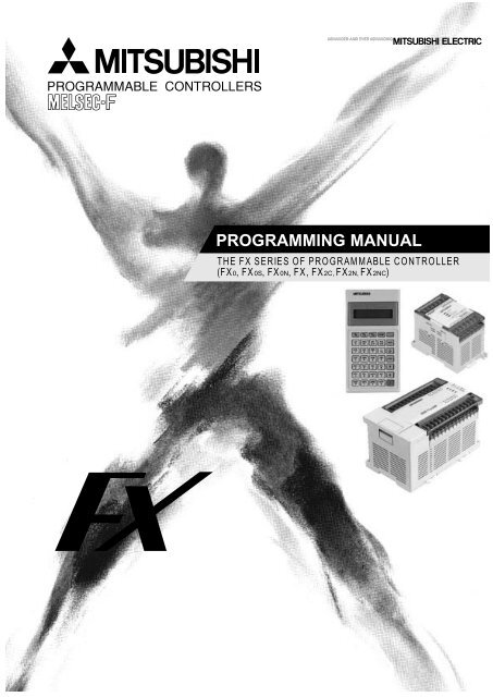
PROGRAMMING MANUALTHE <strong>FX</strong> SERIES OF PROGRAMMABLE CONTROLLER(<strong>FX</strong>0, <strong>FX</strong>0S, <strong>FX</strong>0N, <strong>FX</strong>, <strong>FX</strong>2C, <strong>FX</strong>2N, <strong>FX</strong>2NC)
<strong>FX</strong> Series Programmable Controllers<strong>FX</strong> Series Programmable Controllers<strong>Programming</strong> <strong>Manual</strong><strong>Manual</strong> number : JY992D48301<strong>Manual</strong> revision : JDate : November 1999Foreword• This manual contains text, diagrams and explanations which will guide the reader inthe correct programming and operation of the PLC.• Before attempting <strong>to</strong> install or use the PLC this manual should be read andunders<strong>to</strong>od.• If in doubt at any stage of the installation of the PLC always consult a professionalelectrical engineer who is qualified and trained <strong>to</strong> the local and national standardswhich apply <strong>to</strong> the installation site.• If in doubt about the operation or use of the PLC please consult the nearestMitsubishi Electric distribu<strong>to</strong>r.• This manual is subject <strong>to</strong> change without notice.i
<strong>FX</strong> Series Programmable ControllersFAX BACK - Combined <strong>Programming</strong> <strong>Manual</strong> (J)Mitsubishi has a world wide reputation for its efforts in continually developing and pushing backthe frontiers of industrial au<strong>to</strong>mation. What is sometimes overlooked by the user is the careand attention <strong>to</strong> detail that is taken with the documentation. However,<strong>to</strong> continue this processof improvement, the comments of the Mitsubishi users are always welcomed. This page hasbeen designed for you,the reader,<strong>to</strong> fill in your comments and fax them back <strong>to</strong> us. We look forward<strong>to</strong> hearing from you.Please tick the box of your choice;Fax numbers:Your name....................................................Mitsubishi Electric.... .....................................................................America (01) 847-478-2253 Your company ..............................................Australia (02) 638-7072 .....................................................................Germany (0 21 02) 4 86-1 12 Your location: ...............................................South Africa (0111) 444-8304 .....................................................................United Kingdom (01707) 278-695What condition did the manual arrive in? Good Minor damage UnusableWill you be using a folder <strong>to</strong> s<strong>to</strong>re the manual? Yes NoWhat do you think <strong>to</strong> the manual presentation? Tidy Un-friendlyAre the explanations understandable? Yes Not <strong>to</strong>o bad UnusableWhich explanation was most difficult <strong>to</strong> understand: ......................................................................................................................................................................................................................Are there any diagrams which are not clear? Yes NoIf so,which:..................................................................................................................................What do you think <strong>to</strong> the manual layout? Good Not <strong>to</strong>o bad Un-helpfulIf there one thing you would like <strong>to</strong> see improved,what is it?..............................................................................................................................................................................................................................................................................................................................................................Could you find the information you required easily using the index and/or the contents,if possibleplease identify your experience: ...........................................................................................................................................................................................................................................................................................................................................................................................................................................................................................................................................................................................................................................................................................................Do you have any comments in general about the Mitsubishi manuals?.....................................................................................................................................................................................................................................................................................................................................................................................................................................................................................................................................................................................................................................................Thank you for taking the time <strong>to</strong> fill out this questionnaire. We hope you found both the productand this manual easy <strong>to</strong> use.iii
<strong>FX</strong> Series Programmable Controllersiv
<strong>FX</strong> Series Programmable ControllersGuidelines for the Safety of the User and Protection of the ProgrammableController (PLC)This manual provides information for the use of the <strong>FX</strong> family of PLC’s. The manual has beenwritten <strong>to</strong> be used by trained and competent personnel. The definition of such a person orpersons is as follows;a) Any engineer who is responsible for the planning, design and construction of au<strong>to</strong>maticequipment using the product associated with this manual should be of a competentnature, trained and qualified <strong>to</strong> the local and national standards required <strong>to</strong> fulfill thatrole. These engineers should be fully aware of all aspects of safety with regards <strong>to</strong>au<strong>to</strong>mated equipment.b) Any commissioning or service engineer must be of a competent nature, trained andqualified <strong>to</strong> the local and national standards required <strong>to</strong> fulfill that job. These engineersshould also be trained in the use and maintenance of the completed product. Thisincludes being completely familiar with all associated documentation for the saidproduct. All maintenance should be carried out in accordance with established safetypractices.c) All opera<strong>to</strong>rs of the completed equipment should be trained <strong>to</strong> use that product in a safeand coordinated manner in compliance <strong>to</strong> established safety practices. The opera<strong>to</strong>rsshould also be familiar with documentation which is connected with the actual operationof the completed equipment.Note : the term ‘completed equipment’ refers <strong>to</strong> a third party constructed device whichcontains or uses the product associated with this manual.Note’s on the Symbols used in this <strong>Manual</strong>At various times through out this manual certain symbols will be used <strong>to</strong> highlight points ofinformation which are intended <strong>to</strong> ensure the users personal safety and protect the integrity ofequipment. Whenever any of the following symbols are encountered its associated note mustbe read and unders<strong>to</strong>od. Each of the symbols used will now be listed with a brief description ofits meaning.Hardware Warnings1) Indicates that the identified danger WILL cause physical and property damage.2) Indicates that the identified danger could POSSIBLY cause physical and propertydamage.3) Indicates a point of further interest or further explanation.Software Warnings4) Indicates special care must be taken when using this element of software.5) Indicates a special point which the user of the associate software element shouldbe aware of.6) Indicates a point of interest or further explanation.v
<strong>FX</strong> Series Programmable Controllersvi
<strong>FX</strong> Series Programmable Controllers3. STL <strong>Programming</strong> .................................................................................3-13.1 What is STL, SFC And IEC1131 Part 3?............................................................. 3-13.2 How STL Operates .............................................................................................. 3-23.2.1 Each step is a program ............................................................................................. 3-23.3 How To Start And End An STL Program ............................................................. 3-33.3.1 Embedded STL programs ......................................................................................... 3-33.3.2 Activating new states................................................................................................. 3-33.3.3 Terminating an STL Program .................................................................................... 3-43.4 Moving Between STL Steps ................................................................................ 3-53.4.1 Using SET <strong>to</strong> drive an STL coil ................................................................................. 3-53.4.2 Using OUT <strong>to</strong> drive an STL coil................................................................................. 3-63.5 Rules and Techniques For STL programs........................................................... 3-73.5.1 Basic Notes On The Behavior Of STL programs....................................................... 3-73.5.2 Single Signal Step Control ........................................................................................ 3-93.6 Restrictions Of Some Instructions When Used With STL.................................. 3-103.7 Using STL To Select The Most Appropriate Program ....................................... 3-113.8 Using STL To Activate Multiple Flows Simultaneously...................................... 3-123.9 General Rules For Successful STL Branching .................................................. 3-143.10 General Precautions When Using The <strong>FX</strong>-PCS/AT-EE Software ..................... 3-153.11 <strong>Programming</strong> Examples .................................................................................... 3-163.11.1 A Simple STL Flow.................................................................................................. 3-163.11.2 A Selective Branch/ First State Merge Example Program....................................... 3-183.12 Advanced STL Use............................................................................................ 3-204. Devices in Detail....................................................................................4-14.1 Inputs................................................................................................................... 4-14.2 Outputs ................................................................................................................ 4-24.3 Auxiliary Relays ................................................................................................... 4-34.3.1 General Stable State Auxiliary Relays ...................................................................... 4-34.3.2 Battery Backed/ Latched Auxiliary Relays................................................................. 4-44.3.3 Special Diagnostic Auxiliary Relays .......................................................................... 4-54.3.4 Special Single Operation Pulse Relays..................................................................... 4-54.4 State Relays ........................................................................................................ 4-64.4.1 General Stable State - State Relays ......................................................................... 4-64.4.2 Battery Backed/ Latched State Relays...................................................................... 4-74.4.3 STL Step Relays ....................................................................................................... 4-84.4.4 Annuncia<strong>to</strong>r Flags ..................................................................................................... 4-94.5 Pointers ............................................................................................................. 4-104.6 Interrupt Pointers ............................................................................................... 4-114.6.1 Input Interrupts ........................................................................................................ 4-124.6.2 Timer Interrupts ....................................................................................................... 4-124.6.3 Disabling Individual Interrupts ................................................................................. 4-134.6.4 Counter Interrupts ................................................................................................... 4-134.7 Constant K......................................................................................................... 4-144.8 Constant H......................................................................................................... 4-144.9 Timers................................................................................................................ 4-154.9.1 General timer operation........................................................................................... 4-164.9.2 Selectable Timers.................................................................................................... 4-164.9.3 Retentive Timers ..................................................................................................... 4-174.9.4 Timers Used in Interrupt and ‘CALL’ Subroutines ................................................... 4-184.9.5 Timer Accuracy ....................................................................................................... 4-184.10 Counters ............................................................................................................ 4-194.10.1 General/ Latched 16bit UP Counters ...................................................................... 4-204.10.2 General/ Latched 32bit Bi-directional Counters....................................................... 4-21ii
<strong>FX</strong> Series Programmable Controllers4.11 High Speed Counters ........................................................................................ 4-224.11.1 Basic High Speed Counter Operation ..................................................................... 4-234.11.2 Availability of High Speed Counters on <strong>FX</strong>0, <strong>FX</strong>0S and <strong>FX</strong>0N PLC’s...................... 4-244.11.3 Availability of High Speed Counters on <strong>FX</strong>, <strong>FX</strong>2C PLC’s ........................................ 4-254.11.4 Availability of High Speed Counters on <strong>FX</strong>2N(C) PLC’s .......................................... 4-284.11.5 1 Phase Counters - User Start and Reset (C235 - C240) ....................................... 4-294.11.6 1 Phase Counters - Assigned Start and Reset (C241 <strong>to</strong> C245) .............................. 4-304.11.7 2 Phase Bi-directional Counters (C246 <strong>to</strong> C250) .................................................... 4-314.11.8 A/B Phase Counters (C252 <strong>to</strong> C255) ...................................................................... 4-324.12 Data Registers................................................................................................... 4-334.12.1 General Use Registers ............................................................................................ 4-344.12.2 Battery Backed/ Latched Registers ......................................................................... 4-354.12.3 Special Diagnostic Registers................................................................................... 4-354.12.4 File Registers .......................................................................................................... 4-364.12.5Externally Adjusted Registers................................................................................... 4-374.13 Index Registers.................................................................................................. 4-384.13.1 Modifying a Constant............................................................................................... 4-394.13.2 Misuse of the Modifiers ........................................................................................... 4-394.13.3 Using Multiple Index Registers................................................................................ 4-394.14 Bits, Words, BCD and Hexadecimal.................................................................. 4-404.14.1 Bit Devices, Individual and Grouped ....................................................................... 4-404.14.2 Word Devices .......................................................................................................... 4-424.14.3 Interpreting Word Data ............................................................................................ 4-424.14.4 Two’s Compliment................................................................................................... 4-454.15 Floating Point And Scientific Notation ............................................................... 4-464.15.1 Scientific Notation.................................................................................................... 4-474.15.2 Floating Point Format .............................................................................................. 4-484.15.3 Summary Of The Scientific Notation and Floating Point Numbers.......................... 4-49iii
<strong>FX</strong> Series Programmable Controllers5.6 High Speed Processing - Functions 50 <strong>to</strong> 59 .................................................... 5-525.6.1 REF (FNC 50) ......................................................................................................... 5-535.6.2 REFF (FNC 51) ....................................................................................................... 5-535.6.3 MTR (FNC 52)......................................................................................................... 5-545.6.4 HSCS (FNC 53)....................................................................................................... 5-555.6.5 HSCR (FNC 54) ...................................................................................................... 5-565.6.6 HSZ (FNC 55) ......................................................................................................... 5-575.6.7 SPD (FNC 56) ......................................................................................................... 5-605.6.8 PLSY (FNC 57) ....................................................................................................... 5-615.6.9 PWM (FNC 58) ........................................................................................................ 5-625.6.10 PLSR (FNC 59) ....................................................................................................... 5-635.7 Handy Instructions - Functions 60 <strong>to</strong> 69 ............................................................ 5-665.7.1 IST (FNC 60) ........................................................................................................... 5-675.7.2 SER (FNC 61) ......................................................................................................... 5-695.7.3 ABSD (FNC 62) ....................................................................................................... 5-705.7.4 INCD (FNC 63) ........................................................................................................ 5-715.7.5 TTMR (FNC 64)....................................................................................................... 5-725.7.6 STMR (FNC 65) ...................................................................................................... 5-725.7.7 ALT (FNC 66) .......................................................................................................... 5-735.7.8 RAMP (FNC 67) ...................................................................................................... 5-735.7.9 ROTC (FNC 68) ...................................................................................................... 5-755.7.10 SORT (FNC 69)....................................................................................................... 5-775.8 External <strong>FX</strong> I/O Devices - Functions 70 <strong>to</strong> 79 ................................................... 5-805.8.1 TKY (FNC 70).......................................................................................................... 5-815.8.2 HKY (FNC 71) ......................................................................................................... 5-825.8.3 DSW (FNC 72) ........................................................................................................ 5-835.8.4 SEGD (FNC 73) ...................................................................................................... 5-845.8.5 SEGL (FNC 74) ....................................................................................................... 5-855.8.6 ARWS (FNC 75) ...................................................................................................... 5-875.8.7 ASC (FNC 76) ......................................................................................................... 5-885.8.8 PR (FNC 77)............................................................................................................ 5-895.8.9 FROM (FNC 78) ...................................................................................................... 5-905.8.10 TO (FNC 77)............................................................................................................ 5-915.9 External <strong>FX</strong> Serial Devices - Functions 80 <strong>to</strong> 89 ............................................... 5-945.9.1 RS (FNC 80)............................................................................................................ 5-965.9.2 RUN (FNC 81)......................................................................................................... 5-975.9.3 ASCI (FNC 82) ........................................................................................................ 5-995.9.4 HEX (FNC 83) ....................................................................................................... 5-1005.9.5 CCD (FNC 84)....................................................................................................... 5-1015.9.6 VRRD (FNC 85) .................................................................................................... 5-1025.9.7 VRSD (FNC 86)..................................................................................................... 5-1025.9.8 PID (FNC 88)......................................................................................................... 5-1035.10 External F2 Units - Functions 90 <strong>to</strong> 99 ............................................................ 5-1115.10.1 MNET (FNC 90) .................................................................................................... 5-1125.10.2 ANRD (FNC 91) .................................................................................................... 5-1125.10.3 ANWR (FNC 92).................................................................................................... 5-1135.10.4 RMST (FNC 93) .................................................................................................... 5-1135.10.5 RMMR (FNC 94) ................................................................................................... 5-1145.10.6 RMRD (FNC 95) .................................................................................................... 5-1155.10.7 RMMN (FNC 96) ................................................................................................... 5-1155.10.8 BLK (FNC 97)........................................................................................................ 5-1165.10.9 MCDE (FNC 98) .................................................................................................... 5-117v
<strong>FX</strong> Series Programmable Controllers5.11 Floating Point 1 & 2 - Functions 110 <strong>to</strong> 129 .................................................... 5-1195.11.1 ECMP (FNC 110) .................................................................................................. 5-1215.11.2 EZCP (FNC 111) ................................................................................................... 5-1215.11.3 EBCD (FNC 118)................................................................................................... 5-1225.11.4 EBIN (FNC 119) .................................................................................................... 5-1225.11.5 EADD (FNC 120)................................................................................................... 5-1235.11.6 EAUB (FNC 121) ................................................................................................... 5-1245.11.7 EMUL (FNC 122)................................................................................................... 5-1245.11.8 EDIV (FNC 123) .................................................................................................... 5-1255.11.9 ESQR (FNC 127) .................................................................................................. 5-1255.11.10INT (FNC 129) ...................................................................................................... 5-1265.12 Trigonometry - FNC 130 <strong>to</strong> FNC 139 .............................................................. 5-1285.12.1 SIN (FNC 130)....................................................................................................... 5-1295.12.2 COS (FNC 131) ..................................................................................................... 5-1305.12.3 TAN (FNC 132) ..................................................................................................... 5-1305.13 Data Operations 2 - FNC 140 <strong>to</strong> FNC 149 ...................................................... 5-1325.13.1 SWAP (FNC 147) .................................................................................................. 5-1335.14 Real Time Clock Control - FNC 160 <strong>to</strong> FNC 169............................................. 5-1365.14.1 TCMP (FNC 160) .................................................................................................. 5-1375.14.2 TZCP (FNC 161) ................................................................................................... 5-1385.14.3 TADD (FNC 162) ................................................................................................... 5-1395.14.4 TSUB (FNC 163) ................................................................................................... 5-1405.14.5 TRD (FNC 166) ..................................................................................................... 5-1415.14.6 TWR (FNC 167) .................................................................................................... 5-1425.15 Gray Codes - FNC 170 <strong>to</strong> FNC 179 ................................................................ 5-1445.15.1 GRY (FNC 170) ..................................................................................................... 5-1455.15.2 GBIN (FNC 171) .................................................................................................... 5-1455.16 Inline Comparisons - FNC 220 <strong>to</strong> FNC 249..................................................... 5-1485.16.1 LD compare (FNC 224 <strong>to</strong> 230) .............................................................................. 5-1495.16.2 AND compare (FNC 232 <strong>to</strong> 238) ........................................................................... 5-1505.16.3 OR compare (FNC 240 <strong>to</strong> 246) ............................................................................. 5-1516. Diagnostic Devices................................................................................6-16.1 PLC Status (M8000 <strong>to</strong> M8009 and D8000 <strong>to</strong> D8009).......................................... 6-26.2 Clock Devices (M8010 <strong>to</strong> M8019 and D8010 <strong>to</strong> D8019) ................................... 6-36.3 Operation Flags ................................................................................................... 6-46.4 PLC Operation Mode (M8030 <strong>to</strong> M8039 and D8030 <strong>to</strong> D8039) ......................... 6-56.5 Step Ladder (STL) Flags (M8040 <strong>to</strong> M8049 and D8040 <strong>to</strong> D8049) ................... 6-66.6 Interrupt Control Flags (M8050 <strong>to</strong> M8059 and D8050 <strong>to</strong> D8059) ...................... 6-76.7 Error Detection Devices (M8060 <strong>to</strong> M8069 and D8060 <strong>to</strong> D6069) ..................... 6-86.8 Link And Special Operation Devices (M8070 <strong>to</strong> M8099 and D8070 <strong>to</strong> D8099) .. 6-96.9 Miscellaneous Devices (M8100 <strong>to</strong> M8119 and D8100 <strong>to</strong> D8119) ..................... 6-106.10 Communication Adapter Devices, i.e. 232ADP, 485ADP ................................ 6-106.11 High Speed Zone Compare Table Comparison Flags ..................................... 6-116.12 Miscellaneous Devices (M8160 <strong>to</strong> M8199) ....................................................... 6-126.13 Index Registers (D8180 <strong>to</strong> D8199) ................................................................... 6-136.14 Up/Down Counter Control (M8200 <strong>to</strong> M8234 and M8200 <strong>to</strong> D8234) ............... 6-146.15 High Speed Counter Control (M8235 <strong>to</strong> M8255 and D8235 <strong>to</strong> D8255) ............ 6-146.16 Error Code Tables ............................................................................................. 6-15vi
<strong>FX</strong> Series Programmable Controllers7. Execution Times And Instructional Hierarchy........................................7-17.1 Basic Instructions ................................................................................................ 7-17.2 Applied Instructions ............................................................................................ 7-37.3 Hierarchical Relationships Of Basic Program Instructions ................................ 7-127.4 Batch Processing............................................................................................... 7-147.5 Summary of Device Memory Allocations........................................................... 7-147.6 Limits Of Instruction Usage ............................................................................... 7-167.6.1 Instructions Which Can Only Be Used Once In The Main Program Area ............... 7-167.6.2 Instructions Which Are Not Suitable For Use With 110V AC Input Units ................ 7-168. PLC Device Tables................................................................................8-18.1 Performance Specification Of The <strong>FX</strong>0 And <strong>FX</strong>0S ............................................. 8-18.2 Performance Specification Of The <strong>FX</strong>0N ............................................................ 8-28.3 Performance Specification Of The <strong>FX</strong> (CPU versions 2.0 <strong>to</strong> 3.06) ..................... 8-48.4 Performance Specification Of The <strong>FX</strong>(CPU versions from 3.07) And <strong>FX</strong>2C (all versions) ......................................8-68.5 Performance Specification Of The <strong>FX</strong>2N(C) ....................................................... 8-89. Assigning System Devices ....................................................................9-19.1 Addressing Extension Modules ........................................................................... 9-19.2 Using The <strong>FX</strong>2-24EI With F Series Special Function Blocks .............................. 9-29.2.1 Using the <strong>FX</strong>2-24EI With A F-16NP/NT .................................................................... 9-39.2.2 Using the <strong>FX</strong>2-24EI With A F2-6A............................................................................. 9-49.2.3 Using the <strong>FX</strong>2-24EI With A F2-32RM ....................................................................... 9-49.2.4 Using the <strong>FX</strong>2-24EI With A F2-30GM ....................................................................... 9-59.3 Parallel Link Adapters.......................................................................................... 9-69.4 Real Time Clock Function ................................................................................... 9-79.4.1 Setting the real time clock ......................................................................................... 9-810.Points Of Technique...........................................................................10-110.1 Advanced <strong>Programming</strong> Points ......................................................................... 10-110.2 Users of DC Powered <strong>FX</strong> Units ......................................................................... 10-110.3 Using The Forced RUN/STOP Flags................................................................. 10-210.3.1 A RUN/STOP push but<strong>to</strong>n configuration ................................................................. 10-210.3.2 Remote RUN/STOP control .................................................................................... 10-310.4 Constant Scan Mode ......................................................................................... 10-410.5 Alternating ON/OFF States................................................................................ 10-410.6 Using Battery Backed Devices For Maximum Advantage ................................. 10-510.7 Indexing Through Multiple Display Data Values................................................ 10-510.8 Reading And Manipulating Thumbwheel Data .................................................. 10-610.9 Measuring a High Speed Pulse Input ................................................................ 10-610.9.1 A 1 msec timer pulse measurement........................................................................ 10-610.9.2 A 0.1 msec timer pulse measurement..................................................................... 10-710.10Using The Execution Complete Flag, M8029 ................................................... 10-710.11Creating a User Defined MTR Instruction ......................................................... 10-810.12An Example System Application Using STL And IST Program Control............ 10-810.13Using The PWM Instruction For Mo<strong>to</strong>r Control ............................................... 10-1510.14Communication Format................................................................................... 10-1810.14.1Specification of the communication parameters: .................................................. 10-1810.14.2Header and Termina<strong>to</strong>r Characters ...................................................................... 10-1910.14.3Timing diagrams for communications: .................................................................. 10-2010.14.48 bit or 16 bit communications.............................................................................. 10-23vii
<strong>FX</strong> Series Programmable Controllers10.15PID <strong>Programming</strong> Techniques........................................................................ 10-2410.15.1Keeping MV within a set range............................................................................. 10-2410.15.2<strong>Manual</strong>/Au<strong>to</strong>matic change over ............................................................................ 10-2410.15.3Using the PID alarm signals ................................................................................. 10-2510.15.4Other tips for PID programming............................................................................ 10-2510.16Additional PID functions.................................................................................. 10-2610.16.1Output Value range control (S3+1 b5).................................................................. 10-2610.17Pre-tuning operation ....................................................................................... 10-2710.17.1Variable Constants ............................................................................................... 10-2710.18Example Au<strong>to</strong>tuning Program ......................................................................... 10-2811.Index...................................................................................................11-111.1 Index.................................................................................................................. 11-111.2 ASCII Character Codes ..................................................................................... 11-911.3 Applied Instruction List .................................................................................... 11-10viii
<strong>FX</strong> Series Programmable Controllers Introduction 11 Introduction2 Basic Program Instructions3 STL <strong>Programming</strong>4 Devices in Detail5 Applied Instructions6 Diagnostic Devices7 Instruction Execution Times8 PLC Device Tables9 Assigning System Devices10 Points of Technique11 Index
<strong>FX</strong> Series Programmable Controllers Introduction 1Chapter Contents1. Introduction............................................................................................1-11.1 Overview.............................................................................................................. 1-11.2 What is a ProgrammableController? ................................................................... 1-21.3 What do You Need <strong>to</strong> Program a PC? ................................................................ 1-21.4 CPU version numbers ......................................................................................... 1-31.4.1 <strong>FX</strong>0N CPU versions................................................................................................... 1-31.4.2 <strong>FX</strong> and <strong>FX</strong>2C CPU versions....................................................................................... 1-31.5 Special considerations for programming equipment ........................................... 1-41.5.1 <strong>FX</strong> CPU version 3.07 or later and <strong>FX</strong>2C ................................................................... 1-41.5.2 <strong>FX</strong>2N CPU all versions ............................................................................................. 1-5
Introduction 11. Introduction<strong>FX</strong>0(S) <strong>FX</strong>0N <strong>FX</strong> <strong>FX</strong>(2C) <strong>FX</strong>2N(C)1.1 Overview1) Scope of this manualThis manual gives details on all aspects of operation and programming for <strong>FX</strong>, <strong>FX</strong>2C, <strong>FX</strong>0N,<strong>FX</strong>0S, <strong>FX</strong>0, <strong>FX</strong>2N and <strong>FX</strong>2NC programmable controllers (PLCs). For all information relating <strong>to</strong>the PLC hardware and installation, refer <strong>to</strong> the appropriate manual supplied with the unit.2) How <strong>to</strong> use this manualThis manual covers all the functions of the highest specification Programmable (Logic)Controller (PLC). For this reason, the following indica<strong>to</strong>r is included in relevant section titles<strong>to</strong> show which PLCs that section applies <strong>to</strong>;Shaded boxes indicate<strong>FX</strong>0(S) <strong>FX</strong>0N <strong>FX</strong> <strong>FX</strong>(2C) <strong>FX</strong>2N(C)the applicable PLC type- “<strong>FX</strong>0(S)” - All <strong>FX</strong>0 and <strong>FX</strong>0S PLCs- “<strong>FX</strong>0N” - All <strong>FX</strong>0N PLCs- “<strong>FX</strong>” - All <strong>FX</strong> and <strong>FX</strong>2 PLCs (CPU ver 2.30 or earlier)- “<strong>FX</strong>(2C)” - All <strong>FX</strong> and <strong>FX</strong>2 PLCs (CPU versions 3.07 or later)- - All <strong>FX</strong>2C PLCs (see page 1-4)- “<strong>FX</strong>2N(C)” - All <strong>FX</strong>2N and <strong>FX</strong>2NC PLCs<strong>FX</strong>0(S) <strong>FX</strong>0N <strong>FX</strong> <strong>FX</strong>(2C) <strong>FX</strong>2N(C)If an indica<strong>to</strong>r box is half shaded, as shown <strong>to</strong> theleft, this means that not all the functions described inthe current section apply <strong>to</strong> that PLC. The textexplains in further detail or makes an independentreference.If there are no indica<strong>to</strong>r boxes then assume the section applies <strong>to</strong> all PLC types unlessotherwise stated.3) <strong>FX</strong> familyThis is a generic term which is often used <strong>to</strong> describe all Programmable Controllers withoutidentifying individual types or model names.4) CPU version numbers and programming supportAs Mitsubishi upgrades each model different versions have different capabilities.- Please refer <strong>to</strong> section 1.4 for details about version numbers and capabilities.- Please refer <strong>to</strong> section 1.5 for details about peripheral support for each model.1-1
Introduction 11.2 What is a Programmable Controller?<strong>FX</strong>0(S) <strong>FX</strong>0N <strong>FX</strong> <strong>FX</strong>(2C) <strong>FX</strong>2N(C)A Programmable Logic Controller (PLC or programmable controller) is a device that a user canprogram <strong>to</strong> perform a series or sequence of events. These events are triggered by stimuli(usually called inputs) received at the PLC or through delayed actions such as time delays orcounted occur-rences. Once an event triggers, it actuates in the outside world by switching ONor OFF electronic control gear or the physical actuation of devices. A programmable controllerwill continually ‘loop’ through its internal ‘user defined’ program waiting for inputs and givingoutputs at the programmed specific times.Note on terminology:The term programmable controller is a generic word used <strong>to</strong> bring all the elements making thecontrol system under one descriptive name. Sometimes engineers use the term‘Programmable Logic Controller’, ‘PLC’ or ‘programmable controller’ <strong>to</strong> describe the samecontrol system.The construction of a programmable controller can be broken down in<strong>to</strong> component parts. Theelement where the program is loaded, s<strong>to</strong>red and processed is often known as the MainProcessing Unit or MPU. Other terms commonly heard <strong>to</strong> describe this device are ‘base unit’,‘controller’ and ‘CPU’. The term CPU is a little misleading as <strong>to</strong>days more advanced productsmay contain local CPU devices. A Main CPU (or more correctly a Main Processing Unit)controls these local CPUs through a communication network or bus.1.3 What do You Need <strong>to</strong> Program a PLC?<strong>FX</strong>0(S) <strong>FX</strong>0N <strong>FX</strong> <strong>FX</strong>(2C) <strong>FX</strong>2N(C)A variety of <strong>to</strong>ols are available <strong>to</strong> program the Mitsubishi <strong>FX</strong> family of PLCs. Each of these<strong>to</strong>ols can use and access the instructions and devices listed in this manual for the identifiedPLC.A6GPP<strong>FX</strong>-A6GPP-EE-KIT<strong>FX</strong>,<strong>FX</strong>2CPersonal computerMelsec MEDOCMelsec Medoc PlusSW1PC-<strong>FX</strong>GPEE<strong>FX</strong>-PCS-WIN-EGP80GP-80<strong>FX</strong>-E-KIT<strong>FX</strong>2N(C)Op<strong>to</strong>-isolatedRS232/RS422interfaceHPP<strong>FX</strong>-10P-E<strong>FX</strong>-20P-E<strong>FX</strong>0, <strong>FX</strong>0S,<strong>FX</strong>0N1-2
Introduction 11.4 CPU version numbers<strong>FX</strong>0(S) <strong>FX</strong>0N <strong>FX</strong> <strong>FX</strong>(2C) <strong>FX</strong>2N(C)Over time Mitsubishi adds newer and better features <strong>to</strong> develop and enhance the products.Because of the nature of PLCs, that can be likened <strong>to</strong> ‘industrial computers’, changessometimes occur within the units main CPU (Central Processing Unit). These changes aresimilar <strong>to</strong> those experienced by office and home computer users, that is, going <strong>to</strong> a version upprocessor. The following lists identify the CPU versions that had significant upgrades or newfunctions and features added.1.4.1 <strong>FX</strong>0N CPU versionsCPU Ver 1.20CPU Ver 1.401.4.2 <strong>FX</strong> and <strong>FX</strong>2C CPU versionsCPU Ver 3.07CPU Ver 3.11CPU Ver 3.2CPU Ver 3.30The following features were added:Software control for pro<strong>to</strong>col 1 and 4 communications with the <strong>FX</strong>0N-485ADP,1:N network.The following features were added:Software control for communications using the <strong>FX</strong>0N-485ADP, peer <strong>to</strong> peer(N:N) network.The following instructions were added:ASCI (FNC82), CCD (FNC84), FLT (FNC49), HEX (FNC83), RS (FNC80),SER (FNC61), SORT (FNC69), SQR (FNC48)The following instructions were upgraded:EI (FNC04), BMOV (FNC15), HSCS (FNC53), PLSY (FNC57),FMOV (FNC16), MEAN (FNC45), ABSD (FNC62), DSW (FNC72),SEGL (74),PR (FNC 77)The following device ranges were added:Input and output devices are independently addressable up<strong>to</strong> 256 points insoftware. Total combined input and output points (hardware or software) is256.Auxiliary relays increased <strong>to</strong> 1536 points (M0-M1535)Data registers increased <strong>to</strong> 1000 points (D0-D999)Optional RAM File Registers added, 2000 points (D6000 -D7999)Pointers increased <strong>to</strong> 128 points (P0 - P127)The following instructions were added:PID (FNC88)The following features were added:Software control for pro<strong>to</strong>col 4 communications with the <strong>FX</strong>-485ADP, 1:Nnetwork.The following features were added:Software control for pro<strong>to</strong>col 1 communications with the <strong>FX</strong>-485ADP, 1:Nnetwork.The following instructions were phased out (removed):ANRD (FNC91), ANWR (FNC92), BLK (FNC97), MCDE (FNC98), MNET(FNC90)1-3
Introduction 11.5 Special considerations for programming equipment1.5.1 <strong>FX</strong> CPU version 3.07 or later and <strong>FX</strong>2CPeripherals TableSystem software version which will.......Description Model Number ....require the use ofauxiliary M coils....program all instructionsdirectlyHand heldprogrammer (HHP)<strong>FX</strong>-10P-E V 1.10 from V 2.00HHP cassette <strong>FX</strong>-20P-M<strong>FX</strong>A-E V 1.20 from V 2.00<strong>Programming</strong> <strong>FX</strong>-PCS/AT-E-KIT V 1.01 from V 2.00software <strong>FX</strong>-A6GPP-E-KIT V 1.00 from V 2.00Data access units<strong>FX</strong>0(S) <strong>FX</strong>0N <strong>FX</strong> <strong>FX</strong>(2C) <strong>FX</strong>2N(C)<strong>Programming</strong> <strong>to</strong>ols operating old system software can not access the new features added <strong>to</strong>the <strong>FX</strong> CPU from version 3.07 (and available on all <strong>FX</strong>2C units). However, programmingcertain ‘standard’ applied instructions in conjunction with special auxiliary coils (M coils) canachieve the same ’effective instruction’ as the new instructions. The following tables identifywhich version of peripheral software will work directly with all of the ’new’ features and whichperipheral software versions require use of modified instructions.<strong>FX</strong>-10DU-E V 1.10 from V 2.00<strong>FX</strong>-20DU-E V 1.10 from V 2.00Other DU units from V 1.00Existing Instruction And Special M Coil Combination To Mimic The Operation Of TheIdentified InstructionExisting <strong>FX</strong> instruction used <strong>to</strong> mimic the operation of......Mnemonic FNC number Modifying M coil Mimicked instruction Mnemonic FNC NumberMOV 12 M8190 Square root SQR 48MOV 12 M8191 Float FLT 49RAMP 67 M8193 Data search SER 61RAMP 67 M8194 RS232 instruction RS 80FMOV 16 M8196 Hex <strong>to</strong> ASCII conversion ASCI 82FMOV 16 M8197 ASCII <strong>to</strong> Hex conversion HEX 83FMOV 16 M8195 Sum check CCD 84 Example usageThis format is very important for the instruction <strong>to</strong> operatecorrectly.The user must program the ’mimic’ instructionwith the modifying M coil in a SET instruction immediatelybefore the instruction <strong>to</strong> be modified. 1-4
Introduction 1Using the new Interrupt Pointers:To program new Interrupt Pointers I010through I060 in <strong>to</strong> the HSCS (FNC 53)instruction with older programmingequipment, substitute the followingspecial M codes for the appropriateInterrupt Pointer; see the table right.Existing Instruction And Special M CoilCombination To Mimic The OperationOf The Identified Interrupt pointerExisting Auxiliary Coilused <strong>to</strong> replace the identifiedInterrupt PointerInterrupt PointerM8181I010M8182I020M8183I030M8184I040M8185I050M8186I060Using M8198 with the BMOV instruction:With old software and peripherals, file registers can not be used as a destination device in theBMOV (FNC 15) instruction. To BMOV data in<strong>to</strong> file registers with old equipment set special Mcoil M8198 on. This switches the source and destination parameters; i.e., the source is thentreated as the destination and the destination becomes the source.General note:Ignore the special programming techniques identified in this section if using updatedprogramming software or peripherals; then normal operation, as identifiedin the followingsections, will apply.1.5.2 <strong>FX</strong>2N(C) CPU all versions<strong>FX</strong>0(S) <strong>FX</strong>0N <strong>FX</strong> <strong>FX</strong>(2C) <strong>FX</strong>2N(C)The introduction of this CPU provides the <strong>FX</strong> user with many new devices and instructions. Touse the full features of the <strong>FX</strong>2N(C) units the user must upgrade older software and hardwareprogramming <strong>to</strong>ols.However, because of the downward compatibility of the <strong>FX</strong>2N(C), it is not necessary <strong>to</strong> upgradeexisting programming <strong>to</strong>ols for use with <strong>FX</strong>2N(C) units up <strong>to</strong> the equivalent functionality of <strong>FX</strong>CPU ver 3.30 units.Peripherals TableDescriptionModel NumberSystem software version withfull support for <strong>FX</strong>2N(c)Hand held programmer (HHP) <strong>FX</strong>-10P-E from V 3.00HHP cassette <strong>FX</strong>-20P-M<strong>FX</strong>A-E from V 3.00Data access units<strong>FX</strong>-10DU-E from V 4.00<strong>FX</strong>-20DU-ESupports up <strong>to</strong> <strong>FX</strong> devices only<strong>FX</strong>-25DU-E from V 2.00<strong>FX</strong>-30DU-E from V 3.00<strong>FX</strong>-40DU-E(S)Supports up <strong>to</strong> <strong>FX</strong> devices only<strong>FX</strong>-40DU-TK-ES from V 3.00<strong>FX</strong>-50DU-TK(S)-E from V 2.10F940GOT-SWD(LWD)-E All versions1-5
Introduction 1MEMO1-6
<strong>FX</strong> Series Programmable Controllers Basic Program Instructions 21 Introduction2 Basic Program Instructions3 STL <strong>Programming</strong>4 Devices in Detail5 Applied Instructions6 Diagnostic Devices7 Instruction Execution Times8 PLC Device Tables9 Assigning System Devices10 Points of Technique11 Index
<strong>FX</strong> Series Programmable Controllers Basic Program Instructions 2Chapter Contents2. Basic Program Instructions ...................................................................2-12.1 What is a Program?............................................................................................. 2-12.2 Outline of Basic Devices Used in <strong>Programming</strong>.................................................. 2-12.3 How <strong>to</strong> Read Ladder Logic .................................................................................. 2-22.4 Load, Load Inverse.............................................................................................. 2-32.5 Out....................................................................................................................... 2-42.5.1 Timer and Counter Variations ................................................................................... 2-42.5.2 Double Coil Designation............................................................................................ 2-52.6 And, And Inverse ................................................................................................. 2-62.7 Or, Or Inverse...................................................................................................... 2-72.8 Load Pulse, Load Trailing Pulse.......................................................................... 2-82.9 And Pulse, And Trailing Pulse ............................................................................. 2-92.10 Or Pulse, Or Trailing Pulse................................................................................ 2-102.11 Or Block............................................................................................................. 2-112.12 And Block .......................................................................................................... 2-122.13 MPS, MRD and MPP......................................................................................... 2-132.14 Master Control and Reset.................................................................................. 2-152.15 Set and Reset.................................................................................................... 2-172.16 Timer, Counter(Out & Reset)............................................................................. 2-182.16.1 Basic Timers, Retentive Timers And Counters........................................................ 2-182.16.2 Normal 32 bit Counters ........................................................................................... 2-192.16.3 High Speed Counters .............................................................................................. 2-192.17 Leading and Trailing Pulse ................................................................................ 2-202.18 Inverse............................................................................................................... 2-212.19 No Operation ..................................................................................................... 2-222.20 End .................................................................................................................... 2-23
<strong>FX</strong> Series Programmable ControllersBasic Program Instructions 22. Basic Program Instructions2.1 What is a Program?A program is a connected series of instructions written in a language that the PLC canunderstand. There are three forms of program format; instruction, ladder and SFC/STL. Not allprogramming <strong>to</strong>ols can work in all programming forms. Generally hand held programmingpanels only work with instruction format while most graphic programming <strong>to</strong>ols will work withboth instruction and ladder format. Specialist programming software will also allow SFC styleprogramming.LDOUTANDSETLDOUTX10Y7M38S5X21T01K40Instruction format Ladder Format SFC Format2.2 Outline of Basic Devices Used in <strong>Programming</strong>There are six basic programming devices. Each device has its own unique use. To enablequick and easy identification each device is assigned a single reference letter;- X: This is used <strong>to</strong> identify all direct, physical inputs <strong>to</strong> the PLC.- Y: This is used <strong>to</strong> identify all direct, physical outputs from the PLC.- T: This is used <strong>to</strong> identify a timing device which is contained within the PLC.- C: This is used <strong>to</strong> identify a counting device which is contained within the PLC.- M and S: These are used as internal operation flags within the PLC.All of the devices mentioned above are known as ‘bit devices’. This is a descriptive title tellingthe user that these devices only have two states; ON or OFF, 1 or 0.Detailed device information:• Chapter 4 contains this information in detail. However, the above is all that isrequired for the rest of this chapter.2-1
<strong>FX</strong> Series Programmable Controllers Basic Program Instructions 22.3 How <strong>to</strong> Read Ladder LogicLadder logic is very closely associated <strong>to</strong> basic relay logic. There are both contacts and coilsthat can be loaded and driven in different configurations. However, the basic principle remainsthe same.A coil drives direct outputs of the PLC (ex. a Y device) or drives internal timers, counters orflags (ex. T, C, M and S devices). Each coil has associated contacts. These contacts areavailable in both “normally open” (NO) and “normally closed” (NC) configurations.The term “normal(ly)” refers <strong>to</strong> the status of the contacts when the coil is not energized. Usinga relay analogy, when the coil is OFF, a NO contact would have no current flow, that is, a loadbeing supplied through a NO contact would not operate. However, a NC contact would allowcurrent <strong>to</strong> flow, hence the connected load would be active.Activating the coil reverses the contact status, that is, the current would flow in a NO contactand a NC contact would inhibit the flow.Physical inputs <strong>to</strong> the PLC (X devices) have no programmable coil. These devices may only beused in a contact format (NO and NC types are available).Example:Because of the close relay association, ladder logic programs can be read as current flowingfrom the left vertical line <strong>to</strong> the right vertical line. This current must pass through a series ofcontact representations such as X0 and X1 in order <strong>to</strong> switch the output coil Y0 ON. Therefore,in the example shown, switching X0 ON causes the output Y0 <strong>to</strong> also switch ON. If however,the limit switch X1 is activates, the output Y0 turns OFF. This is because the connectionbetween the left and the right vertical lines breaks so there is no current flow.Mo<strong>to</strong>rToggle switchLimit switchX0X1INPUTProgrammable ControllerPC ProgramX0 X1Y0DC Power SupplyOUTPUTY0COM(Y0)ACPowerSupply2-2
<strong>FX</strong> Series Programmable Controllers Basic Program Instructions 22.4 Load, Load Inverse<strong>FX</strong>0(S) <strong>FX</strong>0N <strong>FX</strong> <strong>FX</strong>(2C) <strong>FX</strong>2N(C)Mnemonic Function Format Devices Program stepsLD(LoaD)Initial logicaloperation contacttype NO(normally open)X, Y, M, S, T, C 1LDI(LoaD Inverse)Initial logicaloperation contacttype NC(normally closed)X, Y, M, S, T, C 1Program example:X0X1T0LDIKY0M100T0K19Y10123478LDOUTLDIOUTOUTSPLDOUTXYXMTKTY00110001901When using hand heldprogrammers, the space keyneeds <strong>to</strong> be pressed <strong>to</strong> enablethe constant <strong>to</strong> be entered.Basic points <strong>to</strong> remember:- Connect the LD and LDI instructions directly <strong>to</strong> the left hand bus bar.- Or use LD and LDI instructions <strong>to</strong> define a new block of program when using the ORBand ANB instructions (see later sections).The OUT instruction:• For details of the OUT instruction (including basic timer and counter variations)please see over the following page.2-3
<strong>FX</strong> Series Programmable Controllers Basic Program Instructions 22.5 Out<strong>FX</strong>0(S) <strong>FX</strong>0N <strong>FX</strong> <strong>FX</strong>(2C) <strong>FX</strong>2N(C)Mnemonic Function Format Devices Program stepsOUT(OUT)Final logicaloperation type coildriveY, M, S, T, CY, M:1S, special Mcoils: 2T:3C (16 bit): 3C (32 bit): 5Basic points <strong>to</strong> remember:- Connect the OUT instruction directly <strong>to</strong> the right hand bus bar.- It is not possible <strong>to</strong> use the OUT instruction <strong>to</strong> drive ‘X’ type input devices.- It is possible <strong>to</strong> connect multiple OUT instructions in parallel (for example see theprevious page; M100/T0 configuration)2.5.1 Timer and Counter VariationsWhen configuring the OUT instruction for use as either a timer (T) or counter (C) a constantmust also be entered. The constant is identified by the letter “K” (for example see previouspage; T0 K19).In the case of a timer, the constant “K” holds the duration data for the timer <strong>to</strong> operate, i.e. if a100 msec timer has a constant of “K100” it will be (1005 100 msec) 10 seconds before thetimer coil activates.With counters, the constant identifies how many times the counter must be pulsed or triggeredbefore the counter coil activates. For example, a counter with a constant of “8” must betriggered 8 times before the counter coil finally energizes.The following table identifies some basic parameter data for various timers and counters;Timer/Counter Setting constant K Actual setting Program steps1 msec Timer0.001 <strong>to</strong> 32.767 sec10 msec Timer 1 <strong>to</strong> 32,7670.01 <strong>to</strong> 327.67 sec100 msec Timer 0.1 <strong>to</strong> 3276.7 sec316 bit Counter 1 <strong>to</strong> 32,767 1 <strong>to</strong> 32,76732 bit Counter-2,147,483,648 <strong>to</strong>2,147,483,647-2,147,483,648 <strong>to</strong>2,147,483,64752-4
<strong>FX</strong> Series Programmable Controllers Basic Program Instructions 22.5.2 Double Coil DesignationDouble or dual coiling is not a recommended1.practice. Using multiple output coils of thesame device can cause the prog ramX1operation <strong>to</strong> become unreliable. The exampleY3program shown opposite identifies a doublecoil situation; there are two Y3 outputs. TheY3following sequence of events will occur whenY4 inputs X1 = ON and X2 = OFF;2.1.The first Y3 tuns ON because X1 is ON. TheX2contacts associated with Y3 also energizeY3 when the coil of output Y3 energizes. Hence,output Y4 turns ON.2.The last and most important line in thisprogram looks at the status of input X2.If this is NOT ON then the second Y3 coil does NOT activate. Therefore the status of the Y3coil updates <strong>to</strong> reflect this new situation, i.e. it turns OFF. The final outputs are then Y3 = OFFand Y4 = ON.Use of dual coils:• Always check programs for incidents of dual coiling. If there are dual coils theprogram will not operate as expected - possibly resulting in unforeseen physicalThe last coil effect:• In a dual coil designation, the coil operation designated last is the effective coil. Thatis, it is the status of the previous coil that dictates the behavior at the current point inthe program.1 t secs2 3564 4: Input ON state NOT recognized: Input ON state recognized: Input OFF state NOT recognized: 1 program processing: Input processing: Output processing: A full program scan/operation cycle7Input durations:The ON or OFF duration of the PLC inputsmust be longer than the operation cycletime of the PLC.Taking a 10 msec (standard input filter)response delay in<strong>to</strong> account, the ON/OFFduration must be longer than 20 msec ifthe operation cycle (scan time) is 10 msec.Therefore, in this example, input pulses ofmore than 25Hz (1sec/(20msec ON +20msec OFF)) cannot be sensed.There are applied instructions provided <strong>to</strong>handle such high speed input requests.2-5
<strong>FX</strong> Series Programmable Controllers Basic Program Instructions 22.6 And, And Inverse<strong>FX</strong>0(S) <strong>FX</strong>0N <strong>FX</strong> <strong>FX</strong>(2C) <strong>FX</strong>2N(C)Mnemonic Function Format Devices Program stepsAND(AND)Serial connectionof NO (normallyopen) contactsX, Y, M, S, T, C 1ANI(AND Inverse)Serial connectionof NC (normallyclosed) contactsX, Y, M, S, T, C 1Program example:ANDX2Y3ANIX0X3T1Y3M101Y401234567LDANDOUTLDANIOUTANDOUTXXYYXMTY2033310114ANDBasic points <strong>to</strong> remember:- Use the AND and ANI instructions for serial connection of contacts. As many contacts asrequired can be connected in series (see following point headed “Peripheral limitations”).- The output processing <strong>to</strong> a coil, through a contact, after writing the initial OUT instructionis called a “follow-on” output (for an example see the program above; OUT Y4). Followonoutputs are permitted repeatedly as long as the output order is correct.Peripheral limitations:• The PLC has no limit <strong>to</strong> the number of contacts connected in series or in parallel.However, some programming panels, screens and printers will not be able <strong>to</strong> displayor print the program if it exceeds the limit of the hardware. It is preferable for eachline or rung of ladder program <strong>to</strong> contain up <strong>to</strong> a maximum of 10 contacts and 1 coil.Also, keep the number of follow-on outputs <strong>to</strong> a maximum of 24.2-6
<strong>FX</strong> Series Programmable Controllers Basic Program Instructions 22.7 Or, Or Inverse<strong>FX</strong>0(S) <strong>FX</strong>0N <strong>FX</strong> <strong>FX</strong>(2C) <strong>FX</strong>2N(C)Mnemonic Function Format Devices Program stepsOR(OR)ORI(OR Inverse)Parallelconnection of NO(normally open)contactsParallelconnection of NC(normally closed)contactsX, Y, M, S, T, C 1X, Y, M, S, T, C 1Program example:X4X6ORM102ORIY5 X7 X10M103Y5M1030123456789LDORORIOUTLDIANDORANIOROUTXXMYYXMXMM4610255710310110103M110Basic points <strong>to</strong> remember:- Use the OR and ORI instructions for parallel connection of contacts. To connect a blockthat contains more than one contact connected in series <strong>to</strong> another circuit block inparallel, use an ORB instruction.- Connect one side of the OR/ORI instruction <strong>to</strong> the left hand bus bar.Peripheral limitations:• The PLC has no limit <strong>to</strong> the number of contacts connected in series or in parallel.However, some programming panels, screens and printers will not be able <strong>to</strong> displayor print the program if it exceeds the limit of the hardware. It is preferable for eachline or rung of ladder program <strong>to</strong> contain up <strong>to</strong> a maximum of 10 contacts and 1 coil.Also keep number of follow-on outputs <strong>to</strong> a maximum of 24.2-7
<strong>FX</strong> Series Programmable Controllers Basic Program Instructions 22.8 Load Pulse, Load Trailing Pulse<strong>FX</strong>0(S) <strong>FX</strong>0N <strong>FX</strong> <strong>FX</strong>(2C) <strong>FX</strong>2N(C)Mnemonic Function Format Devices Program stepsLDP(LoaDPulse)LDF(LoaD Fallingpulse)Program example:Initial logicaloperation -Rising edgepulseInitial logicaloperation Falling/ trailing edgepulseLDPX, Y, M, S, T, C 2X, Y, M, S, T, C 2X0X1LDFM1000 LDP X 02 OR X 13 OUT M 1004 LDF X 06 OUT Y 0X0Y0Basic points <strong>to</strong> remember:- Connect the LDP and LDF instructions directly <strong>to</strong> the left hand bus bar.- Or use LDP and LDF instructions <strong>to</strong> define a new block of program when using the ORBand ANB instructions (see later sections).- LDP is active for one program scan after the associated device switches from OFF <strong>to</strong> ON.- LDF is active for one program scan after the associated device switches from ON <strong>to</strong>OFF.Single Operation flags M2800 <strong>to</strong> M3071:• The pulse operation instructions, when used with auxiliary relays M2800 <strong>to</strong> M3071,only activate the first instruction encountered in the program scan, after the point inthe program where the device changes. Any other pulse operation instructions willremain inactive.• This is useful for use in STL programs (see chapter 3) <strong>to</strong> perform single stepoperation using a single device.• Any other instructions (LD, AND, OR, etc.) will operate as expected.For more details please see page 4-5.2-8
<strong>FX</strong> Series Programmable Controllers Basic Program Instructions 22.9 And Pulse, And Trailing Pulse<strong>FX</strong>0(S) <strong>FX</strong>0N <strong>FX</strong> <strong>FX</strong>(2C) <strong>FX</strong>2N(C)Mnemonic Function Format Devices Program stepsANP(ANd Pulse)ANF(ANd Fallingpulse)Serial connectionof Rising edgepulseSerial connectionof Falling /trailing edgepulseX, Y, M, S, T, C 2X, Y, M, S, T, C 2Program example:ANPM40X1X0T10C0ANF0 LD M 401 OR X 12 ANP T 104 OUT M 1005 LDF X 06 ANF C 08 OUT Y 4Basic points <strong>to</strong> remember:- Use the ANDP and ANDF instructions for the serial connection of pulse contacts.- Usage is the same as for AND and ANI; see earlier.- ANP is active for one program scan after the associated device switches from OFF <strong>to</strong>ON.- ANF is active for one program scan after the associated device switches from ON <strong>to</strong>OFF.Single operation flags M2800 <strong>to</strong> M3071:• When used with flags M2800 <strong>to</strong> M3071 only the first instruction will activate. Fordetails see page 2-82-9
<strong>FX</strong> Series Programmable Controllers Basic Program Instructions 22.10 Or Pulse, Or Trailing Pulse<strong>FX</strong>0(S) <strong>FX</strong>0N <strong>FX</strong> <strong>FX</strong>(2C) <strong>FX</strong>2N(C)Mnemonic Function Format Devices Program stepsORP(OR Pulse)ORF(OR Fallingpulse)Program example:Parallelconnection ofRising edgepulseParallelconnection ofFalling / trailingedge pulseX, Y, M, S, T, C 2X, Y, M, S, T, C 2 Basic points <strong>to</strong> remember:- Use the ORP and ORF instructions for the parallel connection of pulse contacts.- Usage is the same as for OR and ORI; see earlier.- ORP is active for one program scan after the associated device switches from OFF <strong>to</strong>ON.- ORF is active for one program scan after the associated device switches from ON <strong>to</strong>OFF.Single operation flags M2800 <strong>to</strong> M3071:• When used with flags M2800 <strong>to</strong> M3071 only the first instruction will activate. Fordetails see page 2-82-10
<strong>FX</strong> Series Programmable Controllers Basic Program Instructions 22.11 Or Block<strong>FX</strong>0(S) <strong>FX</strong>0N <strong>FX</strong> <strong>FX</strong>(2C) <strong>FX</strong>2N(C)Mnemonic Function Format Devices Program stepsORB(OR Block)Parallel connectionof multiple contactcircuitsN/A 1Program example:X0X2X4X1X3X5ORBORBY6Recommended sequentialprogramming method01234567LDANDLDANDORBLDIANDORB8 OUTXXXX0123X 4X 5Y6Non-preferred batchprogramming method01234567LDANDLDANDLDIANDORBORB8 OUTX 0X 1X 2X 3X 4X 5Y 6Basic points <strong>to</strong> remember:- An ORB instruction is an independent instruction and is not associated with any devicenumber.- Use the ORB instruction <strong>to</strong> connect multi-contact circuits (usually serial circuit blocks) <strong>to</strong>the preceding circuit in parallel. Serial circuit blocks are those in which more than onecontact connects in series or the ANB instruction is used.- To declare the starting point of the circuit block use a LD or LDI instruction. Aftercompleting the serial circuit block, connect it <strong>to</strong> the preceding block in parallel using theORB instruction.Batch processing limitations:• When using ORB instructions in a batch, use no more than 8 LD and LDI instructionsin the definition of the program blocks (<strong>to</strong> be connected in parallel). Ignoring this willresult in a program error (see the right most program listing).Sequential processing limitations:• There are no limitations <strong>to</strong> the number of parallel circuits when using an ORBinstruction in the sequential processing configuration (see the left most programlisting).2-11
<strong>FX</strong> Series Programmable Controllers Basic Program Instructions 22.12 And Block<strong>FX</strong>0(S) <strong>FX</strong>0N <strong>FX</strong> <strong>FX</strong>(2C) <strong>FX</strong>2N(C)Mnemonic Function Format Devices Program stepsANB(ANd Block)Serial connectionof multipleparallel circuitsN/A 1Program example:ANBX0X1X3X2X4X6LDX3X5Y7ORBRecommended sequentialprogramming method01234567LDORLDANDLDIANDORBOR8 ANBOROUT910XXXXXXXXY012345637Basic points <strong>to</strong> remember:- An ANB instruction is an independent instruction and is not associated with any devicenumber- Use the ANB instruction <strong>to</strong> connect multi-contact circuits (usually parallel circuit blocks)<strong>to</strong> the preceding circuit in series. Parallel circuit blocks are those in which more than onecontact connects in parallel or the ORB instruction is used.- To declare the starting point of the circuit block, use a LD or LDI instruction. Aftercompleting the parallel circuit block, connect it <strong>to</strong> the preceding block in series using theANB instruction.Batch processing limitations:• When using ANB instructions in a batch, use no more than 8 LD and LDI instructionsin the definition of the program blocks (<strong>to</strong> be connected in parallel). Ignoring this willresult in a program error (see ORB explanation for example).Sequential processing limitations:• It is possible <strong>to</strong> use as many ANB instructions as necessary <strong>to</strong> connect a number ofparallel circuit blocks <strong>to</strong> the preceding block in series (see the program listing).2-12
<strong>FX</strong> Series Programmable Controllers Basic Program Instructions 22.13 MPS, MRD and MPP<strong>FX</strong>0(S) <strong>FX</strong>0N <strong>FX</strong> <strong>FX</strong>(2C) <strong>FX</strong>2N(C)Mnemonic Function Format Devices Program stepsMPS(Point S<strong>to</strong>re)MRD(Read)MPP(PoP)S<strong>to</strong>res the currentresult of theinternal PLCoperationsReads the currentresult of theinternal PLCoperationsPops (recalls andremoves) thecurrently s<strong>to</strong>redresultN/A 1N/A 1N/A 1Basic points <strong>to</strong> remember:- Use these instructions <strong>to</strong> connect output coils <strong>to</strong> the left hand side of a contact.Without these instructions connections can only be made <strong>to</strong> the right hand side of thelast contact.- MPS s<strong>to</strong>res the connection point of the ladder circuit so that further coil branches canrecall the value later.- MRD recalls or reads the previously s<strong>to</strong>red connection point data and forces the nextcontact <strong>to</strong> connect <strong>to</strong> it.- MPP pops (recalls and removes) the s<strong>to</strong>red connection point. First, it connects the nextcontact, then it removes the point from the temporary s<strong>to</strong>rage area.- For every MPS instruction there MUST be a corresponding MPP instruction.- The last contact or coil circuit must connect <strong>to</strong> an MPP instruction.- At any programming step, the number of active MPS-MPP pairs must be no greater than11.MPS, MRD and MPP usage:MPSMRDMPP• When writing a program in ladder format, programming <strong>to</strong>ols au<strong>to</strong>matically add allMPS, MRD and MPP instructions at the program conversion stage. If the generatedinstruction program is viewed, the MPS, MRD and MPP instructions are present.• When writing a program in instruction format, it is entirely down <strong>to</strong> the user <strong>to</strong> enter allrelevant MPS, MRD and MPP instructions as required.2-13
<strong>FX</strong> Series Programmable Controllers Basic Program Instructions 22-14Multiple program examples:X0X1X2X4X6X7X3X5X10X11MPSMRDMPPX0X1X3X2X4X5X6MPSMPPMPPMPSX0 X1 X2 X3 X4MPPMPSMPSMPP17103211YXXYYXANBOUTMPPANDOUTANBLDOROUT12131415161819172001234675891011LDMPSLDORANBLDOUTMRDANDLDANDORBXXXYXXXX01204356012346758LDMPSANDMPSANDANDOUTMPPOUTXXYYXX010132910111213141516MPPANDMPSANDOUTMPPANDOUTXXYXY45263LDMPSANDMPSANDMPSMPSANDAND012346758XXXXX01234910111213141516OUTMPPOUTMPPOUTMPPOUTMPP17 OUTYYYYY01234Y0Y1Y2Y3Y0Y1Y2Y3Y0Y1Y2Y3Y4
<strong>FX</strong> Series Programmable Controllers Basic Program Instructions 22.14 Master Control and Reset<strong>FX</strong>0(S) <strong>FX</strong>0N <strong>FX</strong> <strong>FX</strong>(2C) <strong>FX</strong>2N(C)Mnemonic Function Format Devices Program stepsMC(MasterControl)Denotes the star<strong>to</strong>f a master controlblockMC NY, M (no specialM coils allowed)N denotes thenest level (N0 <strong>to</strong>N7)3MCR(MasterControl Reset)Denotes the end ofa master controlblockMCR NN denotes thenest level (N0 <strong>to</strong>N7) <strong>to</strong> be reset.2Program example:N0X0M100X1X2MCN0M100Y0Y10145678LDMCSPLDOUTLDOUTMCRXNMXYXYN0010010210MCRN0Note: SP - space keyN - nest level of MC (N0 <strong>to</strong> N7)Basic points <strong>to</strong> remember:- After the execution of an MC instruction, the bus line (LD, LDI point) shifts <strong>to</strong> a point afterthe MC instruction. An MCR instruction returns this <strong>to</strong> the original bus line.- The MC instruction also includes a nest level pointer N. Nest levels are from the rangeN0 <strong>to</strong> N7 (8 points). The <strong>to</strong>p nest level is ‘0’ and the deepest is ‘7’.- The MCR instruction resets each nest level. When a nest level is reset, it also resets ALLdeeper nest levels. For example, MCR N5 resets nest levels 5 <strong>to</strong> 7.- When input X0=ON, all instructions between the MC and the MCR instruction execute.- When input X0=OFF, none of the instruction between the MC and MCR instructionexecute; this resets all devices except for retentive timers, counters and devices drivenby SET/RST instructions.- The MC instruction can be used as many times as necessary, by changing the devicenumber Y and M. Using the same device number twice is processed as a double coil(see section 2.5.2). Nest levels can be duplicated but when the nest level resets, ALLoccurrences of that level reset and not just the one specified in the local MC.2-15
<strong>FX</strong> Series Programmable Controllers Basic Program Instructions 2Nested MC program example:AX0MCN0M100N0M100X1Y0Level N0: Bus line (B) active when X0is ON.BN1X2M101MCN1M101Level N1: Bus line (C) active whenboth X0 and X2 are ON.X3Y1CX4MCN2M102N2M102X5Y2Level N2: Bus line (D) active whenX0,X2 and X4 are ON.DCX6MCRN2Y3Level N1: MCRN2 executes andres<strong>to</strong>res bus line (C). If the MCR hadreset N0 then the original bus bar (A)would now be active as all mastercontrols below nest level 0 would reset.X7MCRN1Y4Level N0: MCRN1 executes andres<strong>to</strong>res bus line (B).BAX10MCRN0Y5Initial state: MCR N0 executes andres<strong>to</strong>res the initial bus line (A).Output Y5 turns ON/OFF according <strong>to</strong>the ON/OFF state of X10, regardless ofthe ON/OFF status of inputs X0, X2 orX4.2-16
<strong>FX</strong> Series Programmable Controllers Basic Program Instructions 22.15 Set and Reset<strong>FX</strong>0(S) <strong>FX</strong>0N <strong>FX</strong> <strong>FX</strong>(2C) <strong>FX</strong>2N(C)Mnemonic Function Format Devices Program stepsSET(SET)Sets a bit devicepermanently ONSETY, M, SY,M:1S, special Mcoils:2RST(ReSeT)Resets a bitdevicepermanentlyOFFRSTY, M, S, D, V, Z(see section2.16 for timersand countersT,C)D, special Dregisters, V andZ:3Program example:X0X1X2X3X4X5X6SETRSTSETRSTSETRSTRSTY0Y0M0M0S0S0D0012345678910111213LDSETLDRSTLDSETLDRSTLDSETLDRSTLDRSTXYXYXMXMXSXSXD00102030405060Basic points <strong>to</strong> remember:- Turning ON X0 causes Y0 <strong>to</strong> turn ON.Y0 remains ON even after X0 turns OFF.X0- Turning ON X1 causes Y0 <strong>to</strong> turn OFF.Y0 remains OFF even after X1 turnsOFF.X1- SET and RST instructions can be usedfor the same device as many times as Y0necessary.However, the last instruction activateddetermines the current status.- It is also possible <strong>to</strong> use the RST instruction <strong>to</strong> reset the contents of data devices suchas data registers, index registers etc. The effect is similar <strong>to</strong> moving ‘K0’ in<strong>to</strong> the datadevice.Resetting timers and counters:• Please see next page.2-17
<strong>FX</strong> Series Programmable Controllers Basic Program Instructions 22.16 Timer, Counter (Out & Reset)<strong>FX</strong>0(S) <strong>FX</strong>0N <strong>FX</strong> <strong>FX</strong>(2C) <strong>FX</strong>2N(C)Mnemonic Function Format Devices Program stepsOUT(OUT)Driving timer orcounter coilsT, C32 bitcounters:5Others: 3RST(ReSeT)Resets timer andcounter, coilscontacts andcurrent valuesRSTT, C(see section2.15 for otherresetabledevices)T, C:2Program example:X0X1T246X2X3X4C200RSTRSTT246T246K1234Y0M8200C200C200D0Y12.16.1Basic Timers, Retentive Timers AndCountersThese devices can all be reset at any time bydriving the RST instruction (with the numberof the device <strong>to</strong> be reset).On resetting, all active contacts, coils andcurrent value registers are reset for theselected device. In the example, T246, a1msec retentive timer, is activate while X1 isON. When the current value of T246 reachesthe preset ‘K’ value, i.e. 1234, the timer coil forT246 will be activated. This drives the NOcontact ON. Hence, Y0 is switched ON.Turning ON X0 will reset timer T246 in themanner described previously.Because the T246 contacts are reset, theoutput Y0 will be turned OFF.Retentive timers:• For more information on retentive timers please see page 4-17.2-18
<strong>FX</strong> Series Programmable Controllers Basic Program Instructions 22.16.2 Normal 32 bit CountersThe 32 bit counter C200 counts (up-count, down-count) according <strong>to</strong> the ON/OFF state ofM8200. In the example program shown on the previous page C200 is being used <strong>to</strong> count thenumber of OFF ~ ON cycles of input X4.The output contact is set or reset depending on the direction of the count, upon reaching avalue equal (in this example) <strong>to</strong> the contents of data registers D1,D0 (32 bit setting data isrequired for a 32 bit counter).The output contact is reset and the current value of the counter is reset <strong>to</strong> ‘0’ when input X3 isturned ON.32 bit counters:• For more information on 32 bit counters please see page 4-21.2.16.3 High Speed CountersHigh speed counters have selectable countdirections. The directions are selected bydriving the appropriate special auxiliary Mcoil. The example shown <strong>to</strong> the right worksin the following manner; when X10 is ON,counting down takes place. When X10 isOFF counting up takes place.In the example the output contacts ofcounter C∆∆∆ and its associated currentcount values are reset <strong>to</strong> “0” when X11 isturned ON. When X12 is turned ON thedriven counter is enabled. This means it willbe able <strong>to</strong> start counting its assigned inputsignal (this will not be X12 - high speedcounters are assigned special input signals,please see page 4-22).Availability of devices:X10X11X12RST• Not all devices identified here are available on all programmable controllers. Rangesof active devices may vary from PLC <strong>to</strong> PLC. Please check the specific availability ofthese devices on the selected PLC before use. For more information on high speedcounters please see page 4-22. For PLC device ranges please see chapter 8.CM8CCY2K/D2-19
<strong>FX</strong> Series Programmable Controllers Basic Program Instructions 22.17 Leading and Trailing Pulse<strong>FX</strong>0(S) <strong>FX</strong>0N <strong>FX</strong> <strong>FX</strong>(2C) <strong>FX</strong>2N(C)Mnemonic Function Format Devices Program stepsPLS(PuLSe)Rising edgepulsePLSY, M(no special Mcoils allowed)2PLF(PuLse Falling)Falling / trailingedge pulsePLFY, M(no special Mcoils allowed)2Program example:X0M0X1M1PLSSETPLFRSTM0Y0M1Y0013LDPLSLDXMM00045689SETLDPLFLDRSTYXMMY01110Basic points <strong>to</strong> remember:- When a PLS instruction isexecuted, object devices Yand M operate for oneoperation cycle after the driveX0X1input signal has turned ON.- When a PLF instruction isexecuted, object devices Yand M operate for oneoperation cycle after the driveM0M1Y0input signal has turned OFF.t msec- When the PLC status ischanged from RUN <strong>to</strong> STOP and back <strong>to</strong> RUN with the input signals still ON, PLS M0 isoperated again. However, if an M coil which is battery backed (latched) was used insteadof M0 it would not re-activate. For the battery backed device <strong>to</strong> be re-pulsed, its drivinginput (ex. X0) must be switched OFF during the RUN/STOP/RUN sequence before it willbe pulsed once more.2-20
<strong>FX</strong> Series Programmable Controllers Basic Program Instructions 22.18 Inverse<strong>FX</strong>0(S) <strong>FX</strong>0N <strong>FX</strong> <strong>FX</strong>(2C) <strong>FX</strong>2N(C)Mnemonic Function Format Devices Program stepsINV(Inverse)Program example:Invert the currentresult of theinternal PLCoperationsN/A 1X0M0X1M1PLSSETPLFRSTM0Y0M1Y0013LDPLSLDXMM00045689SETLDPLFLDRSTYXMMY01110Basic points <strong>to</strong> remember:- The INV instruction is used <strong>to</strong> change (invert) the logical state of the current laddernetwork at the inserted position.- Usage is the same as for AND and ANI; see earlier.Usages for INV• Use the invert instruction <strong>to</strong> quickly change the logic of a complex circuit.It is also useful as an inverse operation for the pulse contact instructions LDP, LDF,ANP, etc.2-21
<strong>FX</strong> Series Programmable Controllers Basic Program Instructions 22.19 No Operation<strong>FX</strong>0(S) <strong>FX</strong>0N <strong>FX</strong> <strong>FX</strong>(2C) <strong>FX</strong>2N(C)Mnemonic Function Format Devices Program stepsNOP(No Operation)No operation ornull stepN/A N/A 1Basic points <strong>to</strong> remember:- Writing NOP instructions in the middle of a program minimizes step number changeswhen changing or editing a program.- It is possible <strong>to</strong> change the operation of a circuit by replacing programmed instructionswith NOP instructions.- Changing a LD, LDI, ANB or an ORB instruction with a NOP instruction will change thecircuit considerably; quite possibly resulting in an error being generated.- After the program ‘all clear operation’ is executed, all of the instructions currently in theprogram are over written with NOP’s.2-22
<strong>FX</strong> Series Programmable Controllers Basic Program Instructions 22.20 End<strong>FX</strong>0(S) <strong>FX</strong>0N <strong>FX</strong> <strong>FX</strong>(2C) <strong>FX</strong>2N(C)Mnemonic Function Format Devices Program stepsEND(END)Forces the currentprogram scan <strong>to</strong>endENDN/A 1Basic points <strong>to</strong> remember:- Placing an END instruction in a program forces that program <strong>to</strong> end the current scan andcarry out the updating processes for both inputs and outputs.- Inserting END instructions in the middle of the program helps program debugging as thesection after the END instruction is disabled and isolated from the area that is beingchecked. Remember <strong>to</strong> delete the END instructions from the blocks which have alreadybeen checked.- When the END instruction is processed the PCs watchdog timer is au<strong>to</strong>maticallyrefreshed.A program scan:• A program scan is a single processing of the loaded program from start <strong>to</strong> finish, Thisincludes updating all inputs, outputs and watchdog timers. The time period for onesuch process <strong>to</strong> occur is called the scan time. This will be dependent upon programlength and complexity. Immediately the current scan is completed the next scanbegins. The whole process is a continuous cycle. Updating of inputs takes place atthe beginning of each scan while all outputs are updated at the end of the scan.2-23
<strong>FX</strong> Series Programmable Controllers Basic Program Instructions 2MEMO2-24
<strong>FX</strong> Series Programmable Controllers STL <strong>Programming</strong> 31 Introduction2 Basic Program Instructions3 STL <strong>Programming</strong>4 Devices in Detail5 Applied Instructions6 Diagnostic Devices7 Instruction Execution Times8 PLC Device Tables9 Assigning System Devices10 Points of Technique11 Index
<strong>FX</strong> Series Programmable Controllers STL <strong>Programming</strong> 3Chapter Contents3. STL <strong>Programming</strong> .................................................................................3-13.1 What is STL, SFC And IEC1131 Part 3?............................................................. 3-13.2 How STL Operates .............................................................................................. 3-23.2.1 Each step is a program ............................................................................................. 3-23.3 How To Start And End An STL Program ............................................................. 3-33.3.1 Embedded STL programs ......................................................................................... 3-33.3.2 Activating new states................................................................................................. 3-33.3.3 Terminating an STL Program .................................................................................... 3-43.4 Moving Between STL Steps ................................................................................ 3-53.4.1 Using SET <strong>to</strong> drive an STL coil ................................................................................. 3-53.4.2 Using OUT <strong>to</strong> drive an STL coil................................................................................. 3-63.5 Rules and Techniques For STL programs........................................................... 3-73.5.1 Basic Notes On The Behavior Of STL programs....................................................... 3-73.5.2 Single Signal Step Control ........................................................................................ 3-93.6 Restrictions Of Some Instructions When Used With STL.................................. 3-103.7 Using STL To Select The Most Appropriate Program ....................................... 3-113.8 Using STL To Activate Multiple Flows Simultaneously...................................... 3-123.9 General Rules For Successful STL Branching .................................................. 3-143.10 General Precautions When Using The <strong>FX</strong>-PCS/AT-EE Software ..................... 3-153.11 <strong>Programming</strong> Examples .................................................................................... 3-163.11.1 A Simple STL Flow.................................................................................................. 3-163.11.2 A Selective Branch/ First State Merge Example Program....................................... 3-183.12 Advanced STL Use............................................................................................ 3-20
<strong>FX</strong> Series Programmable ControllersSTL <strong>Programming</strong> 33. STL <strong>Programming</strong><strong>FX</strong>0(S) <strong>FX</strong>0N <strong>FX</strong> <strong>FX</strong>(2C) <strong>FX</strong>2N(C)This chapter differs from the rest of the contents in this manual as it has been written with atraining aspect in mind. STL/SFC programming, although having been available for manyyears, is still misunders<strong>to</strong>od and misrepresented. We at Mitsubishi would like <strong>to</strong> take thisopportunity <strong>to</strong> try <strong>to</strong> correct this oversight as we see STL/SFC programming becoming asimportant as ladder style programming.3.1 What is STL, SFC And IEC1131 Part 3?The following explanation is very brief but is designed <strong>to</strong> quickly outline the differences andsimilarities between STL, SFC and IEC1131 part 3.In recent years Sequential Function Chart (or SFC) style programming (including other similarstyles such as Grafcet and Funktionplan) have become very popular through out Europe andhave prompted the creation of IEC1131 part 3.The IEC1131 SFC standard has been designed <strong>to</strong> become an interchangeable programminglanguage. The idea being that a program written <strong>to</strong> IEC1131 SFC standards on onemanufacturers PLC can be easily transferred (converted) for use on a second manufacturersPLC.STL programming is one of the basic programming instructions included in all <strong>FX</strong> PLC familymembers. The abbreviation STL actually means STep Ladder programming.STL programming is a very simple concept <strong>to</strong> understand yet can provide the user with one ofthe most powerful programming techniques possible. The key <strong>to</strong> STL lies in its ability <strong>to</strong> allowthe programmer <strong>to</strong> create an operational program which ‘flows’ and works in almost exactly thesame manner as SFC. This is not a coincidence as this programming technique has beendeveloped deliberately <strong>to</strong> achieve an easy <strong>to</strong> program and moni<strong>to</strong>r system.One of the key differences <strong>to</strong> Mitsubishi’s STL programming system is that it can be enteredin<strong>to</strong> a PLC in 3 formats. These are:Ι) Instruction - a word/mnemonic entry systemΙΙ) Ladder - a graphical program construction method using a relay logic symbolsΙΙΙ) SFC - a flow chart style of STL program entry (similar <strong>to</strong> SFC)Examples of these programming methods can be seen on page 2-1.General note:• IEC1131-3: 03.1993 Programmable controllers; part 3: programming languages.The above standard is technically identical <strong>to</strong> the ‘Euro-Norm’EN61131-3: 07.19933-1
<strong>FX</strong> Series Programmable Controllers STL <strong>Programming</strong> 33.2 How STL OperatesAs previously mentioned, STL is a system whichallows the user <strong>to</strong> write a program which functionsin much the same way as a flow chart, this can beseen in the diagram opposite.STL derives its strength by organizing a largerprogram in<strong>to</strong> smaller more manageable parts.Each of these parts can be referred <strong>to</strong> as either astate or a step. To help identify the states, each isgiven a unique identification number. Thesenumbers are taken from the state relay devices(see page 4-6 for more details).M8002X0X1S 0S 22X0X1S 26T0X15T7S 273.2.1 Each step is a programEach state is completely isolated from all other states within the whole program. A good way <strong>to</strong>envisage this, is that each state is a separate program and the user puts each of thoseprograms <strong>to</strong>gether in the order that they require <strong>to</strong> perform their task. Immediately this meansthat states can be reused many times and in different orders. This saves on programming timeAND cuts down on the number of programming errors encountered.A Look Inside an STLOn initial inspection the STL program looks as if it is a rather basic flow diagram. But <strong>to</strong> find outwhat is really happening the STL state needs <strong>to</strong> be put ‘under a microscope’ so <strong>to</strong> speak.When a single state is examined in more detail, the sub-program can be viewed.With the exception of the STL instruction, it will beimmediately seen that the STL sub-program looks2just like ordinary programming.S 22 The STL instruction is shown as a ‘fat’ normallyT0open contact.All programming after an STL instruction is only1active when the associated state coil is active.2 The transition condition is also written using STLstandard programming.Y22S 22K20This idea re-enforces the concept that STL is reallyT0a method of sequencing a series of events or asT0SET S 27mentioned earlier ‘of joining lots of smallerprograms <strong>to</strong>gether’.13-2
<strong>FX</strong> Series Programmable Controllers STL <strong>Programming</strong> 3Combined SFC Ladder representationSometimes STL programs will be written in hard copy as a combination of both flow diagramand internal sub-program. (example shown below).Identification of contact states• Please note the following conventionis used: Normally Open contactNormally Closed contactCommon alternatives are ‘a’ and ‘b’identifiers for Normally Open,Normally Closed states or often a linedrawn over the <strong>to</strong>p of the NormallyClosed contact name is used, e.g.X000.3.3 How To Start And End An STL ProgramBefore any complex programming can be undertaken the basics of how <strong>to</strong> start and moreimportantly how <strong>to</strong> finish an STL program need <strong>to</strong> be examined.3.3.1 Embedded STL programsAn STL style program does not have <strong>to</strong>entirely replace a standard ladder logicprogram. In fact it might be very difficult <strong>to</strong> doso. Instead small or even large section of STLprogram can be entered at any point in aprogram. Once the STL task has beencompleted the program must go back <strong>to</strong>processing standard program instructions untilthe next STL program block. Therefore,identifying the start and end of an STLprogram is very important.3.3.2 Activating new statesOnce an STL step has been selected, how is it used and how is the program ‘driven’?This is not so difficult, if it is considered that for an STL step <strong>to</strong> be active its associated statecoil must be ON. Hence, <strong>to</strong> start an STL sequence all that has <strong>to</strong> be done is <strong>to</strong> drive therelevant state ON.There are many different methods <strong>to</strong> drive astate, for example the initial state coils couldbe pulsed, SET or just included in an OUTinstruction. However, within Mitsubishi’s STLprogramming language an STL coil which isSET has a different meaning than one that isincluded in an OUT instruction.LDOUTLDSETSTLOUTLDIOUTRETLDOUTRSTSTLS 22STLS 27M8002X0X1T0T7S 0S 22S 27X000Y004X002S009S009Y010X003Y006X005Y007M080T0Y20X0X1Y22 S 26T0K20X15Y27T7K20Y26Normal Ladder ProgramEmbedded STL ProgramY22K20T0SET S 27Note: For normal STL operation it is recommended that the states are selected using theSET instruction. To activate an STL step its state coil is SET ON.3-3
<strong>FX</strong> Series Programmable Controllers STL <strong>Programming</strong> 3Initial StepsFor an STL program which is <strong>to</strong> be activatedon the initial power up of the PLC, a triggersimilar <strong>to</strong> that shown opposite could be used,i.e. using M8002 <strong>to</strong> drive the setting of theinitial state.The STL step started in this manner is oftenreferred <strong>to</strong> as the initial step. Similarly, thestep activated first for any STL sequence isalso called the initial step.M8002STLS005X001X000X012X013SETS005Y000Y011Y0143.3.3 Terminating an STL ProgramOnce an STL program has been started the programmable controllers CPU will process all followinginstructions as being part of that STL program. This means that when a second programscan is started the normal instructions at the beginning of the program are considered <strong>to</strong>be within the STL program. This is obviously incorrect and the CPU will proceed <strong>to</strong> identify aprogramming error and disable the programmable controllers operation.This scenario may seem a little strange but it does make sense when it is considered that theSTL program must return control <strong>to</strong> the ladder program after STL operation is complete. Thismeans the last step in an STL program needs <strong>to</strong> be identified in some way.Returning <strong>to</strong> Standard LadderThis is achieved by placing a RET or RETurn M8002SET S005instruction as the last instruction in the lastSTL step of an STL program block.STL X001Y000This instruction then returns programming control<strong>to</strong> the ladderS005X000sequence.X012X013Y011Y014RETNote: The RET instruction can be used <strong>to</strong> separate STL programs in<strong>to</strong> sections, with standardladder between each STL program. For display of STL in SFC style format the RETinstruction is used <strong>to</strong> indicate the end of a complete STL program.3-4
<strong>FX</strong> Series Programmable Controllers STL <strong>Programming</strong> 33.4 Moving Between STL StepsTo activate an STL step the user must first drive the state coil. Setting the coil has alreadybeen identified as a way <strong>to</strong> start an STL program, i.e. drive an initial state. It was also notedthat using an OUT statement <strong>to</strong> driving a state coil has a different meaning <strong>to</strong> the SETinstruction. These difference will now be explained:3.4.1 Using SET <strong>to</strong> drive an STL coil• SET is used <strong>to</strong> drive an STL state coil <strong>to</strong> make the step active. Once the current STL stepactivates a second following step, the source STL coil is reset. Hence, although SET isused <strong>to</strong> activate a state the resetting is au<strong>to</strong>matic.However, if an STL state is driven by aseries of standard ladder logic instructions,X000 S040i.e. not a preceding STL state, thenS020standard programming rules apply.S020In the example shown opposite S20 is notreset even after S30 or S21 have beendriven. In addition, if S20 is turned OFF,S30 will also s<strong>to</strong>p operating. This isbecause S20 has not been used as an STLstate. The first instruction involving thestatus of S20 is a standard LoaD instruction and NOT an STL instruction.SETRSTS030S021S022Note: If a user wishes <strong>to</strong> forcibly reset anSTL step, using the RST or ZRST (FNC40) instructions would perform this task.X000ZRST S21S28• SET is used <strong>to</strong> drive an immediately following STL step which typically will have a largerSTL state number than the current step.• SET is used <strong>to</strong> drive STL states which occur within the enclosed STL program flow, i.e.SET is not used <strong>to</strong> activate a state which appears in an unconnected, second STL flowdiagram.3-5
<strong>FX</strong> Series Programmable Controllers STL <strong>Programming</strong> 33.4.2 Using OUT <strong>to</strong> drive an STL coilThis has the same operational features as using SET. However, there is one major functionwhich SET is not used. This is <strong>to</strong> make what is termed ‘distant jumps’.OUT is used for loops and jumpsIf a user wishes <strong>to</strong> ‘jump’ back up a program,i.e. go back <strong>to</strong> a state which has already beenprocessed, the OUT instruction would be usedwith the appropriate STL state number.Alternatively the user may wish <strong>to</strong> make alarge ‘jump’ forwards skipping a whole sectionof STL programmed states.PartialrepeatOUTS 0S 20S 21S 22OUTS 0S 20S 21S 22ProgramjumpS 23S 23Out is used for distant jumpsIf a step in one STL program flow was required<strong>to</strong> trigger a step in a second, separate STLprogram flow the OUT instruction would beused.STLflow 1S 0S 20STLflow 2S 1S 40S 21OUTS 41S 42S 22S 43S 23S 44Note: Although it is possible <strong>to</strong> use SET for jumps and loops use of OUT is needed fordisplay of STL in SFC like structured format.3-6
<strong>FX</strong> Series Programmable Controllers STL <strong>Programming</strong> 33.5 Rules and Techniques For STL programsIt can be seen that there are a lot of advantages <strong>to</strong> using STL style programming but there area few points a user must be aware of when writing the STL sub-programs.These are highlighted in this section.3.5.1 Basic Notes On The Behavior Of STL programs• When an STL state becomes active its program is processed until the next step is triggered.The contents of the program can contain all of the programming items and features of astandard ladder program, i.e. LoaD, AND OR, OUT, ReSeT etc., as well as appliedinstructions.• When writing the sub-program of an STL state, the first vertical ‘bus bar’ after the STLinstruction can be considered in a similar manner as the left hand bus bar of a standard ladderprogram.Each STL step makes its own bus bar. This1means that a user, cannot use an MPSinstruction directly after the STL instruction STLX001Y000(see ), i.e. There needs <strong>to</strong> be at least a S005X000single contact before the MPS instruction.Y011Note: Using out coils and even appliedX012Y014instructions immediately after an STLX013instruction is permitted.RET• In normal programming using dual coils is not an acceptable technique. However repetitionof a coil in separate STL program blocks is allowed.This is because the user can take advantage of the STL’sunique feature of isolating all STL steps except the activeSTL steps.This means in practice that there will be no conflict betweenS 30M111dual coils. The example opposite shows M111 used twice in asingle STL flow.Caution: The same coil should NOT be programmed in steps S 31M112that will be active at the same time as this will result in thesame problem as other dual coils.S 32M1113-7
<strong>FX</strong> Series Programmable Controllers STL <strong>Programming</strong> 3• When an STL step transfers control <strong>to</strong> the next STLstep there is a period (one scan) while both stepsare active. This can cause problems with dual coils;particularly timers.If timers are dual coiled care must be taken <strong>to</strong>ensure that the timer operation is completed duringthe active STL step.If the same timer is used in consecutive steps then itis possible that the timer coil is never deactivatedand the contacts of the timer will not be resetleading <strong>to</strong> incorrect timer operation.The example opposite identifies an unacceptableuse of timer T001. When control passes from S30 <strong>to</strong>S31 T001 is not reset because its coil is still ON inthe new step.S 30T001S 31S 32K20T001T001K50T001Note: As a step <strong>to</strong>wards ensuring the correct operation of the dual timers theyshould not be used in consecutive STL steps.Following this simple rule will ensure each timer will be reset correctly before its nex<strong>to</strong>peration.• As already mentioned, during the transfer betweensteps, the current and the selected steps will besimultaneously active for one program scan. Thiscould be thought of as a hand over or handshakingperiod.This means that if a user has two outputs containedin consecutive steps which must NOT be activesimultaneously they must be interlocked. A goodexample of this would be the drive signals <strong>to</strong> selecta mo<strong>to</strong>rs rotation direction. In the example Y11 andY10 are shown interlocked with each other.S 30S 31Y10Y11Y11Y103-8
<strong>FX</strong> Series Programmable Controllers STL <strong>Programming</strong> 33.5.2 Single Signal Step ControlTransferring between active STL steps can be controlled by a single signal. There are twomethods the user can program <strong>to</strong> achieve this result.Method 1 - Using locking devices<strong>FX</strong>0(S) <strong>FX</strong>0N <strong>FX</strong> <strong>FX</strong>(2C) <strong>FX</strong>2N(C)In this example it is necessary <strong>to</strong> program separate locking devices, and the controlling signalmust only pulse ON. This is <strong>to</strong> prevent the STL programs from running through.The example shown below identifies the general program required for this method.- S30 is activated when M0 is first pulsed ON.- The operation of M1 prevents the sequencefrom continuing because although M0 is ON,the transfer requirements, need M0 <strong>to</strong> be ONand M1 <strong>to</strong> be OFF.M0S 30 PLS M1- After one scan the pulsed M0 and the ‘lock’device M1 are reset.M0M1- On the next pulse of M0 the STL step willtransfer program control from S31 <strong>to</strong> the nextstep in a similar manner. This time using M2 asthe ‘lock’ device because dual coils insuccessive steps is not allowed.S 31- The reason for the use of the ‘lock’ devices M1and M2 is because of the handshaking periodwhen both states involved in the transfer ofprogram control are ON for 1 program scan. Without the ‘locks’ it would be possible <strong>to</strong>immediately skip through all of the STL states in one go!M0M2PLSM2Method 2 - Special Single Pulse Flags<strong>FX</strong>0(S) <strong>FX</strong>0N <strong>FX</strong> <strong>FX</strong>(2C) <strong>FX</strong>2N(C)Using the pulse contacts (LDP, LDF, ANP, etc.) and a special range of M devices (M2800 <strong>to</strong>M3071) the <strong>FX</strong>2N(C) PLC’s achieves the same result as method 1. The special feature ofthese devices prevents run through of the states, as only the first occurrence of the LDPinstruction will activate.The example program below shows the necessary instructions.- Assume S50 is already active.- When X01 activates M2800, this in turnactivates the LDP M2800 instruction inS50 and the flow moves on <strong>to</strong> stepS51.- The LDP M2800 instruction in thetransition part of S51 does not executebecause this is the second occurrenceof M2800 in a pulse contact.- When X01 next activates M2800, theLDP instruction in S51 is the firs<strong>to</strong>ccurrence because S50 is nowinactive. Thus, control passes <strong>to</strong> thenext step in the same manner.LAD0M2800M2800X001M2800M2800S 50S 51M2800M2800M2800Do not use thestep controldevice in apulse contactwithin the mainprogram body.SETSETS51Snn3-9
<strong>FX</strong> Series Programmable Controllers STL <strong>Programming</strong> 33.6 Restrictions Of Some Instructions When Used With STLAlthough STL can operate with most basic and applied instructions there are a few exceptions.As a general rule STL and MC-MCR programming formats should not be combined. Otherinstruction restrictions are listed in the table below.Operational StateLD, LDI, AND,ANI, OR,ORI,NOP, OUT,SET, RST,PLS,PLFBasic InstructionsANB, ORB,MPS,MRD,MPPMC, MCRInitial and generalstatesSTLSET S** STLBranchingandmergingstatesOutputprocessingTransferprocessingSTL STLSTLSET S**SET S** Restrictions on using applied instructions• Most applied instructions can be used within STL programs. Attention must be paid <strong>to</strong>the way STL isolates each non-active step. It is recommended that when appliedinstructions are used their operation is completed before the active STL step transfers <strong>to</strong>the next step.Other restrictions are as follows:- FOR - NEXT structures can not contain STL program blocks.- Subroutines and interrupts can not contain STL program blocks.- STL program blocks can not be written after an FEND instruction.- FOR - NEXT instructions are allowed within an STL program with a nesting of up <strong>to</strong> 4levels.For more details please see the operational compatibility listed in the two tables onpages 7-12,7-13.Using ‘jump’ operations with STL• Although it is possible <strong>to</strong> use the program jump operations (CJ instruction) within STLprogram flows, this causes additional and often unnecessary program flowcomplications. To ensure easy maintenance and quick error finding it is recommendedthat users do not write jump instructions in<strong>to</strong> their STL programs.3-10
<strong>FX</strong> Series Programmable Controllers STL <strong>Programming</strong> 33.7 Using STL To Select The MostAppropriate Program<strong>FX</strong>0(S) <strong>FX</strong>0N <strong>FX</strong> <strong>FX</strong>(2C) <strong>FX</strong>2N(C)So far STL has been considered as a simple flow charting programming language. One ofSTL’s exceptional features is the ability <strong>to</strong> create programs which can have several operatingmodes. For example certain machines require a selection of ‘manual’ and ‘au<strong>to</strong>matic’ modes,other machines may need the ability <strong>to</strong> select the operation or manufacturing processesrequired <strong>to</strong> produce products ‘A’, ‘B’, ‘C’, or ‘D’. STL achieves this by allowing multiple programbranches <strong>to</strong> originate from one STL state. Each branch is then programmed as an individualoperating mode, and because each operating mode should act individually, i.e. there should beno other modes active; the selection of the program branch must be mutually exclusive. Thistype of program construction is called “Selective Branch <strong>Programming</strong>”. An exampleinstruction program can be seen below, (this is the sub-program for STL state S20 only) noticehow each branch is SET by a different contact.S 20Y0X0 X1 X2S 21 S 31 S 41STLOUTLDSETLDSETLDSETSYXSXSXS200021131241A programming construction <strong>to</strong> split the program flow between different branches is very usefulbut it would be more useful if it could be used with a method <strong>to</strong> rejoin a set of individualbranches.S 29 Y10X10S 50S 39 Y11 S 49 Y12X11X12STL S 29OUT YLD X1010SET S 50STL S 39OUT YLD X1111SET S 50STL S 49OUT Y 12LDSETXS1250This type of STL program construction is called a “First State Merge” simply because the firststate (in the example S29, S39 or S49) <strong>to</strong> complete its operation will cause the merging state(S50) <strong>to</strong> be activated. It should be noticed how each of the final STL states on the differentprogram branches call the same “joining” STL state.3-11
<strong>FX</strong> Series Programmable Controllers STL <strong>Programming</strong> 3Limits on the number of branches• Please see page 3-14 for general notes on programming STL branches.Notes on using the <strong>FX</strong>-PCS/AT-EE software• Please see page 3-15 for precautions when using the <strong>FX</strong>-PCS-AT/EE software.3.8 Using STL To Activate Multiple FlowsSimultaneously<strong>FX</strong>0(S) <strong>FX</strong>0N <strong>FX</strong> <strong>FX</strong>(2C) <strong>FX</strong>2N(C)In the previous branching technique, it was seen how a single flow could be selected from agroup. The following methods describe how a group of individual flows can be activatedsimultaneously. Applications could include vending machines which have <strong>to</strong> perform severaltasks at once, e.g. boiling water, adding different taste ingredients (coffee, tea, milk, sugar) etc.In the example below when state S20 is active and X0 is then switched ON, states S21, S31and S41 are ALL SET ON as the next states. Hence, three separate, individual, branch flowsare ‘set in motion’ from a single branch point. This programming technique is often called a‘Parallel Branch’. To aid a quick visual distinction, parallel branches are marked with horizontal,parallel lines.X0S 20Y0STLOUTLDSETSETSETSYXSSS2000213141S 21 S 31 S 413-12
<strong>FX</strong> Series Programmable Controllers STL <strong>Programming</strong> 3When a group of branch flows are activated, the user will often either;a) ‘Race’ each flow against its counter parts. The flow which completes fastest would thenactivate a joining function (“First State Merge” described in the previous section) ORb) The STL flow will not continue until ALL branch flows have completed there tasks.This is called a ‘Multiple State Merge”.An explanation of Multiple State Merge now follows below.In the example below, states S29, S39 and S49 must all be active. If the instruction list isviewed it can be seen that each of the states has its own operating/processing instructions butthat also additional STL instructions have been linked <strong>to</strong>gether (in a similar concept as thebasic AND instruction). Before state S50 can be activated the trigger conditions must also beactive, in this example these are X10, X11 and X12. Once all states and input conditions aremade the merging or joining state can be SET ON. As is the general case, all of the statesused in the setting procedure are reset au<strong>to</strong>matically.S 29 Y10 S 39 Y11 S 49Y12STLOUTSY2910X10X11X12S 50STLOUTSTLOUTSYSY39114912STLSTLSTLLDANDANDSETSSSXXXS29394910111250Because more than one state is being simultaneously joined with further states (some timesdescribed as a parallel merge), a set of horizontal parallel lines are used <strong>to</strong> aid a quick visualrecognition.Limits on the number of branches• Please see page 3-14 for general notes on programming STL branches.Notes on using the <strong>FX</strong>-PCS/AT-EE software• Please see page 3-15 for precautions when using the <strong>FX</strong>-PCS-AT/EE software.3-13
<strong>FX</strong> Series Programmable Controllers STL <strong>Programming</strong> 33.9 General Rules For Successful STL BranchingFor each branch point 8 further branches may be programmed. There are no limits <strong>to</strong> the numberof states contained in a single STL flow. Hence, the possibility exists for a single initial state<strong>to</strong> branch <strong>to</strong> 8 branch flows which in turn could each branch <strong>to</strong> a further 8 branch flows etc. Ifthe programmable controllers program is read/written using instruction or ladder formats theabove rules are acceptable. However, users of the <strong>FX</strong>-PCS/AT-EE programming package whoare utilizing the STL programming feature are constrained by further restrictions <strong>to</strong> enableau<strong>to</strong>matic STL program conversions (please see page 3-15 for more details).When using branches, different types of branching /merging cannot be mixed at the samebranch point. The item marked with a ‘S’ are transfer condition which are not permitted.The following branch configurations/modifications are recommended:S 20S 30 S 40S 20S 30S 40S 20 S 30 S 20 S 30X0 X1 X2X3 X4S 50 S 60X0S 50S 60X0X1X0X1X2S 40 S 50 S 40 S 50Rewrite asRewrite asS 20S 30 S 40S 20S 30S 40S 20S 30S 20S 30X0 X1 X2S 100 Dummy state(S100) (S100)X3 X4S 50 S 60X0S 101S 50(S101)DummystateS 60X0S 102S 40X1Dummystate(S102)S 50X0(S103)X1S 103S 40Dummystate(S103)X2S 50STLLDSETSTLLDSETSTLLDSETSTLLDANDSETLDANDSETSXSSXSSXSSSXSSXSIn Instructionformat...200100301100402100100100350100460STLSTLSTLLDSETSTLLDSETSETSSSXSSSSSIn Instructionformat...20304001011011015060STLLDSETSTLLDSETSTLLDSETSETSXSSXSSSSS2001023011021021024050STLSTLLDSETSTLLDANDSETLDANDSETSSXSSSXSSXS203001031031031401032503-14
<strong>FX</strong> Series Programmable Controllers STL <strong>Programming</strong> 3Further recommended program changes:S 20X0X1S 21X2S 22X3X7S 29Rewrite as...X10X4 X11 X14S 23 S 25 S 27X5 X12 X15S 24 S 26 S 28X6 X13 X16X17S 20X0 X0 X10 X10X1 X4 X11 X14S 21 S 23 S 25 S 27X2 X5 X12 X15S 22 S 24 S 26 S 28X3 X6 X13 X16X7 X7 X17 X17S 29Program violation!Rewrite as...S 20X0X1S 21X2S 22X3S 23S 24S 25X4S 26X5S 27S 28X6X7S 29STLLDSETSETLDSETSETSXSSXSS200212312527STLSTLLDSETSTLSTLLDSETSSXSSSXS222462926287293.10 General Precautions When UsingThe <strong>FX</strong>-PCS/AT-EE Software<strong>FX</strong>0(S) <strong>FX</strong>0N <strong>FX</strong> <strong>FX</strong>(2C) <strong>FX</strong>2N(C)This software has the ability <strong>to</strong> program in SFC flow diagrams. As part of this ability it can readand convert existing STL programs back in<strong>to</strong> SFC flows even if they were never originallyprogrammed using the <strong>FX</strong>-PCS/AT-EE software. As an aid <strong>to</strong> allowing this au<strong>to</strong>matic SFC flowgeneration the following rules and points should be noted:1) When an STL flow is started it should be initialized with one of the state devices from therange S0 <strong>to</strong> S9.2) Branch selection or merging should always be written sequentially moving from left <strong>to</strong> right.This was demonstrated on page 3-11, i.e. on the selective branch S21 was specified beforeS31 which was specified before S41. The merge states were programmed in a similarmanner, S29 proceeded S39 which proceeded S49.3) The <strong>to</strong>tal number of branches which can be programmed with the STL programming modeare limited <strong>to</strong> a maximum of 16 circuits for an STL flow. Each branch point is limited <strong>to</strong> amaximum of 8 branching flows. This means two branch points both of 8 branch flows wouldequal the restriction. These restrictions are <strong>to</strong> ensure that the user can always view the STLflow diagram on the computer running the <strong>FX</strong>-PCS-AT/ EE software and that when it isneeded, the STL program flow can be printed out clearly.3-15
<strong>FX</strong> Series Programmable Controllers STL <strong>Programming</strong> 33.11 <strong>Programming</strong> Examples<strong>FX</strong>0(S) <strong>FX</strong>0N <strong>FX</strong> <strong>FX</strong>(2C) <strong>FX</strong>2N(C)3.11.1 A Simple STL FlowLoading hopperStart but<strong>to</strong>nX0Y12Y10Y11Ore truckY13X2Ore dischange pointX1This simple example is an excerpt from a semi-au<strong>to</strong>matic loading-unloading ore truck program.This example program has a built in, initialization routine which occurs only when the PLC ispowered from OFF <strong>to</strong> ON. This is achieved by using the special auxiliary relay M8002.This activates a Zone ReSeT (ZRST is appliedinstruction 40) instruction which ensures all of M8002the operational STL states within the programZRST S21 S25are reset. The program example oppositeshows an M8002/ZRST example.The push but<strong>to</strong>n X0 acts as a start but<strong>to</strong>n and a mode selection but<strong>to</strong>n. The STL state S0 isinitialized with the ZRST instruction. The system waits until inputs X0 and X2 are given and Y13 is not active. In the scenario this means the ore truck is positioned at the ore dischargepoint, i.e. above the position sensor X2. The ore truck is not currently discharging its load, i.e.the signal <strong>to</strong> open the trucks unloading doors (Y13) is not active and the start but<strong>to</strong>n (X0) hasbeen given. Once all of the points have been met the program steps on <strong>to</strong> state S21.On this state the ore cart is moved (Y10) and positioned (X1) at the loading hopper. If the startbut<strong>to</strong>n (X0) is pressed during this stage the ore cart will be set in<strong>to</strong> a repeat mode (M2 is reset)where the ore truck is immediately returned <strong>to</strong> the loading hopper after discharging its currentload. This repeat mode must be selected on every return <strong>to</strong> the loading station.Once at the loading point the program steps on<strong>to</strong> state S22. This state opens the hoppersdoors (Y11) and fills the truck with ore. After a timed duration, state S23 is activated and thetruck returns (Y12) <strong>to</strong> the discharge point (X2).3-16
<strong>FX</strong> Series Programmable Controllers STL <strong>Programming</strong> 3Once at the discharge point the truck opens its bot<strong>to</strong>m doors (Y13). After a timed duration inwhich the truck empties its contents, the program checks <strong>to</strong> see if the repeat mode wasselected on the last cycle, i.e. M2 is reset. If M2 was reset (in state S21) the program ‘jumps’ <strong>to</strong>step S21 and the ore truck is returned for immediate refilling. If M2 is not reset, i.e. it is active,the program cycles back <strong>to</strong> STL state S0 where the ore truck will wait until the start pushbut<strong>to</strong>n is given.This is a simple program and is by no means complete but it identifies the way a series of taskshave been mapped <strong>to</strong> an STL flow.S 0X0X2Y13X1T1X2T2M2M2S 21S 22S 23S 24S 25LD M8002SET S 0ZRST 40S 21S 25STL S 002LD XAND XANI Y 13SET S 21STL SYXM 21OUT 10LD 02RSTX0LDSETSTLOUTOUTKLDSETSTLOUTLDSETSTLOUTXSSYTTSSYXSSYY10RST M2Y11T1Y12Y13K70T2 K50SET M2122221117012323122242413OUTKLDANISETLDANDOUTSTLSETLDOUTRETENDM2TTMSTMSSMMS2502225220252221M8002STL X0S 0STLS 21STLS 22STLS 23STLS 24STLS 25SET S 0ZRST S 21 S 25X2 Y13SET S 21Y10X0RST M 2X1SET S 22Y11K70T1T1SET S 23Y12X2SET S 24Y13T2 K50T2 M2SET S 25T2 M2S 0SET M 2M2S 21RETENDIdentification of normally closed contactsThis example has used the line convention <strong>to</strong> identify normally closed contacts, for furthervariations and different methods used <strong>to</strong> perform this task please see the information notepage 3-3.3-17
<strong>FX</strong> Series Programmable Controllers STL <strong>Programming</strong> 33.11.2 A Selective Branch/ First State Merge Example ProgramThe following example depicts an au<strong>to</strong>matic sorting robot. The robot sorts two sizes of ballbearings from a mixed ‘source pool’ in<strong>to</strong> individual s<strong>to</strong>rage buckets containing only one type ofball bearing.X12Y7Y3X1 X3 X4 X5Y4Y2Y0X2Y1X0The sequence of physical events (from initial power On) are:1) The pickup arm is moved <strong>to</strong> its zero-point when the start but<strong>to</strong>n (X12) is pressed. When thepickup arm reaches the zero-point the zero-point lamp (Y7) is lit.2) The pickup arm is lowered (Y0) until a ball is collected (Y1). If the lower limit switch (X2) ismade a small ball bearing has been collected; consequently no lower limit switch signalmeans a large ball bearing has been collected. Note, a proximity switch (X0) within the‘source pool’ identifies the availability of ball bearings.3) Depending on the collected ball, the pickup arm retracts (output Y2 is operated until X3 isreceived) and moves <strong>to</strong> the right (Y3) where it will s<strong>to</strong>p at the limit switch (X4 or X5)indicating the container required for s<strong>to</strong>rage.4) The program continues by lowering the pickup arm (Y0) until the lower limit switch (X2) isreached.5) The collected ball being is released (Y1 is reset).6) The pickup arm is retracted (Y2) once more.7) The pickup arm is traversed back (Y4) <strong>to</strong> the zero-point (X1).Points <strong>to</strong> note• The Selective Branch is used <strong>to</strong> choose the delivery program for either small ballbearings or large ball bearings. Once the destination has been reached (i.e. step S24or S27 has been executed) the two independent program flows are rejoined at stepS30.• The example program shown works on a single cycle, i.e. every time a ball is <strong>to</strong> beretrieved the start but<strong>to</strong>n (X12) must be pressed <strong>to</strong> initiate the cycle.3-18
<strong>FX</strong> Series Programmable Controllers STL <strong>Programming</strong> 3Full STL flow diagram/program.S 0X12Y7S 21StartZero-point arrivalY0T0This example uses the dot notation <strong>to</strong> identifynormally open and normally closed contacts.Normally open contactsNormally closed contactsLower pickup armK20T0X2Lower limit = small ballT0X2Lower limit = large ballT1S 22SET Y1 Collect ballK10T1T1S 25SET Y1 CollectballK10T1X3S 23S 24Y2Upper limit reachedX4Y3Raisepickup armX3S 26S 27Y2 Raisepickup armUpper limit reachedX5Y3X4Move <strong>to</strong> small ball bucketX5Move <strong>to</strong> large ball bucketS 30Y0Lower pickup armX2T2S 31Lower limit reachedRST Y1 Release ballK10T2S 32Y2Raise pickup armX3S 33Upper limit reachedX1Y4Return <strong>to</strong> zero-pointX1Zero-point reached3-19
<strong>FX</strong> Series Programmable Controllers STL <strong>Programming</strong> 33.12 Advanced STL UseSTL programming can be enhanced by using the Initial State Applied Instruction. Thisinstruction has a mnemonic abbreviation of IST and a special function number of 60. When theIST instruction is used an au<strong>to</strong>matic assignment of state relays, special auxiliary relays (Mcoils) is made. The IST instruction provides the user with a pre-formatted way of creating amulti-mode program. The modes available are:a) Au<strong>to</strong>matic:- Single step- Single cycle- Continuousb) <strong>Manual</strong>:- Opera<strong>to</strong>r controlled- Zero returnMore details on this instruction can be found on page 5-67.3-20
<strong>FX</strong> Series Programmable Controllers Devices in Detail 41 Introduction2 Basic Program Instructions3 STL <strong>Programming</strong>4 Devices in Detail5 Applied Instructions6 Diagnostic Devices7 Instruction Execution Times8 PLC Device Tables9 Assigning System Devices10 Points of Technique11 Index
<strong>FX</strong> Series Programmable Controllers Devices in Detail 4Chapter Contents4. Devices in Detail....................................................................................4-14.1 Inputs................................................................................................................... 4-14.2 Outputs ................................................................................................................ 4-24.3 Auxiliary Relays ................................................................................................... 4-34.3.1 General Stable State Auxiliary Relays ...................................................................... 4-34.3.2 Battery Backed/ Latched Auxiliary Relays................................................................. 4-44.3.3 Special Diagnostic Auxiliary Relays .......................................................................... 4-54.3.4 Special Single Operation Pulse Relays..................................................................... 4-54.4 State Relays ........................................................................................................ 4-64.4.1 General Stable State - State Relays ......................................................................... 4-64.4.2 Battery Backed/ Latched State Relays...................................................................... 4-74.4.3 STL Step Relays ....................................................................................................... 4-84.4.4 Annuncia<strong>to</strong>r Flags ..................................................................................................... 4-94.5 Pointers ............................................................................................................. 4-104.6 Interrupt Pointers ............................................................................................... 4-114.6.1 Input Interrupts ........................................................................................................ 4-124.6.2 Timer Interrupts ....................................................................................................... 4-124.6.3 Disabling Individual Interrupts ................................................................................. 4-134.6.4 Counter Interrupts ................................................................................................... 4-134.7 Constant K......................................................................................................... 4-144.8 Constant H......................................................................................................... 4-144.9 Timers................................................................................................................ 4-154.9.1 General timer operation........................................................................................... 4-164.9.2 Selectable Timers.................................................................................................... 4-164.9.3 Retentive Timers ..................................................................................................... 4-174.9.4 Timers Used in Interrupt and ‘CALL’ Subroutines ................................................... 4-184.9.5 Timer Accuracy ....................................................................................................... 4-184.10 Counters ............................................................................................................ 4-194.10.1 General/ Latched 16bit UP Counters ...................................................................... 4-204.10.2 General/ Latched 32bit Bi-directional Counters....................................................... 4-214.11 High Speed Counters ........................................................................................ 4-224.11.1 Basic High Speed Counter Operation ..................................................................... 4-234.11.2 Availability of High Speed Counters on <strong>FX</strong>0, <strong>FX</strong>0S and <strong>FX</strong>0N PCs......................... 4-244.11.3 Availability of High Speed Counters on <strong>FX</strong>, <strong>FX</strong>2C PCs ........................................... 4-254.11.4 Availability of High Speed Counters on <strong>FX</strong>2N PCs.................................................. 4-284.11.5 1 Phase Counters - User Start and Reset (C235 - C240) ....................................... 4-294.11.6 1 Phase Counters - Assigned Start and Reset (C246 <strong>to</strong> C250) .............................. 4-304.11.7 2 Phase Bi-directional Counters (C246 <strong>to</strong> C250) .................................................... 4-314.11.8 A/B Phase Counters (C252 <strong>to</strong> C255) ...................................................................... 4-324.12 Data Registers................................................................................................... 4-334.12.1 General Use Registers ............................................................................................ 4-344.12.2 Battery Backed/ Latched Registers ......................................................................... 4-354.12.3 Special Diagnostic Registers................................................................................... 4-354.12.4 File Registers .......................................................................................................... 4-364.12.5 Externally Adjusted Registers ................................................................................. 4-374.13 Index Registers.................................................................................................. 4-384.13.1 Modifying a Constant............................................................................................... 4-394.13.2 Misuse of the Modifiers ........................................................................................... 4-394.13.3 Using Multiple Index Registers................................................................................ 4-394.14 Bits, Words, BCD and Hexadecimal.................................................................. 4-404.14.1 Bit Devices, Individual and Grouped ....................................................................... 4-404.14.2 Word Devices .......................................................................................................... 4-424.14.3 Interpreting Word Data ............................................................................................ 4-424.14.4 Two’s Compliment................................................................................................... 4-454.15 Floating Point And Scientific Notation ............................................................... 4-464.15.1 Scientific Notation.................................................................................................... 4-474.15.2 Floating Point Format .............................................................................................. 4-484.15.3 Summary Of The Scientific Notation and Floating Point Numbers.......................... 4-49
<strong>FX</strong> Series Programmable ControllersDevices in Detail 44. Devices in Detail<strong>FX</strong>0(S) <strong>FX</strong>0N <strong>FX</strong> <strong>FX</strong>(2C) <strong>FX</strong>2N(C)4.1 InputsDevice Mnemonic: XPurpose: Representation of physical inputs <strong>to</strong> the programmable controller (PLC)Alias: I/PInp(X) InputInput contactAvailable forms: NO () and NC () contacts only(see example device usage for references)Devices numbered in: Octal, i.e. X0 <strong>to</strong> X7, X10 <strong>to</strong> X17Further uses: NoneExample device usage:X0X1Y1012Available devices:• Please see the information point on page 4-2, Outputs. Alternatively refer <strong>to</strong> therelevant tables for the selected PLC in chapter 8.Configuration details:• Please see chapter 94-1
<strong>FX</strong> Series Programmable Controllers Devices in Detail 44.2 Outputs<strong>FX</strong>0(S) <strong>FX</strong>0N <strong>FX</strong> <strong>FX</strong>(2C) <strong>FX</strong>2N(C)Device Mnemonic: YPurpose: Representation of physical outputs from the programmable controllerAlias: O/POtpOut (Y)Output (Y)Output (coil/ relay/ contact)Available forms: NO () and NC contacts and output coils ()(see example device usage for references)Devices numbered in: Octal, i.e. Y0 <strong>to</strong> Y7, Y10 <strong>to</strong> Y17Further uses: NoneExample device usage:X0Y10X1Y1021Available devices:PLCMaximum number ofinputsMaximum number ofoutputsAbsolute <strong>to</strong>talavailable I/O<strong>FX</strong>0(S) Set by selected base unit 30<strong>FX</strong>0N84 Max. input config’ (40)(60) 64 Max. output config’128<strong>FX</strong> 128 128 256<strong>FX</strong>(2C)<strong>FX</strong>2N(C)256 (addressable insoftware)256 (addressable insoftware)256 (Total addressed insoftware/hardware)• Please note, these are all the absolute maximums which are available. The values aresubject <strong>to</strong> variations caused by unit selection. For configuration details please seechapter 9.• For more information about the device availability for individual PLC’s, please seechapter 8.4-2
<strong>FX</strong> Series Programmable Controllers Devices in Detail 44.3 Auxiliary Relays<strong>FX</strong>0(S) <strong>FX</strong>0N <strong>FX</strong> <strong>FX</strong>(2C) <strong>FX</strong>2N(C)Device Mnemonic: MPurpose: Internal programmable controller status flagAlias: Auxiliary (coil/ relay/ contact/ flag)M (coil/ relay/ contact /flag)M (bit) deviceAvailable forms: NO () and NC contacts and output coils ()(see example device usage for references)Devices numbered in: Decimal, i.e. M0 <strong>to</strong> M9, M10 <strong>to</strong> M19Further uses: General stable state auxiliary relays - see page 4-3Battery backed/ latched auxiliary relays - see page 4-4Special diagnostic auxiliary relays - see page 4-5Example device usage:X0M507X1M507124.3.1 General Stable State Auxiliary Relays• A number of auxiliary relays are used in the PLC. The coils of these relays are driven bydevice contacts in the PLC in the same manner that the output relays are driven in theprogram.All auxiliary relays have a number of electronic NO and NC contacts which can be used bythe PLC as required. Note that these contacts cannot directly drive an external load. Onlyoutput relays can be used <strong>to</strong> do this.Available devices:PLC <strong>FX</strong>0(S) <strong>FX</strong>0N <strong>FX</strong> <strong>FX</strong>(2C) <strong>FX</strong>2N(C)General auxiliaryrelaysBattery backed/latched relays496(M0 - 495)16(M496 - 511)384(M0 - 383)128(M384 - 511)500(M0 - 499)524(M500 -1023)500(M0 - 499)1036(M500 -1535)500(M0 - 499)2572(M500 -3071)Total available 512 512 1024 1536 3072• For more information about device availability for individual PLC’s, please see chapter 8.For device availability when using an <strong>FX</strong> fitted with an <strong>FX</strong>2-40AW/AP please see page 9-6.4-3
<strong>FX</strong> Series Programmable Controllers Devices in Detail 44.3.2 Battery Backed/ Latched Auxiliary RelaysThere are a number of battery backed or latched relays whose status is retained in batterybacked or EEPROM memory. If a power failure should occur all output and general purposerelays are switched off. When operation is resumed the previous status of these relays isres<strong>to</strong>red.The circuit shown on page 4-3 is an example of a self retaining circuit. Relay M507 is activatedwhen X0 is turned ON. If X0 is turned OFF after the activation of M507, the ON status of M507is self retained, i.e. the NO contact M507 drives the coil M507.However, M507 is reset (turned OFF) when the input X1 is turned ON, i.e. the NC contact isbroken.A SET and RST (reset) instruction can be used <strong>to</strong> retain the status of a relay being activatedmomentarily.X0X1SET M507RST M507External loads:• Auxiliary relays are provided with countless number of NO contact points and NCcontact points. These are freely available for use through out a PLC program. Thesecontacts cannot be used <strong>to</strong> directly drive external loads. All external loads should bedriven through the use of direct (Y) outputs.4-4
<strong>FX</strong> Series Programmable Controllers Devices in Detail 44.3.3 Special Diagnostic Auxiliary RelaysA PLC has a number of special auxiliary relays. These relays all have specific functions andare classified in<strong>to</strong> the following two types.a) Using contacts of special auxiliary relays- Coils are driven au<strong>to</strong>matically by the PLC. Only the contacts of these coils may beused by a user defined program.Examples: M8000: RUN moni<strong>to</strong>r (ON during run)M8002: Initial pulse (Turned ON momentarily when PLC starts)M8012: 100 msec clock pulseb) Driving coils of special auxiliary relays- A PLC executes a predetermined specific operation when these coils are driven by theuser.Examples: M8033: All output statuses are retained when PLC operation is s<strong>to</strong>ppedM8034: All outputs are disabledM8039: The PLC operates under constant scan modeAvailable devices:• Not all PLC’s share the same range, quantity or operational meaning of diagnosticauxiliary relays. Please check the availability and function before using any device.PLC specific diagnostic ranges and meanings are available in chapter 6.4.3.4 Special Single Operation Pulse Relays<strong>FX</strong>0(S) <strong>FX</strong>0N <strong>FX</strong> <strong>FX</strong>(2C) <strong>FX</strong>2N(C)When used with the pulse contacts LDP, LDF, etc., M devices in the range M2800 <strong>to</strong> M3072have a special meaning. With these devices, only the next pulse contact instruction after thedevice coil is activated.1LDP2LDP3LDP4LDM0X0M0M0M0M0 <strong>to</strong> M2799SET M50M0SET M51SET M52SET M535LDP6LDP7LDP8LDM2800 <strong>to</strong> M3072M2800SET M50X0M2800M2800SET M51M2800SET M52M2800SET M53Turning ON X0 causes M0 <strong>to</strong> turn ON.• Contacts , and are pulse contactsand activate for 1 scan.• Contact is a normal LD contact andactivates while M0 is ON.Turning ON X0 causes M2800 <strong>to</strong> turn ON.• Contact is a pulse contact and activatesfor 1 scan.• Contacts and are pulse contactsof the same M device as contact .Contact has already operated, socontact and do not operate.• Contact is a normal LD contact andactivates while M2800 is ON.4-5
<strong>FX</strong> Series Programmable Controllers Devices in Detail 44.4 State Relays<strong>FX</strong>0(S) <strong>FX</strong>0N <strong>FX</strong> <strong>FX</strong>(2C) <strong>FX</strong>2N(C)Device Mnemonic: SPurpose: Internal programmable controller status flagAlias: State (coil/ relay/ contact/ flag)S (coil/ relay/ contact /flag)STL step (coil/ relay/ contact /flag)Annuncia<strong>to</strong>r flagAvailable forms: NO ( ) and NC contacts and output coils ( )(see example device usage for references)Devices numbered in: Decimal, i.e. S0 <strong>to</strong> S9, S10 <strong>to</strong> S19Further uses: General stable state - state relays - see page 4-6Battery backed/ latched state relays - see page 4-7STL step relays - see page 4-8Annuncia<strong>to</strong>r flags - see page 4-9Example device usage:X0S20X1S20214.4.1 General Stable State - State RelaysA number of state relays are used in the PLC. The coils of these relays are driven by devicecontacts in the PLC in the same manner that the output relays are driven in the program.All state relays have a number of electronic NO and NC contacts which can be used by thePLC as required. Note that these contacts cannot directly drive an external load. Only outputrelays can be used <strong>to</strong> do this.Available devices:• Please see the information point on page 4-7 ‘Battery backed/ latched state relays’,or see the relevant tables for the selected PLC in chapter 8.4-6
<strong>FX</strong> Series Programmable Controllers Devices in Detail 44.4.2 Battery Backed/ Latched State RelaysThere are a number of battery backed or latched relays whose status is retained in batterybacked or EEPROM memory. If a power failure should occur all output and general purposerelays are switched off. When operation is resumed the previous status of these relays isres<strong>to</strong>red.Available devices:PLC <strong>FX</strong>0(S) <strong>FX</strong>0N <strong>FX</strong> <strong>FX</strong>(2C) <strong>FX</strong>2N(C)General state relaysBattery backed/latched relays64(S0 - 63)N/AN/A128(S0 - 127)500(S0 - 499)500(S500 - 999)Total available 64 128 1000• For more information about device availability for individual PLC’s, see chapter 8.External loads:• State relays are provided with countless number of NO contact points and NC contactpoints, and are freely available for use through out a PLC program. These contactscannot be used <strong>to</strong> directly drive external loads. All external loads should be driventhrough the use of direct (ex. Y) outputs.4-7
<strong>FX</strong> Series Programmable Controllers Devices in Detail 44.4.3 STL Step RelaysStates (S) are very important devices whenprogramming step by step process control. They areused in combination with the basic instruction STL.When all STL style programming is used certain stateshave a pre-defined operation. The step identified as in the figure opposite is called an ‘initial state’. All otherstate steps are then used <strong>to</strong> build up the full STLfunction plan. It should be remembered that eventhough remaining state steps are used in an STLformat, they still retain their general or latchedoperation status. The range of available devices is asspecified in the information point of the previoussection.1X0X1X2X3S2S20S21S22Y0Y1Y2Assigned states:• When the applied instruction IST (Initial STate function 60) is used, the following statedevices are au<strong>to</strong>matically assigned operations which cannot be changed directly by ausers program:S0 : <strong>Manual</strong> operation initial stateS1 : Zero return initial stateS2 : Au<strong>to</strong>matic operation initial stateS10 <strong>to</strong> S19 : Allocated for the creation of the zero return program sequenceMoni<strong>to</strong>ring STL programs:• To moni<strong>to</strong>r the dynamic-active states within an STL program, special auxiliary relayM8047 must be driven ON.STL/SFC programming:• For more information on STL/SFC style programming, please see chapter 3.IST instruction:• For more information on the IST instruction please see page 5-67.4-8
<strong>FX</strong> Series Programmable Controllers Devices in Detail 44.4.4 Annuncia<strong>to</strong>r Flags<strong>FX</strong>0(S) <strong>FX</strong>0N <strong>FX</strong> <strong>FX</strong>(2C) <strong>FX</strong>2N(C)Some state flags can be used as outputs for external diagnosis (called annunciation) whencertain applied instructions are used. These instructions are;ANS function 46: ANnuncia<strong>to</strong>r Set - see page 5-47ANR function 47: ANnuncia<strong>to</strong>r Reset - see page 5-47When the annuncia<strong>to</strong>r function is used the controlled state flags are in the range S900 <strong>to</strong> S999(100 points). By programming an external diagnosis circuit as shown below, and moni<strong>to</strong>ringspecial data register D8049, the lowest activated state from the annuncia<strong>to</strong>r range will bedisplayed.Each of the states can be assigned <strong>to</strong> signify an error or fault condition. As a fault occurs theassociated state is driven ON. If more than one fault occurs simultaneously, the lowest faultnumber will be displayed. When the active fault is cleared the next lowest fault will then beprocessed.This means that for a correctly prioritized diagnostic system the most dangerous or damagingfaults should activate the lowest state flags, from the annuncia<strong>to</strong>r range. All state flags used forthe annuncia<strong>to</strong>r function fall in the range of battery backed/ latched state registers.Moni<strong>to</strong>ring is enabled by driving special auxiliaryrelay M8049 ON.State S900 is activated if input X0 is not drivenwithin one second after the output Y0 has beenturned ON.State S901 is activated when both inputs X1 andX2 are OFF for more than two seconds.If the cycle time of the controlled machine is lessthan ten seconds, and input X3 stays ON, stateS902 will be set ON if X4 is not activated withinthis machine cycle time.If any state from S900 <strong>to</strong> S999 is activated, i.e.ON, special auxiliary relay M8048 is activated <strong>to</strong>turn on failure indica<strong>to</strong>r output Y10.The states activated by the users error / failurediagnosis detection program, are turned OFF byactivating input X5. Each time X5 is activated, theactive annuncia<strong>to</strong>r states are reset in ascendingorder of state numbers.M8000Y0X1X3M8048X5X0X2X4FNC46ANS T0 K10FNC46ANS T1 K20FNC46ANS T2 K100M8049S900S901S902Y10FNC47ANR (P)4-9
<strong>FX</strong> Series Programmable Controllers Devices in Detail 44.5 Pointers<strong>FX</strong>0(S) <strong>FX</strong>0N <strong>FX</strong> <strong>FX</strong>(2C) <strong>FX</strong>2N(C)Device Mnemonic: PPurpose: Program flow controlAlias: PointerProgram pointerPAvailable forms: Label: appears on the left of the left hand bus bar when the program isviewed in ladder mode.Devices numbered in: Decimal, i.e. P0 <strong>to</strong> P9, P10 <strong>to</strong> P19Further uses: Can be used with conditional jump statements (CJ function 00)- see page 5-5 and item on the example device usage diagram.Can be used with call statements (CALL function 01 -not available on <strong>FX</strong>0 and<strong>FX</strong>0N PLC’s)- see page 5-7 and item on the example device usage diagramExample device usage:X20CJP0X20CALL P1P01P12FENDSRETAvailable devices:• <strong>FX</strong>0(S), <strong>FX</strong>0N and <strong>FX</strong> PLC’s have 64 pointers; available from the range of P0 <strong>to</strong> P63.• <strong>FX</strong>(2C) and <strong>FX</strong>2N(C) PLC’s have 128 pointers; available from the range of P0 <strong>to</strong> P127.Jumping <strong>to</strong> the end of the program:• When using conditional jump instructions (CJ, function 00) the program end can bejumped <strong>to</strong> au<strong>to</strong>matically by using the pointer P63 within the CJ instruction. Labelling theEND instruction with P63 is not required.Device availability:• For more information about device availability for individual PLC’s, please see chapter 8.4-10
<strong>FX</strong> Series Programmable Controllers Devices in Detail 44.6 Interrupt Pointers<strong>FX</strong>0(S) <strong>FX</strong>0N <strong>FX</strong> <strong>FX</strong>(2C) <strong>FX</strong>2N(C)Device Mnemonic: IPurpose: Interrupt program markerAlias: InterruptHigh speed interruptIAvailable forms: Label: appears on the left of the left hand bus bar when the program isviewed in ladder mode(see ¿ in the example device usage diagram).Devices numbered in: Special numbering system based on interrupt device used and inputtriggering methodFurther uses: Input interrupts - see page 4-12Timer interrupts - see page 4-12Disabling interrupts - see page 4-13Counter interrupts - see page 4-13Example device usage:I101FEND1IRETENDAdditional applied instructions:• Interrupts are made up of an interrupt device, an interrupt pointer and various usage ofthree, dedicated interrupt applied instructions;- IRET function 03: interrupt return - see page 5-9- EI function 04: enable interrupt - see page 5-9- DI function 05: disable interrupt - see page 5-9Nested levels:• While an interrupt is processing all other interrupts are disabled. To achieve nested interruptsthe EI-DI instruction must be programmed within an interrupt routine.Interrupts can be nested for two levels.Pointer position:• Interrupt pointers may only be used after an FEND instruction (first end instruction, function06).4-11
<strong>FX</strong> Series Programmable Controllers Devices in Detail 44.6.1 Input InterruptsIdentification of interrupt pointer number:I 0 0: interrupt triggered on trailing/ falling edge of input signal1: interrupt triggered on leading/ rising edge of input signalInput number; each input number can only be used once.<strong>FX</strong>0(S) and <strong>FX</strong>0N have 4 points (0 <strong>to</strong> 3 which map <strong>to</strong> X0 <strong>to</strong> X3)Other units have 6 points (0 <strong>to</strong> 5 which map <strong>to</strong> X0 <strong>to</strong> X5)Example: I001The sequence programmed after the label (indicated by the I001 pointer) is executed on theleading or rising edge of the input signal X0. The program sequence returns from theinterruption program when an IRET instruction is encountered.Rules of use:• The following points must be followed for an interrupt <strong>to</strong> operate;- Interrupt pointers cannot have the same number in the ‘100’s’ position, i.e. I100 andI101 are not allowed.- The input used for the interrupt device must not coincide with inputs already allocatedfor use by other high speed instructions within the user program.4.6.2 Timer Interrupts<strong>FX</strong>0(S) <strong>FX</strong>0N <strong>FX</strong> <strong>FX</strong>(2C) <strong>FX</strong>2N(C)Identification of interrupt pointer number:I 10 <strong>to</strong> 99 msec: the interrupt is repeatedly triggered at intervals of thespecified time.Timer interrupt number 3 points (6 <strong>to</strong> 8)Example: I610The sequence programmed after the label (indicated by the I610 pointer) is executed atintervals of 10msec. The program sequence returns from the interruption program when anIRET instruction is encountered.Rules of use:• The following points must be followed for an interrupt <strong>to</strong> operate;- Interrupt pointers cannot have the same number in the ‘100’s’ position, i.e. I610 andI650 are not allowed.4-12
<strong>FX</strong> Series Programmable Controllers Devices in Detail 44.6.3 Disabling Individual InterruptsIndividual interrupt devices can be temporarily or permanently disabled by driving anassociated special auxiliary relay. The relevant coils are identified in the tables of devices inchapter 6. However for all PLC types the head address is M8050, this will disable interruptI0.Driving special auxiliary relays:• Never drive a special auxiliary coil without first checking its use. Not all PLC’s assign thesame use <strong>to</strong> the same auxiliary coils.Disabling high speed counter interrupts• These interrupts can only be disabled as a single group by driving M8059 ON.Further details about counter interrupts can be found in the following section.4.6.4 Counter Interrupts<strong>FX</strong>0(S) <strong>FX</strong>0N <strong>FX</strong> <strong>FX</strong>(2C) <strong>FX</strong>2N(C)Identification of interrupt pointer number:I 0 0Counter interrupt number 6 points (1 <strong>to</strong> 6). Counter interrupts can beentered as the output devices for High Speed Counter Set (HSCS, FNC53). To disable the Counter Interrupts Special Auxiliary Relay M8059 mustbe set ON.Example:M8000DHSCS K100C255 I030The sequence programmed after the label(indicated by the I030 pointer) is executed oncethe value of High Speed Counter C255reaches/equals the preset limit of K100identified in the example HSCS.Additional notes:• Please see the following pages for more details on the HSSC applied instruction.- High Speed Counter Set, HSCS FNC 53 - see page 5-554-13
<strong>FX</strong> Series Programmable Controllers Devices in Detail 44.7 Constant K<strong>FX</strong>0(S) <strong>FX</strong>0N <strong>FX</strong> <strong>FX</strong>(2C) <strong>FX</strong>2N(C)Device Mnemonic: KPurpose: Identification of constant decimal valuesAlias: ConstantK (value/ constant)KAvailable forms: Numeric data value, when used for 16bit data, values can be selected fromthe range -32,768 <strong>to</strong> +32,767For 32bit data, values from the range -2,147,483,648 <strong>to</strong> + 2,147,483,647can be used.Devices numbered in: N/A. This device is a method of local instruction data entry.There is no limit <strong>to</strong> the number of times it can be used.Further uses: K values can be used with timers, counters and applied instructionsExample device usage: N/A4.8 Constant H<strong>FX</strong>0(S) <strong>FX</strong>0N <strong>FX</strong> <strong>FX</strong>(2C) <strong>FX</strong>2N(C)Device Mnemonic: HPurpose: Identification of constant hexadecimal valuesAlias: ConstantH (value/ constant)Hex (value/ constant)HAvailable forms: Alpha-numeric data value, i.e. 0 <strong>to</strong> 9 and A <strong>to</strong> F (base 16).When used for 16bit data, values can be selected from the range 0 <strong>to</strong>FFFF.For 32bit data, values from the range 0 <strong>to</strong> FFFFFFFF can be used.Devices numbered in: N/A. This device is a method of local instruction data entry.There is no limit <strong>to</strong> the number of times it can be used.Further uses: Hex values can be used with applied instructionsExample device usage: N/A4-14
<strong>FX</strong> Series Programmable Controllers Devices in Detail 44.9 Timers<strong>FX</strong>0(S) <strong>FX</strong>0N <strong>FX</strong> <strong>FX</strong>(2C) <strong>FX</strong>2N(C)Device Mnemonic: TPurpose: Timed durationsAlias: Timer(s)TAvailable forms: A driven coil sets internal PLC contacts (NO and NC contacts available).Various timer resolutions are possible, from 1 <strong>to</strong> 100 msec, but availabilityand quantity vary from PLC <strong>to</strong> PLC. The following variations are alsoavailable:-Selectable timer resolutions - see page 4-16Retentive timers - see page 4-17Timers used in interrupt and ‘CALL’ subroutines - see page 4-18Devices numbered in: Decimal, i.e T0 <strong>to</strong> T9, T10 <strong>to</strong> T19.Further uses: NoneExample device usage:X0T20K123Available devices:Timer Resolution <strong>FX</strong>0(S) <strong>FX</strong>0N <strong>FX</strong> <strong>FX</strong>(2C) <strong>FX</strong>2N(C)100 msec10 msec56(T0 - 55)\ 24(T32 - 55)1 msec N/A63(T0 - 62)\ 31(T32 - 62)1(T63)Retentive 1 msec N/A N/ARetentive 100 msec N/A N/A200(T0 - 199)46(T200 - 245)\ Selectable timers taken from the main range of 100 msec timers, see page 4-16.N/A4(T246 - 249)6(T250 - 255)Timer accuracy:• See page 4-18.4-15
<strong>FX</strong> Series Programmable Controllers Devices in Detail 44.9.1 General timer operationTimers operate by counting clock pulses (1, 10 and 100 msec). The timer output contact isactivated when the count data reaches the value set by the constant K. The overall duration orelapsed time, for a timers operation cycle, is calculated by multiplying the present value by thetimer resolution, i.e.A 10 msec timer with a present value of 567 has actually been operating for:567× 10 msec567× 0.01 sec = 5.67 secondsTimers can either be set directly by using the constant K <strong>to</strong> specify the maximum duration orindirectly by using the data s<strong>to</strong>red in a data register (ex. D). For the indirect setting, dataregisters which are battery backed/ latched are usually used; this ensures no loss of dataduring power down situations. If however, the voltage of the battery used <strong>to</strong> perform the batterybacked service, reduces excessively, timer malfunctions may occur.4.9.2 Selectable Timers<strong>FX</strong>0(S) <strong>FX</strong>0N <strong>FX</strong> <strong>FX</strong>(2C) <strong>FX</strong>2N(C)On certain programmable controllers, driving a special auxiliary coil redefines approximatelyhalf of the 100 msec timers as 10 msec resolution timers. The following PLC’s and timers aresubject <strong>to</strong> this type of selection.- <strong>FX</strong>0, <strong>FX</strong>0S driving M8028 ON, timers T32 <strong>to</strong> 55 (24 points) are changed <strong>to</strong> 10 msecresolution.- <strong>FX</strong>0N driving M8028 ON, timers T32 <strong>to</strong> 62 (31 points) are changed <strong>to</strong> 10 msec resolution.Driving special auxiliary coils:• Please check the definition of special auxiliary coils before using them.Not all PLC’s associate the same action <strong>to</strong> the same device.4-16
<strong>FX</strong> Series Programmable Controllers Devices in Detail 44.9.3 Retentive Timers<strong>FX</strong>0(S) <strong>FX</strong>0N <strong>FX</strong> <strong>FX</strong>(2C) <strong>FX</strong>2N(C)A retentive timer has the ability <strong>to</strong> retain the currently reached present value even after thedrive contact has been removed. This means that when the drive contact is re-established aretentive timer will continue from where it last reached.Because the retentive timer is not reset when the drive contact is removed, a forced reset mustbe used. The following diagram shows this in a graphical format.Non-retentive timer operationX0T20K123T20Y0Retentive timer operationX1T250T250K345Y1X2RST T250X0Present value1.23 s t1 t2X1Present valuet1 + t2 = 34.5sY0Y1X2Using timers in interrupt or ‘CALL’ subroutines:• Please see page 4-18.Available devices:• Please see the information table on page 4-15.4-17
<strong>FX</strong> Series Programmable Controllers Devices in Detail 44.9.4 Timers Used in Interrupt and ‘CALL’ Subroutines<strong>FX</strong>0(S) <strong>FX</strong>0N <strong>FX</strong> <strong>FX</strong>(2C) <strong>FX</strong>2N(C)If timers T192 <strong>to</strong> T199 and T246 <strong>to</strong> T249 are used in a CALL subroutine or an interruptionroutine, the timing action is updated at the point when an END instruction is executed. Theoutput contact is activated when a coil instruction or an END instruction is processed once thetimers current value has reached the preset (maximum duration) value.Timers other than those specified above cannot function correctly within the specifiedcircumstances.When an interrupt timer (1 msec resolution) is used in an interrupt routine or within a ‘CALL’subroutine, the output contact is activated when the first coil instruction of that timer isexecuted after the timer has reached its preset (maximum duration) value.4.9.5 Timer AccuracyTimer accuracy can be affected by the program configuration. That is <strong>to</strong> say, if a timer contactis used before its associated coil, then the timer accuracy is reduced.The following formulas give maximum and minimum errors for certain situations.However, an average expected error would be approximately;1.5 × The program scan timeCondition 1:The timer contact appears after the timer coil.X10T0Maximum timing error:2 × Scan time + The input filter timeMinimum timing error:Input filter time - The timer resolutionCondition 2:The timer contact appears before the timer coil.Maximum timing error:3 × Scan time + The input filter timeMinimum timing error:Input filter time- The timer resolutionT0T0X10Y10Y10T0Internal timer accuracy:• The actual accuracy of the timing elements within the PLC hardware is;± 10 pulses per million pulses. This means that if a 100 msec timer is used <strong>to</strong> time a singleday, at the end of that day the timer will be within 0.8 seconds of the true 24 hours or86,400 seconds. The timer would have processed approximately 864,000; 100 msecpulses.4-18
<strong>FX</strong> Series Programmable Controllers Devices in Detail 44.10 Counters<strong>FX</strong>0(S) <strong>FX</strong>0N <strong>FX</strong> <strong>FX</strong>(2C) <strong>FX</strong>2N(C)Device Mnemonic: CPurpose: Event driven delaysAlias: Counter(s)CAvailable forms: A driven coil sets internal PLC contacts (NO and NC contacts available).Various counter resolutions are possible including;General/latched 16bit up counters - see page 4-20General/latched 32bit bi-directional counters - see page 4-21(The availability and use of all these counters is PLC specific - pleasecheck availability before use)Devices numbered in: Decimal, i.e C0 <strong>to</strong> C9, C10 <strong>to</strong> C19Further uses: NoneExample device usage:X1C12K345X2RST C12Available devices:Counter Resolution <strong>FX</strong>0(S) <strong>FX</strong>0N <strong>FX</strong> <strong>FX</strong>(2C) <strong>FX</strong>2N(C)General 16bit upcounterLatched 16bit upcounterGeneral 32bitbi-directional counterLatched 32bitbi-directional counter14(C0 - 13)2(C14 - 15)N/AN/A16(C0 - 15)16(C16 - 31)N/AN/A100(C0 - 99)100(C100 - 199)20(C200 - 219)15(C220 - 234)High speed counters:• For high speed counters please see page 4-22.Setting ranges for counters:• 16bit counters: -32,768 <strong>to</strong> +32,767• 32bit counters: -2,147,483,648 <strong>to</strong> +2,147,483,6474-19
<strong>FX</strong> Series Programmable Controllers Devices in Detail 44.10.1 General/ Latched 16bit UP CountersThe current value of the counter increaseseach time coil C0 is turned ON by X11. Theoutput contact is activated when the coil isturned ON for the tenth time (see diagram).After this, the counter data remains unchangedwhen X11 is turned ON. The counter currentvalue is reset <strong>to</strong> ‘0’ (zero) when the RSTinstruction is executed by turning ON X10 inthe example. The output contact Y0 is alsoreset at the same time.Counters can be set directly using constant Kor indirectly by using data s<strong>to</strong>red in a dataregister (ex. D). In an indirect setting, thedesignation of D10 for example, whichcontains the value “123” has the same effectas a setting of “K123”.If a value greater than the counter setting iswritten <strong>to</strong> a current value register, the countercounts up when the next input is turned ON.This is true for all types of counters.Generally, the count input frequency should bearound several cycles per second.X10RST C0X11C0C0K10Y0X10X110 1 2 3 4 5 6 7 8 9 10Y0Battery backed/latched counters:• Counters which are battery backed/ latched are able <strong>to</strong> retain their status information,even after the PLC has been powered down. This means on re-powering up, the latchedcounters can immediately resume from where they were at the time of the original PLCpower down.Available devices:• Please see the information table on page 4-19.4-20
<strong>FX</strong> Series Programmable Controllers Devices in Detail 44.10.2 General/ Latched 32bit Bi-directional Counters<strong>FX</strong>0(S) <strong>FX</strong>0N <strong>FX</strong> <strong>FX</strong>(2C) <strong>FX</strong>2N(C)The counter shown in the example below, activates when its coil is driven, i.e. the C200 coil isdriven. On every occasion the input X14 is turned from OFF <strong>to</strong> ON the current value or currentcount of C200 is incremented.X12Up countingUp countingX13Down countingX14CounterspresentvalueY10 1 2 3 4 5 43210If output is alreadyturned ON-1-2-3-3-4-4-5-5-6 -6-7 -7 -80X12X13X14C200M8200RST C200C200K-5Y1The output coil of C200 is set ON when the current value increases from “-6” <strong>to</strong> “-5”. However,if the counters value decreases from “-5” <strong>to</strong> “-6” the counter coil will reset. The counters currentvalue increases or decreases independently of the output contact state (ON/OFF). Yet, if acounter counts beyond +2,147,483,647 the current value will au<strong>to</strong>matically change <strong>to</strong>-2,147,483,648. Similarly, counting below -2,147,483,648 will result in the current valuechanging <strong>to</strong> +2,147,483,647. This type of counting technique is typical for “ring counters”. Thecurrent value of the active counter can be rest <strong>to</strong> "0" (zero) by forcibly resetting the countercoil; in the example program by switching the input X13 ON which drives the RST instruction.The counting direction is designated with special auxiliary relays M8200 <strong>to</strong> M8234.Battery backed/ latched counters:• Counters which are battery backed/ latched are able <strong>to</strong> retain their status information,even after the PLC has been powered down. This means on re-powering up, the latchedcounters can immediately resume from where they were at the time of the original PLCpower down.Available devices:• Please see the information table on page 4-19.Selecting the counting direction:• If M8 for C is turned ON, the counter will be a down counter. Conversely,the counter is an up counter when M8 is OFF.4-21
<strong>FX</strong> Series Programmable Controllers Devices in Detail 44.11 High Speed Counters<strong>FX</strong>0(S) <strong>FX</strong>0N <strong>FX</strong> <strong>FX</strong>(2C) <strong>FX</strong>2N(C)Device Mnemonic: CPurpose: High speed event driven delaysAlias: Counter (s)CHigh speed counter (s)Phase countersAvailable forms: A driven coil sets internal PLC contacts (NO and NC contacts available).There are various types of high speed counter available but the quantityand function vary from PLC <strong>to</strong> PLC. Please check the following sections fordevice availability;<strong>FX</strong>0,<strong>FX</strong>0S and <strong>FX</strong>0N - see page 4-24<strong>FX</strong>, <strong>FX</strong>2C, <strong>FX</strong>2N(C) - see page 4-25The following sections refer <strong>to</strong> counter types;1 phase counters (user start and reset) - see page 4-291 phase counters (assigned start and reset) - see page 4-302 phase bi-directional counters - see page 4-31A/B phase counters - see page 4-32Devices numbered in: Decimal, i.e C235 <strong>to</strong> C255Further uses: NoneExample device usage:For examples on each of the available forms please see the relevantsections.Basic high speed counter operation:• For information on basic high speed counters please see page 4-23.4-22
<strong>FX</strong> Series Programmable Controllers Devices in Detail 44.11.1 Basic High Speed Counter OperationAlthough counters C235 <strong>to</strong> C255 (21 points) are all high speed counters, they share the samerange of high speed inputs. Therefore, if an input is already being used by a high speedcounter, it cannot be used for any other high speed counters or for any other purpose, i.e as aninterrupt input.The selection of high speed counters are not free, they are directly dependent on the type ofcounter required and which inputs are available.Available counter types;a) 1 phase with user start/reset: C235 <strong>to</strong> C240b) 1 phase with assigned start/reset: C241 <strong>to</strong> C245c) 2 phase bi-directional: C246 <strong>to</strong> C250d) A/B phase type: C251 <strong>to</strong> C255Please note ALL of these counters are 32bit devices.High speed counters operate by the principle of interrupts. This means they are eventtriggered and independent of cycle time. The coil of the selected counter should be drivencontinuously <strong>to</strong> indicate that this counter and its associated inputs are reserved and that otherhigh speed processes must not coincide with them.Example:When X20 is ON, high speed counter C235 isselected. The counter C235 corresponds <strong>to</strong> X20C235count input X0. X20 is NOT the countedsignal. This is the continuous drive mentioned X20K4789earlier. X0 does not have <strong>to</strong> be included in theC236program. The input assignment is hardwareD4related and cannot be changed by the user.When X20 is OFF, coil C235 is turned OFF and coil C236 is turned ON. Counter C236 has anassigned input of X1, again the input X20 is NOT the counted input.The assignment of counters and input devices is dependent upon the PLC selected. This isexplained in the relevant, later sections.Driving high speed counter coils:• The counted inputs are NOT used <strong>to</strong>drive the high speed counter coils.X0This is because the counter coilsC235need <strong>to</strong> be continuously driven ONX1K4789<strong>to</strong> reserve the associated high speedC236inputs.D4Therefore, a normal non-high speeddrive contact should be used <strong>to</strong> drivethe high speed counter coil.Ideally the special auxiliary contact M8000 should be used. However, this is notcompulsory.4-23
<strong>FX</strong> Series Programmable Controllers Devices in Detail 44.11.2 Availability of High Speed Counters on<strong>FX</strong>0, <strong>FX</strong>0S and <strong>FX</strong>0N PLC’s<strong>FX</strong>0(S) <strong>FX</strong>0N <strong>FX</strong> <strong>FX</strong>(2C) <strong>FX</strong>2N(C)The following device table outlines the range of available high speed counters on both the <strong>FX</strong>0,<strong>FX</strong>0S and the <strong>FX</strong>0N;INPUT1 Phase counteruser start/resetKey: U - up counter input D - down counter inputR - reset counter (input) S - start counter (input)A - A phase counter input B - B phase counter inputC235C236- Counter is backed up /latched on both <strong>FX</strong>0, <strong>FX</strong>0S and <strong>FX</strong>0N- Counter is backed up /latched on <strong>FX</strong>0N only(<strong>FX</strong>0, <strong>FX</strong>0S has no backup/latch on this device)Input assignment:1 Phase counterassignedstart/reset• Different types of counters can be used at the same time but their inputs must not coincide.Inputs X0 <strong>to</strong> X3 cannot be used for more than one counter. For example, if C251 isused the following counters and instructions cannot be used; C235, C236, C241, C244,C247, C249, C252, C254, I0, I1.Counter speeds and operational rules:2 Phase counterbi-directionalA/B Phase counterC235 C236 C237 C238 C241 C242 C244 C246 C247 C249 C251 C252 C254X0 U/D U/D U/D U U U A A AX1 U/D R R D D D B B BX2 U/D U/D R R R RX3 U/D R S S SUnittype<strong>FX</strong>0,<strong>FX</strong>0NMax. 1 phasecountingspeedSum of thespeeds of theactive 1 phasecountersMax. 2 phasecountingspeedMax. number of2 phasecounters5kHz ≤ 5kHz 2 kHz 1<strong>FX</strong>0S 7kHz ≤ 14kHz 2 kHz 1Max. combinedsum of 1 and 2phase countingspeeds1 phase and 2phase counterscannot be mixed≤ 14kHz seenote below• All inputs identified are 5 kHz inputs.• Only one 2 phase or A/B phase counter should be operated at any one time.• A high speed counter specified in an applied instruction may not be modified by V or Zindexes.Calculating the maximum combined counting speed on <strong>FX</strong>0S:This is calculated as follows:(2 phase counter speed x number of counted edges) (the sum of the speeds of the active 1 phase counters).4-24
<strong>FX</strong> Series Programmable Controllers Devices in Detail 44.11.3 Availability of High Speed Counterson <strong>FX</strong>, <strong>FX</strong>2C PLC’s<strong>FX</strong>0(S) <strong>FX</strong>0N <strong>FX</strong> <strong>FX</strong>(2C) <strong>FX</strong>2N(C)The following device table outlines the range of available high speed counters on both the <strong>FX</strong>,<strong>FX</strong>2C.INPUTX0X1pX2X3X4pX5pX6X71 Phase counteruser start/reset1 Phase counterassignedstart/reset2 Phase counterbi-directionalA/B Phase counterC235 C236 C237 C238 C239 C240 C241 C242 C243 C244 C245 C246 C247 C248 C249 C250 C251 C252 C253 C254 C255U/D U/D U/D U U U A A AU/D R R D D D B B BU/D U/D U/D R R R RU/D R S R U S U A AU/D U/D D D B BU/D R R R R RS S SS S SKey: U - up counter input D - down counter inputR - reset counter (input) S - start counter (input)A - A phase counter input B - B phase counter inputC235 - Counter is backed up / latchedInput assignment:• X6 and X7 are also high speed inputs, but function only as start signals. They cannot beused as the counted inputs for high speed counters.• Different types of counters can be used at the same time but their inputs must not coincide.For example, if counter C247 is used, then the following counters and instructionscannot be used;C235, C236, C237, C241, C242, C244, C245, C246, C249, C251, C252, C254, I0,I1, I2.• The inputs marked are 7 kHz inputs, while those marked are 10 kHz inputs.4-25
<strong>FX</strong> Series Programmable Controllers Devices in Detail 4Counter speeds:• The maximum counting speed is dependent on the type, quantity of counters and onhow many high speed counter instructions are being used. The following tables give theapproximate maximum counting speed for each identified case.• Please take care when using the speed instruction (SPD, FNC 56). This instruction istreated as if it was a single phase counter. This must be accounted for when the sumcounting speeds are calculated.1 Phase CountersCounterinputX0, X2, X3(10 kHz inputs)X0 <strong>to</strong> X5(When X0, X2and X3 are notused exclusively)A/B Phase CountersNumberofcountersNo execution of highspeed instructionsFrequency in kHzExecution of(D)HSCS/R(1 <strong>to</strong> 6 instructions)Execution of (D)HSZ(1 <strong>to</strong> 2 instructions)1 10 7 52 10 42.53 6.6 2.51 7 5 42 3.5 2.534562.521.51.5CounterinputC251 - C255NumberofcountersNo execution of highspeed instructionsFrequency in kHzExecution of(D)HSCS/R(1 <strong>to</strong> 6 instructions)Execution of (D)HSZ(1 <strong>to</strong> 2 instructions)12 222 1.5 1.5A/B Phase Counters Used with Either a 1 or 2 Phase CounterThe frequency of the A/B phase counter must be kept below 1 kHz. The maximum frequencyof the 1, 2 phase counter is listed in the following table:CounterinputWith 1 A/Bphase counterat 1 kHzNumberofcountersNo execution of highspeed instructionsFrequency in kHzExecution of(D)HSCS/R(1 <strong>to</strong> 6 instructions)Execution of (D)HSZ(1 <strong>to</strong> 2 instructions)1 5 4 32 423 314 2 14-26
<strong>FX</strong> Series Programmable Controllers Devices in Detail 4Note: Bi-directional counters are designed such that the up count signal and the down countsignal never operate at the same time. Therefore it is really using only one phase at one time.Thus, they can be treated in the same way as the 1 phase counters when calculating thecombined frequency.Combined frequencies:• The combined frequency is the sum of the maximum frequencies of all the signalssimultaneously appearing at the inputs of the PLC. The criteria is that in order for thehigh speed counters <strong>to</strong> count correctly they must have a combined frequency of lessthan 20 kHz.Example:1 Phase counters Corresponding input Maximum signal frequencyC235 X0 4.2 kHzC237 X2 4 kHzC240 X3 6 kHzCombined frequency14.2kHzThe combined frequency of 14.2 kHz is lower than the maximum of 20 kHz, so this example isvalid.A/B Phase counters:When calculating a combined frequency which includes an A/B phase counter, the maximumcounting frequency should be multiplied by a fac<strong>to</strong>r of 4 before adding the maximumfrequencies of the combining counters.Example:1 Phase counters Corresponding input Maximum signal frequency1- Phase C237 X2 3 kHzBi-directional C246 X0, X1 4 kHzA/B Phase C255 X3, X4 1 kHz × 4Combined frequency 3 + 4 + (1 × 4) = 11kHzThe combined frequency of 11 kHz is lower than the maximum of 20 kHz, so this example isvalid.2 Phase counters:• When pulses arrive at the up and down count inputs at the same time, treat this as 2single phase counters when calculating the combined frequency.ClockWise - Counter-ClockWise format encoders:• When encoders with CW and CCW format inputs are used, the bi-directional counterscan count at a much higher frequency than the A/B phase counters, there is also no lossin resolution.4-27
<strong>FX</strong> Series Programmable Controllers Devices in Detail 44.11.4 Availability of High Speed Counterson <strong>FX</strong>2N(C) PLC’s<strong>FX</strong>0(S) <strong>FX</strong>0N <strong>FX</strong> <strong>FX</strong>(2C) <strong>FX</strong>2N(C)The following device table outlines the range of available high speed counters on <strong>FX</strong>2N(C).INPUTC2351 Phase counteruser start/resetC236C237C238C239C2401 Phase counterassignedstart/resetC241C2422 Phase counterbi-directionalKey: U - up counter input D - down counter inputR - reset counter (input) S - start counter (input)A - A phase counter input B - B phase counter inputC235 - Counter is backed up/latchedC243A/B Phase counterInput assignment:• X6 and X7 are also high speed inputs, but function only as start signals. They cannot beused as the counted inputs for high speed counters.• Different types of counters can be used at the same time but their inputs must notcoincide. For example, if counter C247 is used, then the following counters andinstructions cannot be used;C235, C236, C237, C241, C242, C244, C245, C246, C249, C251, C252, C254, I0,I1, I2.Counter Speeds:• General counting frequencies:- Single phase and bi-directional counters; up <strong>to</strong> 10 kHz.- A/B phase counters; up <strong>to</strong> 5 kHz.- Maximum <strong>to</strong>tal counting frequency; 20 kHz (A/B phase counter count twice).C244X0 U/D U/D U/D U U U A A AX1 U/D R R D D D B B BX2 U/D U/D U/D R R R RX3 U/D R S R U U A AX4 U/D U/D D D B BX5 U/D R R R R RX6 S S SX7 S S S• Inputs X0 and X1 are equipped with special hardware that allows very high speedcounting as follows:- Single phase or bi-directional counting with C235, C236 or C246; up <strong>to</strong> 60 kHz.- Two phase counting with C251; up <strong>to</strong> 30 kHz.If any high speed comparison instructions (FNC’s 53, 54, 55) are used, X0 and X1 must resort<strong>to</strong> software counting. In this case, please see the table below:FunctionNumberMax. CombinedSignal Frequency53 or 54 11 kHz55 5.5 kHzC245C246C247C248C249C250C251C252C253C254C2554-28
<strong>FX</strong> Series Programmable Controllers Devices in Detail 44.11.5 1 Phase Counters - User Start and Reset (C235 - C240)These counters only use one input each.When direction flag M8235 is ON, counterC235 counts down. When it is OFF, C235counts up.When X11 is ON, C235 resets <strong>to</strong> 0 (zero). Allcontacts of the counter C235 are also reset.When X12 is ON, C235 is selected. From theprevious counter tables, the correspondingcounted input for C235 is X0. C235 thereforecounts the number of times X0 switches fromOFF <strong>to</strong> ON.X10X11X12M8235RST C235C235K1234Device specification:• All of these counters are 32bit up/down ring counters. Their counting and contac<strong>to</strong>perations are the same as normal 32bit up/down counters described on page 4-21.When the counters current value reaches its maximum or setting value, the countersassociated contacts are set and held when the counter is counting upwards.However, when the counter is counting downwards the contacts are reset.Setting range:• -2,147,483,648 <strong>to</strong> +2,147,483,647Direction setting:• The counting direction for 1 phase counters is dependent on their corresponding flagM8; where is the number of the corresponding counter, (C235 <strong>to</strong> C240).When M8 is ON the counter counts down,When M8 is OFF the counter counts up.Using the SPD instruction:• Care should be taken when using the SPD applied instruction (FNC 56). This instructionhas both high speed counter and interrupt characteristics, therefore input devices X0through X5 may be used as the source device for the SPD instruction. In common withall high speed processes the selected source device of the SPD instruction must notcoincide with any other high speed function which is operating, i.e. high speed countersor interrupts using the same input.When the SPD instruction is used it is considered by the system <strong>to</strong> be a 1 phase highspeed counter. This should be taken in<strong>to</strong> account when summing the maximum combinedinput signal frequencies - see the previous section.4-29
<strong>FX</strong> Series Programmable Controllers Devices in Detail 44.11.6 1 Phase Counters - Assigned Start and Reset (C241 <strong>to</strong> C245)These counters have one countable inputand 1 reset input each. Counters C244 andC245 also have a start input.X13When the direction flag M8245 is ON, C245M8245counts down. When it is OFF C245 will count X14up.RST C245When X14 is ON, C245 resets in the sameX15manner as normal internal 32bit counters, butC245C245 can also be reset by input X3. This isD0assigned au<strong>to</strong>matically when counter C245 isused (see previous counter tables).Counter C245 also has an external start contact, again au<strong>to</strong>matically assigned. This is actuallyinput X7. Once again this data can be found on the previous counter tables.When X7 is ON, C245 starts counting, conversely when X7 is OFF C245 s<strong>to</strong>ps counting. Theinput X15 selects and reserves the assigned inputs for the selected counter, i.e. in this caseC245.The reason why these counters use assigned start (X7) and reset (X3) inputs is because theyare not affected by the cycle (scan) time of the program. This means their operation isimmediate and direct.In this example C245 actual counts the number of OFF <strong>to</strong> ON events of input X2.Note: Because C245 is a 32bit counter, its setting data, specified here by a data register alsohas <strong>to</strong> be of a 32bit format. This means that data registers D1 and D0 are used as a pair <strong>to</strong>provide the 32bit data format required.Device specification:• All of these counters are 32bit up/down ring counters. Their counting and contac<strong>to</strong>perations are the same as normal 32bit up/down counters described on page 4-21.When the counters current value reaches its maximum or setting value, the countersassociated contacts are set and held when the counter is counting upwards.However, when the counter is counting downwards the contacts are reset.Setting range:• -2,147,483,648 <strong>to</strong> +2,147,483,647Direction setting:• The counting direction for 1 phase counters is dependent on their corresponding flagM8; where is the number of the corresponding counter, (C241 <strong>to</strong> C245).- When M8 is ON the counter counts down.- When M8 is OFF the counter counts up.4-30
<strong>FX</strong> Series Programmable Controllers Devices in Detail 44.11.7 2 Phase Bi-directional Counters (C246 <strong>to</strong> C250)These counters have one input for counting up and one input for counting down. Certaincounters also have reset and start inputs as well.When X10 is ON, C246 resets in the sameway as standard 32bit counters.X10Counter C246 uses inputs;RST C246X0 <strong>to</strong> count up andX11X1 <strong>to</strong> count downC246For any counting <strong>to</strong> take place the drive inputD2X11 must be ON <strong>to</strong> set and reserve theassigned inputs for the attached counter, i.e. C246.Note:X0 moving from OFF <strong>to</strong> ON will increment C246 by oneX1 moving from ON <strong>to</strong> OFF will decrement C246 by oneBi-directional counter C250 can be seen <strong>to</strong>have X5 as its reset input and X7 as its startinput. Therefore, a reset operation can bemade externally without the need for the RSTC250 instruction.X13 must be ON <strong>to</strong> select C250. But startinput X7 must be ON <strong>to</strong> allow C250 <strong>to</strong> actually count. If X7 goes OFF counting ceases.Counter C250 uses input X3 <strong>to</strong> count up and input X4 <strong>to</strong> count down.X13C250K1234Device size:• All of these counters have 32bit operation.Setting range:• -2,147,483,648 <strong>to</strong> +2,147,483,647Direction setting:• The counting direction for 1 phase counters is dependent on their corresponding flagM8; where is the number of the corresponding counter, (C241 <strong>to</strong> C245).- When M8 is ON the counter counts down,- When M8 is OFF the counter counts up.4-31
<strong>FX</strong> Series Programmable Controllers Devices in Detail 44.11.8 A/B Phase Counters (C252 <strong>to</strong> C255)With these counters only the input identified in the previous high speed counter tables can beused for counting. The counting performed by these devices is independent of the programcycle (scan) time. Depending on the counter used, start, reset and other associated inputs areau<strong>to</strong>matically allocated.The A phase, B phase input signal not onlyprovide the counted sig nals but theirrelationship <strong>to</strong> each other will also dictate thecounted direction.While the wave form of the A phase is in theON state and...the B phase moves from OFF <strong>to</strong> ON thecounter will be counting up.However, if...the B phase moves from ON <strong>to</strong> OFF thecounter will be in a down configuration.One count is registered after both A and Bphase inputs have been given and released inthe correct order.Up-countA-phaseB-phaseDown-countA-phaseB-phaseC251 counts the ON/OFF events of input X0(the A phase input) and input X1 (the B phaseinput) while X11 is ON.C255 starts counting immediately when X7 isturned ON while X13 is ON. The countinginputs are X3 (A phase) and X4 (B phase).C255 is reset when X5 is turned ON. It canalso be reset with X12 in the sequence.X10X11X12X13RST C251C251K1234RST C255C255D0Device specification:• A maximum of 2 points - 2 phase, 32bit, up/down counters can be used. The operation ofthe output contact in relation <strong>to</strong> the counted data is the same as standard 32bit countersdescribed in section 4.11.Setting range:• -2,147,483,648 <strong>to</strong> +2,147,483,647Direction setting:• Check the corresponding special relay M8 <strong>to</strong> determine if the counter is countingup or down.4-32
<strong>FX</strong> Series Programmable Controllers Devices in Detail 44.12 Data Registers<strong>FX</strong>0(S) <strong>FX</strong>0N <strong>FX</strong> <strong>FX</strong>(2C) <strong>FX</strong>2N(C)Device Mnemonic: DPurpose: A s<strong>to</strong>rage device capable of s<strong>to</strong>ring numeric data or 16/32bit patternsAlias: Data (register/ device/ word)D (register)DWordAvailable forms: General use registers - see page 4-34Battery backed/latched registers - see page 4-35Special diagnostic registers - see page 4-35File registers - see page 4-36RAM file registers - see page 4-36Externally adjusted registers - see page 4-37Devices numbered in: Decimal, i.e. D0 <strong>to</strong> D9, D10 <strong>to</strong> D19Further uses: Can be used in the indirect setting of counters and timersExample device usage: NoneAvailable devices:General useregistersLatchedregistersDiagnosticregistersFile registers RRAM fileregisters MAdjustableregisters F<strong>FX</strong>0 <strong>FX</strong>0N <strong>FX</strong> (CPU Ver. 2.3) <strong>FX</strong>(2C) <strong>FX</strong>2N(C)30(D0 - 29)2(D30 - 31)27(D8000 - 8069)N/A1(D8013)128(D0 - 127)128(D128 - 256)39(D8000 - 8255)1500(D1000 - 2499)N/A2(D8030 - 8031)312(D200 - 512)2000(D1000 - 2999)200(D0 - 199)800(D200 - 999)256(D8000 - 8255)2000(D6000 - 7999)N/A7800(D200 - 7999)7000(D1000 - 7999)N/AR - These devices are allocated by the user at the expense of available program steps.On <strong>FX</strong>2N(C) these devices are a subset of the latched registers.F - These devices are also included under the count for diagnostic registers.M - These devices are activated when special auxiliary relay M8074 is turned ON.No program steps are occupied by RAM file registers.4-33
<strong>FX</strong> Series Programmable Controllers Devices in Detail 44.12.1 General Use RegistersData registers, as the name suggests, s<strong>to</strong>re data. The s<strong>to</strong>red data can be interpreted as anumerical value or as a series of bits, being either ON or OFF.A single data register contains 16bits or one word. However, two consecutive data registerscan be used <strong>to</strong> form a 32bit device more commonly known as a double word.If the contents of the data register is being considered numerically then the Most Significant Bit(MSB) is used <strong>to</strong> indicate if the data has a positive or negative bias. As bit devices can only beON or OFF, 1 or 0 the MSB convention used is, 0 is equal <strong>to</strong> a positive number and 1 is equal<strong>to</strong> a negative number.1D02D10:1:MSB - Most Significant BitD00:1:MSB - Most Significant BitThe diagram above shows both single and double register configurations. In the diagramidentified as ¡, it should be noted that the ‘lower’ register D0 no longer has a ‘Most SignificantBit’. This is because it is now being considered as part of a 32bit-double word. The MSB willalways be found in the higher 16 bits, i.e. in this case D1. When specifying a 32 bit dataregister within a program instruction, the lower device is always used e.g. if the above examplewas <strong>to</strong> be written as a 32bit instructional operand it would be identified as D0. The secondregister, D1, would au<strong>to</strong>matically be associated.Once the data is written <strong>to</strong> a general data register, it remains unchanged until it is overwritten.When the PLC is turned from RUN <strong>to</strong> STOP all of the general data registers have their currentcontents overwritten with a 0 (zero).Data retention:• Data can be retained in the general use registers when the PLC is switched from RUN <strong>to</strong>STOP if special auxiliary relay M8033 is ON.Data register updates:• Writing a new data value <strong>to</strong> a data register will result in the data register being updatedwith the new data value at the end of the current program scan.4-34
<strong>FX</strong> Series Programmable Controllers Devices in Detail 44.12.2 Battery Backed/ Latched RegistersOnce data is written <strong>to</strong> a battery backed register, it remains unchanged until it is overwritten.When the PLC’s status is changed from RUN <strong>to</strong> STOP, the data in these registers is retained.The range of devices that is battery backed can be changed by adjusting the parameters of thePLC. For details of how <strong>to</strong> do this please refer <strong>to</strong> the appropriate programming <strong>to</strong>ols manual.Using the <strong>FX</strong>2-40AW/AP:• When using an <strong>FX</strong> with either the <strong>FX</strong>2-40AWor the <strong>FX</strong>2-40AP a proportion of the latcheddata registers are au<strong>to</strong>matically assigned for communications use by the <strong>FX</strong>2-40AW/APmodule.Communication between Master and Slave 100 points M800 <strong>to</strong> M89910 points D490 <strong>to</strong> D499Communication between Slave and Master 100 points M900 <strong>to</strong> M99910 points D500 <strong>to</strong> D5094.12.3 Special Diagnostic RegistersSpecial registers are used <strong>to</strong> control or moni<strong>to</strong>r various modes or devices inside the PLC. Datawritten in these registers are set <strong>to</strong> the default values when the power supply <strong>to</strong> the PLC isturned ON.- Note: When the power is turned ON, all registers are first cleared <strong>to</strong> 0 (zero) and then thedefault values are au<strong>to</strong>matically written <strong>to</strong> the appropriate registers by the systemsoftware. For example, the watchdog timer data is written <strong>to</strong> D8000 by the systemsoftware. To change the setting, the user must write the required value over what iscurrently s<strong>to</strong>red in D8000.Data s<strong>to</strong>red in the special diagnostic registers will remain unchanged when the PLC isswitched from STOP mode in<strong>to</strong> RUN.Use of diagnostic registers:• On no account should unidentified devices be used. If a device is used, it should only befor the purpose identified in this manual. Please see chapter 6 for tables containing dataand descriptions of the available devices for each PLC.4-35
<strong>FX</strong> Series Programmable Controllers Devices in Detail 44.12.4 File Registers<strong>FX</strong>0(S) <strong>FX</strong>0N <strong>FX</strong> <strong>FX</strong>(2C) <strong>FX</strong>2N(C)File registers are available in two forms:- Program memory registers - these occupy program steps in blocks of 500 and are availableon <strong>FX</strong>0N, <strong>FX</strong>, <strong>FX</strong>2C and <strong>FX</strong>2N(C) products- RAM registers - these occupy a special data area and are available on all <strong>FX</strong>2C units and<strong>FX</strong> units with CPU version 3.07 or greater.Program memory registersFile registers can be secured in the program memory (RAM, EEPROM or EPROM) in units of500 points. These registers can be accessed with a peripheral device. While the PLC isoperating, data in the file registers can be read <strong>to</strong> the general-use/ battery backed/ latchedregisters by using the BMOV instruction.File registers are actually setup in the parameter area of the PLC. For every block of 500 fileregisters allocated and equivalent block of 500 program steps are lost.Note: The device range for file registers in the <strong>FX</strong>2N(C) overlaps with the latched data registers.The allocation of these devices as file registers ensures that the data is kept with the program.Writing <strong>to</strong> file registers:• <strong>FX</strong>0N and <strong>FX</strong> file register data can only be changed by a peripheral device such as ahand held programmer or a personal computer running the appropriate software.For details of how <strong>to</strong> carry out the changes please reference the relevant operationmanual for guidance.• <strong>FX</strong>(2C) and <strong>FX</strong>2N(C) file register data can also be changed by the program using theBMOV instruction.• Only file registers in RAM or internal memory can be changed during RUN, but bothRAM, internal and EEPROM memory cassette memories can be changed when the PLCis in STOP mode.Special caution when using <strong>FX</strong>0N:• No file registers can be modified during RUN.Special caution when using <strong>FX</strong>:• While the <strong>FX</strong> PLC is in RUN mode, alteration of the file registers D1000 <strong>to</strong> D1119 (120points) is not allowed. Attempts <strong>to</strong> change these devices during RUN may result in a programerror when the PLC is next switched in<strong>to</strong> RUN.RAM registers<strong>FX</strong>0(S) <strong>FX</strong>0N <strong>FX</strong> <strong>FX</strong>(2C) <strong>FX</strong>2N(C)RAM file registers are 2000 points which can be activated by driving a special auxiliary relayM8074 ON. These registers can then be accessed just like normal program file registers. RAMregisters occupy no program steps but do occupy the sampling trace data register area whenM8074 is active.Available devices:• Please refer <strong>to</strong> the table on page 4-33 or chapters 6 and 8, where further details of theavailability of devices can be found.4-36
<strong>FX</strong> Series Programmable Controllers Devices in Detail 44.12.5 Externally Adjusted RegistersThe <strong>FX</strong>0 and <strong>FX</strong>0N have built in “settingpots” which are used <strong>to</strong> adjust thecontents of certain dedicated dataregisters. The contents of these registerscan range from 0 <strong>to</strong> 255. This is a built infeature and requires no additional setupor programming.The <strong>FX</strong>, <strong>FX</strong>2C and <strong>FX</strong>2N(C) do not havethis feature, however, an additionalspecial function unit is available whichprovides the same function. For the <strong>FX</strong>and <strong>FX</strong>2C the unit is the <strong>FX</strong>-8AV. For<strong>FX</strong>2N(C) the unit is the <strong>FX</strong>2N-8AV-BD. To5 675use this unit requires the applied instructions VRRD function 85 (Volume Read) and VRSCfunction 86 (Volume Scale).RUNSTOPNumber ofsetting potsNumber ofcontrolleddata registers<strong>FX</strong>0(S) <strong>FX</strong>0N <strong>FX</strong> <strong>FX</strong>(2C) <strong>FX</strong>2N(C)1 point 2 points1: D80131: D8013 orD8030,2: D80318 points: Supplied by using the additional specialfunction block<strong>FX</strong>-8AV or <strong>FX</strong>2N-8AV-BDSelected by the user when applied instructionsVRRD and VRSC are used.Uses:• This facility is often used <strong>to</strong> vary timer settings, but it can be used in any applicationwhere a data register is normally found, i.e. setting counters, supplying raw data, evenselection operations could be carried out using this option.4-37
<strong>FX</strong> Series Programmable Controllers Devices in Detail 44.13 Index Registers<strong>FX</strong>0(S) <strong>FX</strong>0N <strong>FX</strong> <strong>FX</strong>(2C) <strong>FX</strong>2N(C)Device Mnemonic: V,ZPurpose: To modify a specified device by stating an offset.Alias: (V/ Z) RegisterIndex (register/ addressing/ modifier)Offset(s) (register/ addressing/ modifier)IndicesModifierAvailable forms:For 16bit data V or Z(2 devices)16 Bit 16 BitFor 32bit data V and Z combinedVZ(1 device - Z is specified)Operation is similar <strong>to</strong> data registers.32 BitV ZDevices numbered in: N/A. <strong>FX</strong>0(S),<strong>FX</strong>0N, <strong>FX</strong>, <strong>FX</strong>2C there are two devices V and/ or Z.For <strong>FX</strong>2N(C) there are 16 devices V0 - V7 and Z0 - Z7Further uses: Can be used <strong>to</strong> modify the following devices under certain conditions;X, Y, M, S, P, T, C, D, K, H, KnX, KnY, KnM, KnSExample device usage:The program shown right transfers data from D5V <strong>to</strong> D10Z.If the data contained in register V is equal <strong>to</strong> 8 and the data in register Z is equal <strong>to</strong> 14, then:V = 8D5VD5 +8 =13 Ì D13Z = 14D10ZD10 + 14 = 24 Ì D24Hence, the actual devices used after the modifiers V and Z have been taken in<strong>to</strong> account are;D13 and D24 and not D5 and D10 respectively.Use of Modifiers with Applied Instruction Parameters:• All applied instruction parameters should be regarded as being able <strong>to</strong> use index registers<strong>to</strong> modify the operand except where stated otherwise.Special note for <strong>FX</strong>0 and <strong>FX</strong>0N users:• Users of <strong>FX</strong>0 and <strong>FX</strong>0N PLC’s should note that when high speed counters (C235 <strong>to</strong>C255) are used as operands in applied instructions, they may not be modified with V or Zindex registers.4-38
<strong>FX</strong> Series Programmable Controllers Devices in Detail 44.13.1 Modifying a ConstantConstants can be modified just as easily as data registers or bit devices. If, for example, theconstant K20 was actually written K20V the final result would equal:K20 + the contents of VExample:K 20If V = 3276 then K20V V (3276)32964.13.2 Misuse of the ModifiersModifying Kn devices when Kn forms part of a device description such as KnY is not possible,i.e. while the following use of modifiers is permitted;K3ZK1M10VY20ZStatements of the form:K4ZY30are not acceptable.• Modifiers cannot be used for parameters entered in<strong>to</strong> any of the 20 basic instructions,i.e. LD, AND, OR etc.4.13.3 Using Multiple Index RegistersThe use of multiple index registers issometimes necessary in larger programs orX0programs which handle large quantities ofdata. There is no problem from the PLC’spoint of view in using both V and Z registers X1many times through out a program. The point<strong>to</strong> be aware of is that it is sometimesMOV K10MOV K20VZconfusing for the user or a maintenance X2person reading such programs, as it is notADD D 5V D 15Z D40Zalways clear what the current value of V or Zis.M8000Example:MOV K0 VV = 10 (K10)X3Z = 20 (K20)D5V = D15 (D5 + V = D5 + 10 = D15)D15Z = D35 (D15 + Z = D15 + 20 = D35)D40Z = D60 (D40 + Z = D40 + 20 = D60)DADD D 0 D 2 D 4ZBoth V and Z registers are initially set <strong>to</strong> K10 and K20 respectively.The contents of D15 is added <strong>to</strong> that of D35 and s<strong>to</strong>re in D60.V is then reset <strong>to</strong> 0 (zero) and both V and Z are used in the double word addition (DADD).The contents of D1, D0 are then added <strong>to</strong> D3, D2 and then finally s<strong>to</strong>red in D25, D24.4-39
<strong>FX</strong> Series Programmable Controllers Devices in Detail 44.14 Bits, Words, BCD and Hexadecimal<strong>FX</strong>0(S) <strong>FX</strong>0N <strong>FX</strong> <strong>FX</strong>(2C) <strong>FX</strong>2N(C)The following section details general <strong>to</strong>pics relating <strong>to</strong> good device understanding. The sectionis split in<strong>to</strong> several smaller parts with each covering one <strong>to</strong>pic or small group of <strong>to</strong>pics. Some ofthe covered <strong>to</strong>pics are;Bit devices, individual and grouped - see page 4-40Word devices - see page 4-42Interpreting word data - see page 4-42Two’s compliment - see page 4-45Available devices:• For PLC specific available devices please see chapter 8.4.14.1 Bit Devices, Individual and GroupedDevices such as X, Y, M and S are bit devices. Bit devices are bi-stable, this means there areonly two states, ON and OFF or 1 and 0. Bit devices can be grouped <strong>to</strong>gether <strong>to</strong> form biggerrepresentations of data, for example 8 consecutive bit devices are some-times referred <strong>to</strong> as abyte. Further more, 16 consecutive bit devices are referred <strong>to</strong> as a word and 32 consecutive bitdevices are a double word.The PLC identifies groups of bit devices which should be regarded as a single entity by lookingfor a range marker followed by a head address. This is of the form KnP where P represents thehead address of the bit devices <strong>to</strong> be used. The Kn portion of the statement identifies therange of devices enclosed. “n” can be a number from the range 0 <strong>to</strong> 8. Each “n” digit actualrepresents 4 bit devices, i.e K1 = 4 bit devices and K8 = 32 bit devices. Hence all groups of bitdevices are divisible by 4.The diagram and example on the following page explain this idea further........4-40
<strong>FX</strong> Series Programmable Controllers Devices in Detail 4Assigning grouped bit devices:As already explained, bit devices can be grouped in<strong>to</strong> 4 bit units. The “n” in KnM0 defines thenumber of groups of 4 bits <strong>to</strong> be combined for data operation. K1 <strong>to</strong> K4 are allowed for 16bitdata operations but K1 <strong>to</strong> K8 are valid for 32bit operations.K2M0, for example identifies 2 groups of 4 bits; M0 <strong>to</strong> M3 and M4 <strong>to</strong> M7, giving a <strong>to</strong>tal of 8 bitdevices or 1 byte. The diagram below identifies more examples of Kn use.X37X36 X35X34X33 X32X31X30X16X15X14X13X12X11X10X7X6X5X4X3X2X1X00 1 0 0 0 1 00011010011 011 0K1X6K1X0K3X0K8X0K1X0 : X0 <strong>to</strong> X3 4 bit devices with a head address of X0K1X6 : X6 <strong>to</strong> X11 4 bit devices with a head address of X6K3X0 : X0 <strong>to</strong> X13 12 bit devices with a head address of X0K8X0 : X0 <strong>to</strong> X37 32 bit devices with a head address of X0Moving grouped bit devices:• If a data move involves taking source data and moving it in<strong>to</strong> a destination which issmaller than the original source, then the overflowing source data is ignored. For example;If K3M20 is moved <strong>to</strong> K1M0 then only M20 <strong>to</strong> M23 or K1M20 is actually moved. Theremaining data K2M24 or M24 <strong>to</strong> M31 is ignored.Assigning I/O:• Any value taken from the available range of devices can be used for the head address‘marker’ of a bit device group. However, it is recommended <strong>to</strong> use a 0 (zero) in the lowestdigit place of X and Y devices (X0, X10, X20.....etc). For M and S devices, use of amultiple of “8” is the most device efficient. However, because the use of such numbersmay lead <strong>to</strong> confusion in assigning device numbers, it recommended <strong>to</strong> use a multiple of“10”. This will allow good correlation <strong>to</strong> X and Y devices.4-41
<strong>FX</strong> Series Programmable Controllers Devices in Detail 44.14.2 Word DevicesWord devices such as T, C, D, V and Z can s<strong>to</strong>re data about a particular event or action withinthe PLC. For the most part these devices are 16 bit registers. However, certain variations dohave 32 bit capabilities, as can pairs of consecutive data registers or combined V and Zregisters.It may seem strange <strong>to</strong> quote the size of a word device in bits. This is not so strange when it isconsidered that the bit is the smallest unit of data within the PLC. So by identifying every thingin bit format a common denomination is being used, hence comparison etc is much easier.Additional consequences of this bit interpretation is that the actual data can be interpreteddifferently. The physical pattern of the active bits may be the important feature or perhaps thenumerical interpretation of the bit pattern may be the key <strong>to</strong> the program. It all comes down <strong>to</strong>how the information is read.4.14.3 Interpreting Word DataAs word data can be read in many ways the significance of certain parts of the word data canchange. PLC’s can read the word data as:- A pure bit pattern- A decimal number- A hexadecimal number- Or as a BCD (Binary Coded Decimal) numberThe following examples will show how the same piece of data can become many differentthings depending wholly on the way the information is read or interpreted.a) Considering a bit patternThe following bit pattern means nothing - it is simply 16 devices which have two states.Some of the devices are randomly set <strong>to</strong> one of the states. However, if the headernotation (base 2) is added <strong>to</strong> the 16 bit data the sum, decimal, <strong>to</strong>tal of the active bits canbe calculated, e.g.,1 0 0 1 1 1 1 0 0 1 1 1 0 1 0 1MSB 2 14 2 13 2 12 2 11 2 10 2 9 2 8 2 7 2 6 2 5 2 4 2 3 2 2 2 1 2 01 0 0 1 1 1 1 0 0 1 1 1 0 1 0 1Decimal value = (2 0 x 1) + (2 2 x 1) + (2 4 x 1) + (2 5 x 1)+(2 5 x 1) + (2 9 x 1) + (2 10 x 1) + (211 x 1) + (2 12 x 1)Decimal value = 7797This is in fact incorrect!There is one bit device which has been shaded in. If its header notation is studiedcarefully it will be noted that it says MSB. This is the Most Significant Bit. This single bitdevice will determine if the data will be interpreted as a positive or negative number. Inthis example the MSB is equal <strong>to</strong> 1. This means the data is negative.The answer however, is not -7797.4-42
<strong>FX</strong> Series Programmable Controllers Devices in Detail 4The reason this is not -7797 is because a negative value is calculated using two’scompliment (described later) but can quickly be calculated in the following manner:Because this is a negative number, a base is set as -32768. This is the smallest numberavailable with 16bit data. To this the positive sum of the active bits is added, i.e. -32768 +7797.The correct answer is therefore -24971.Remember this is now a decimal representation of the original 16 bit - bit pattern. If theoriginal pattern was re-assessed as a hexadecimal number the answer would bedifferent.b) A hexadecimal viewTaking the same original bit pattern used in point a) and now adding a hexadecimalnotation instead of the binary (base 2) notation the bit patterns new meaning becomes:1 0 0 1 1 1 1 0 0 1 1 1 0 1 0 18 4 2 18 4 2 18 4 2 18 4 2 11 0 0 1 1 1 1 0 0 1 1 1 0 1 0 1Hexadecimal value = ((1 x 8) + (1 x 1)), ((1 x 8) + (1 x 4) + (1 x 2)),((1 x 4) + (1 x 2) + (1 x 1)), ((1 x 4) + (1 x 1))Hexadecimal value = 9E75Two things become immediately obvious after a hexadecimal conversion. The first is thatthere is sign bit as hexadecimal numbers are always positive.The second is there is an "E" appearing in the calculated data. This is actuallyacceptable as hexadecimal counts from 0 <strong>to</strong> 15. But as there are only ten digits (0 <strong>to</strong> 9),substitutes need <strong>to</strong> be found for the remaining base 16 numbers, i.e. 10, 11, 12, 13, 14and 15. The first six characters from the alphabet are used as the replacement indices,e.g. A <strong>to</strong> F respectively.As a result of base 16 counting, 4 binary bits are required <strong>to</strong> represent one base 16 orhexadecimal number. Hence, a 16 bit data word will have a 4 digit hexadecimal code.There is actually a forth interpretation for this bit sequence. This is a BCD or BinaryCoded Decimal reading. The following section converts the original bit pattern in<strong>to</strong> aBCD format.4-43
<strong>FX</strong> Series Programmable Controllers Devices in Detail 4c) ABCD conversionUsing the original bit pattern as a base but adding the following BCD headers allows theconversion of the binary data in<strong>to</strong> a BCD format.1 0 0 1 1 1 1 0 0 1 1 1 0 1 0 18 4 2 18 4 2 18 4 2 18 4 2 11 0 0 1 1 1 1 0 0 1 1 1 0 1 0 1Binary Coded Decimal value= ERROR!!!!!It will be noticed that this will produce an ERROR. The conversion will not be correct.This is because BCD numbers can only have values from 0 <strong>to</strong> 9, but the second block of4 bit devices from the left would have a value of 14. Hence, the error.The conversion process is very similar <strong>to</strong> that of hexadecimal except for the mentionedlimit on values of 0 <strong>to</strong> 9. If the other blocks were converted just as an example thefollowing values would be found;Extreme Left Hand Block= ((1 × 8) + (1 × 1)) = 9Second Right Hand Block= ((1 × 4) + (1 × 2) + (1 × 1)) = 7Extreme Right Hand Block= ((1 × 4) + (1 × 1)) = 5BCD data is read from left <strong>to</strong> right as a normal number would be read. Therefore, in thisexample the “9” would actually represent “9000”. The second right hand block is actually“70” not “7”. The units are provided by the extreme right hand block, i.e. 5. The hundreds“100’s” would have been provided by the second left hand block (which is in error).It is also important <strong>to</strong> note that there is no sign with BCD converted data. The maximumnumber allowable for a single data word is “9999” and the minimum is “0000”.Word Data SummaryIn each of the previous cases the original bit pattern had a further meaning. To recap the threenew readings and the original bit pattern,1 0 0 1 1 1 1 0 0 1 1 1 0 1 0 1Decimal : -24971Hexadecimal : 9E75BCD : Error (9?75)Each meaning is radically different from the next yet they are all different ways of describingthe same thing. They are in fact all equal <strong>to</strong> each other!4-44
<strong>FX</strong> Series Programmable Controllers Devices in Detail 44.14.4 Two’s ComplimentProgrammable controllers, computers etc, use a format called 2’s compliment. This is amathematical procedure which is more suited <strong>to</strong> the micro processors operational hardwarerequirements. It is used <strong>to</strong> represent negative numbers and <strong>to</strong> perform subtraction operations.The procedure is very simple, in the following example “15 - 7” is going <strong>to</strong> be solved:Step1: Find the binary values (this example uses 8 bits)15 = 000011117 = 00000111Step2: Find the inversion of the value <strong>to</strong> be subtracted.Procedure: invert all 1ís <strong>to</strong> 0ís and all 0ís <strong>to</strong> 1’s.7 = 00000111Inverted 7 = 11111000Step3: Add 1 <strong>to</strong> the inverted number.Procedure: add 1 <strong>to</strong> the right hand most bit. Remember this is binary addition hence, when avalue of 2 is obtained 1 is moved in <strong>to</strong> the next left hand position and the remainder is set <strong>to</strong> 0(zero);Inverted7 11111000Additional1 00000001Answer 11111001This result is actually the same as the negative value for 7 i.e. -7.Step4: Add the answer <strong>to</strong> the number the subtraction is being made from (i.e. 15).Procedure: Remember 1+1 = 0 carry 1 in base 2 (binary).Original value15 00001111Answer found in step3 11111001Solution (1)00001000The “(1)” is a carried “1” and is ignored as this example is only dealing with 8 bits.Step 5: Convert the answer back.00001000 = 8The answer is positive because the MSB (the most left hand bit) is a 0 (zero). If a quick mentalcheck is made of the problem it is indeed found that “15-7 = 8”.In fact no subtraction has taken place. Each of the steps has either converted some data orperformed an addition. Yet the answer is correct 15 - 7 is 8. This example calculation wasbased on 8 bit numbers but it will work equally well on any other quantity of bits.4-45
<strong>FX</strong> Series Programmable Controllers Devices in Detail 44.15 Floating Point And Scientific Notation<strong>FX</strong>0(S) <strong>FX</strong>0N <strong>FX</strong> <strong>FX</strong>(2C) <strong>FX</strong>2N(C)PLC’s can use many different systems and methods <strong>to</strong> s<strong>to</strong>re data.The most common have already been discussed in previous sections e.g. BCD, Binary,Decimal, Hex. These are what is known as ‘integer’ formats or ‘whole number formats’.As the titles suggest these formats use only whole numbers with no representation of fractionalparts. However, there are two further formats which are becoming increasingly important andthey are:a) Floating point andb) Scientific notationBoth of these formats are in fact closely related. They both lend themselves <strong>to</strong> creating verylarge or very small numbers which can describe both whole and fractional components.General note:• Sometimes the words ‘Format’, ‘Mode’ and ‘Notation’ are interchanged when descriptionsof these numerical processes are made. However, all of these words are providingthe same descriptive value and as such users should be aware of their existence.Some useful constantsπ 3.141 10 02π 6.283 10 0π/4 7.853 10 -1π 2 9.869 10 0The speed of light 2.997 10 8 m/sGravity, g 9.807 10 0 m/s 2e 2.718 10 0Fixed points:Boiling point of liquid oxygen -1.8297 10 2 °CMelting point of ice 0.00 10 0 °CTriple point of water 1.00 10 -2 °CBoiling point of water 1.00 10 2 °C4-46
<strong>FX</strong> Series Programmable Controllers Devices in Detail 44.15.1 Scientific NotationThis format could be called the step between the ‘integer’ formats and the full floating pointformats. In basic terms Scientific Notation use two devices <strong>to</strong> s<strong>to</strong>re information about a numberor value. One device contains a data string of the actual characters in the number (called themantissa), while the second device contains information about the number of decimal placesused in the number (called the exponent). Hence, Scientific Notation can accommodate valuesgreater/smaller than the normal 32 bit limits, i.e. -2,147,483,648 <strong>to</strong> 2,147,483,647 whereScientific Notation limits are;Maximums Minimums9999 10 35 9999 10 -41-9999 10 35 -9999 10 -41Scientific Notation can be obtained by using the BCD, or EBCD in <strong>FX</strong>2N, instruction (FNC 18 orFNC 118) with the float flag M8023 set ON. In this situation floating point format numbers areconverted by the BCD instruction in<strong>to</strong> Scientific Notation - see page 5-22 for details. Whenusing the <strong>FX</strong>2N the INT instruction (FNC 129) can be used.Scientific Notation can be converted back <strong>to</strong> floating point format by using the BIN instruction(FNC 19) with the float flag M8023 set ON - see page 5-22 for details.The following points should be remembered about the use of Scientific Notation withinappropriate <strong>FX</strong> units;• The mantissa and exponent are s<strong>to</strong>redin consecutive data registers.Each part is made up of 16 bits and canbe assigned a positive or negative valueindicated by the value of the mostsignificant bit (MSB, or bit 15 of the dataregister) for each number.• The mantissa is s<strong>to</strong>red as the first 4significant figures without any roundingof the number, i.e. a floating point number of value 2.34567 10 3 would be s<strong>to</strong>red as amantissa of 2345 at data register D and an exponent of 0 (zero) at data register D+1.• The range of available mantissa values is 0, 1000 <strong>to</strong> 9999 and -1000 <strong>to</strong> -9999.• The range of available exponent values is +35 through <strong>to</strong> -41.EXPONENTMANTISSAData Register D+1 Data Register Db15 b0 b15 b0Sign bit (MSB)1= Negative0 = PositiveSign bit (MSB)1= Negative0= Positive• Scientific format cannot be used directly in calculations, but it does provide an ideal methodof displaying the data on a moni<strong>to</strong>ring interface.4-47
<strong>FX</strong> Series Programmable Controllers Devices in Detail 44.15.2 Floating Point FormatFloating point format extends the abilities and ranges provided by Scientific Notation with theability <strong>to</strong> represent fractional portions of whole numbers, for example;Performing and displaying the calculation of 22 divided by 7 would yield the following results:a) Normal <strong>FX</strong> operation using decimal (integers) numbers would equal 3 remainder 1b) In floating point it would equal 3.14285 (approximately)c) In Scientific format this calculation would be equal <strong>to</strong> 3142 10 -3So it can be seen that a greater degree of accuracy is provided by floating point numbers, i.e.through the use of larger numerical ranges and the availability of more calculable digits.Hence, calculations using floating point data have some significant advantages. Decimal datacan be converted in <strong>to</strong> floating point by using the FLT, float instruction (FNC 49). When thissame instruction is used with the float fag M8023 set ON, floating point numbers can beconverted back <strong>to</strong> decimal. see page 5-49 for more details.The following points should be remembered about the use of Floating Point within appropriate<strong>FX</strong> units;• Floating point numbers, no matter what numerical value, will always occupy two consecutivedata registers (or 32 bits).• Floating point values cannot be directly moni<strong>to</strong>red, as they are s<strong>to</strong>red in a special formatrecommended by the I.E.E.E (Institute of Electrical and Electronic Engineers) for personaland micro computer applications.• Floating point numbers have both mantissa and exponents (see Scientific Notation for anexplanation of these terms). In the case of floating point exponents, only 8 bits are used.Additionally there is a single sign bitfor the mantissa. The remaining bitsof the 32 bit value, i.e. 23 bits, areused <strong>to</strong> ‘describe’ the mantissavalue.Valid ranges for floating point numbers as used in <strong>FX</strong> Main Processing Units:DescriptionSignNormal Float 0 or 1Exponent(bit pattern)1111111000000001Mantissa(bit pattern)11111111111111111111111111111111111111111111100000000000000000000000100000000000000000000000RemarkLargest number +/- 3.403 10 38Accuracy: 7 significant figuresSmallest number +/- 1.175 10 -38Zero 0 or 1 00000000 00000000000000000000000 All digits are 0 (zero)b15Sign bitData register 'D+1'Data register 'D'(16 bits) b0 b15 (16 bits) b0Exponet(8 bits)<strong>FX</strong> Data Register ContructionMantissa(23 bits)Floating Point Format4-48
<strong>FX</strong> Series Programmable Controllers Devices in Detail 44.15.3 Summary Of The Scientific Notation and Floating Point NumbersThe instruction needed <strong>to</strong> convert between each number format are shown below in adiagrammatically format for quick and easy reference.View as either integer ofhexadecimalPerform all mathematicaloperations as normal(M8023 OFF)<strong>FX</strong>, <strong>FX</strong>2CFLT (FNC 49)FLT (FNC 49)+ M8023 ONFloating PointNumbers(1 × 32 bit)BCD (FNC 18)+ M8023 ONUse <strong>to</strong> view themantissa andexponent of a floatingpoint number asinteger valuesBIN (FNC 19)+ M8023 ONIntegers(16 or 32 bit)(Data registers)Perform all mathematical operation withM8023 ON using double word functions(DADD, DSUB, DMUL, DDIV, DSQR, etc.)Perform all mathematical operations using the specialfloating point instructions using double word format(DEADD, DESUB, DEMUL, DEDIV, DESQR, etc.)ScientificNotation(2 × 16 bit)FLT (FNC 49)INT (FNC 129)EBCD (FNC 118)EBIN (FNC 119)<strong>FX</strong>2N(C)Floating PointNumbers(1 × 32 bit)4-49
<strong>FX</strong> Series Programmable Controllers Devices in Detail 4MEMO4-50
<strong>FX</strong> Series Programmable Controllers Applied Instructions 51 Introduction2 Basic Program Instructions3 STL <strong>Programming</strong>4 Devices in Detail5 Applied Instructions6 Diagnostic Devices7 Instruction Execution Times8 PLC Device Tables9 Assigning System Devices10 Points of Technique11 Index
<strong>FX</strong> Series Programmable Controllers Applied Instructions 5Chapter Contents5. Applied Instructions ...............................................................................5-15.1 Program Flow-Functions00 <strong>to</strong> 09 ..................................................................................... 5-45.1.1 CJ (FNC 00) ........................................................... 5-5 5.1.2 CALL (FNC 01).......................................... 5-75.1.3 SRET (FNC 02)...................................................... 5-8 5.1.4 IRET, EI, DI (FNC 03, 04, 05).................... 5-95.1.5 FEND (FNC 06)...................................................... 5-11 5.1.6 WDT (FNC 07)........................................... 5-125.1.7 FOR, NEXT (FNC 08, 09) ...................................... 5-135.2 Move And Compare - Functions 10 <strong>to</strong> 19....................................................................... 5-165.2.1 CMP (FNC 10) ................................................ 5-17 5.2.2 ZCP (FNC 11)............................................ 5-175.2.3 MOV (FNC 12) ................................................ 5-18 5.2.4 SMOV (FNC 13) ........................................ 5-185.2.5 CML (FNC 14)................................................. 5-19 5.2.6 BMOV (FNC 15) ....................................... 5-205.2.7 FMOV (FNC 16) .............................................. 5-21 5.2.8 XCH (FNC 17) ........................................... 5-215.2.9 BCD (FNC18).................................................. 5-22 5.2.10 BIN (FNC 19)............................................. 5-225.3 Arithmetic And Logical Operations -Functions 20 <strong>to</strong> 29 ................................................. 5-245.3.1 ADD (FNC 20)................................................. 5-25 5.3.2 SUB (FNC 21) .......................................... 5-265.3.3 MUL (FNC 22)................................................. 5-27 5.3.4 DIV (FNC 23)............................................. 5-285.3.5 INC (FNC 24) ................................................. 5-29 5.3.6 INC (FNC 24) ............................................ 5-295.3.7 WAND (FNC 26) ............................................. 5-30 5.3.8 WOR (FNC 27) .......................................... 5-305.3.9 WXOR (FNC 28) ............................................. 5-31 5.3.10 NEG (FNC 29) .......................................... 5-315.4 Rotation And Shift - Functions 30 <strong>to</strong> 39.......................................................................... 5-345.4.1 ROR (FNC 30) ................................................ 5-35 5.4.2 ROR (FNC 31)........................................... 5-355.4.3 ROR (FNC 32) ................................................ 5-36 5.4.4 ROR (FNC 33)........................................... 5-365.4.5 ROR (FNC 34) ................................................ 5-37 5.4.6 ROR (FNC 35)........................................... 5-375.4.7 ROR (FNC 36) ................................................ 5-38 5.4.8 ROR (FNC 37)........................................... 5-385.4.9 SFWR (FNC 38).............................................. 5-39 5.4.10 SFRD (FNC 39) ......................................... 5-405.5 Data Operation - Functions 40 <strong>to</strong> 49 .............................................................................. 5-425.5.1 ZRST (FNC 40) ............................................... 5-43 5.5.2 ROR (FNC 41)........................................... 5-435.5.3 ENCO (FNC 42) .............................................. 5-44 5.5.4 SUM (FNC 43)........................................... 5-455.5.5 BON (FNC 44)................................................. 5-45 5.5.6 MEAN (FNC 45) ........................................ 5-465.5.7 ANS (FNC 46) ................................................. 5-47 5.5.8 ANR (FNC 47) ........................................... 5-475.5.9 SQR (FNC 48)................................................. 5-48 5.5.10 FLT (FNC 49) ............................................ 5-495.6 High Speed Processing - Functions 50 <strong>to</strong> 59 ................................................................. 5-525.6.1 REF (FNC 50) ................................................. 5-53 5.6.2 REFF (FNC 51) ......................................... 5-535.6.3 MTR (FNC 52)................................................. 5-54 5.6.4 HSCS (FNC 53)......................................... 5-555.6.5 HSCR (FNC 54) .............................................. 5-56 5.6.6 HSZ (FNC 55)............................................ 5-575.6.7 SPD (FNC 56) ................................................. 5-60 5.6.8 SPD (FNC 56) ........................................... 5-615.6.9 PWM (FNC 58)................................................ 5-62 5.6.10 PLSR (FNC 59) ......................................... 5-635.7 Handy Instructions - Functions 60 <strong>to</strong> 69 ......................................................................... 5-665.7.1 IST (FNC 60)................................................... 5-67 5.7.2 SER (FNC 61) ........................................... 5-695.7.3 ABSD (FNC 62)............................................... 5-70 5.7.4 INCD (FNC 63) .......................................... 5-715.7.5 TTMR (FNC 64) .............................................. 5-72 5.7.6 STMR (FNC 65)......................................... 5-725.7.7 TTMR (FNC 66) .............................................. 5-73 5.7.8 RAMP (FNC 67) ........................................ 5-735.7.9 ROTC (FNC 68) .............................................. 5-75 5.7.10 SORT (FNC 69).........................................5-775.8 External <strong>FX</strong> I/O Devices - Functions 70 <strong>to</strong> 79 ................................................................ 5-805.8.1 TKY (FNC 70) ................................................. 5-81 5.8.2 HKY (FNC 71) ........................................... 5-825.8.3 DSW (FNC 72) ................................................ 5-83 5.8.4 SEGD (FNC 73).........................................5-845.8.5 SEGL (FNC 74)............................................... 5-85 5.8.6 SEGL (FNC 75) .........................................5-875.8.7 SEGL (FNC 75)............................................... 5-88 5.8.8 PR (FNC 77).............................................. 5-895.8.9 PR (FNC 77) ................................................... 5-90 5.8.10 PR (FNC 77).............................................. 5-915.9 External <strong>FX</strong> Serial Devices - Functions 80 <strong>to</strong> 89 ............................................................ 5-945.9.1 RS (FNC 80) ................................................... 5-96 5.9.2 RS (FNC 80).............................................. 5-975.9.3 ASCI (FNC 82) ................................................ 5-99 5.9.4 HEX (FNC 83) .........................................5-1005.9.5 CCD (FNC 84)............................................... 5-101 5.9.6 VRRD (FNC 85)....................................... 5-1025.9.7 VRSD (FNC 86) ............................................ 5-102 5.9.8 PID (FNC 88)........................................... 5-1035.10 External F2 Units - Functions 90 <strong>to</strong> 99 ......................................................................... 5-1115.10.1 ANRD (FNC 91) ............................................ 5-112 5.10.2 ANRD (FNC 91)....................................... 5-1125.10.3 ANWR (FNC 92) ........................................... 5-113 5.10.4 RMST (FNC 93)....................................... 5-1135.10.5 RMMR (FNC 94) ........................................... 5-114 5.10.6 RMRD (FNC 95) ...................................... 5-1155.10.7 RMMN (FNC 96) ........................................... 5-115 5.10.8 BLK (FNC 97) .......................................... 5-1165.10.9 MCDE (FNC 98)............................................ 5-1175.11 Floating Point 1 & 2 - Functions 110 <strong>to</strong> 129 ................................................................. 5-1195.11.1 ECMP (FNC 110) .......................................... 5-121 5.11.2 ECMP (FNC 110) .................................... 5-1215.11.3 EBCD (FNC 118) .......................................... 5-122 5.11.4 EBCD (FNC 118)..................................... 5-1225.11.5 EADD (FNC 120) .......................................... 5-123 5.11.6 EAUB (FNC 121) ..................................... 5-1245.11.7 EMUL (FNC 122) .......................................... 5-124 5.11.8 EDIV (FNC 123) ...................................... 5-1255.11.9 ESQR (FNC 127) .......................................... 5-125 5.11.10 INT (FNC 129) .........................................5-1265.12 Trigonometry - FNC 130 <strong>to</strong> FNC 139 ........................................................................... 5-1285.12.1 SIN (FNC 130) .............................................. 5-129 5.12.2 COS (FNC 131) .......................................5-1305.12.3 TAN (FNC 132) ............................................. 5-1305.13 Data Operations 2 - FNC 140 <strong>to</strong> FNC 149 ................................................................... 5-1325.13.1 SWAP (FNC 147).......................................... 5-1335.14 Real Time Clock Control - FNC 160 <strong>to</strong> FNC 169.......................................................... 5-1365.14.1 TCMP (FNC 160) .......................................... 5-137 5.14.2 TZCP (FNC 161) ..................................... 5-1385.14.3 TADD (FNC 162)........................................... 5-139 5.14.4 TSUB (FNC 163) ..................................... 5-1405.14.5 TRD (FNC 166) ............................................. 5-141 5.14.6 TWR (FNC 167)....................................... 5-1425.15 Gray Codes - FNC 170 <strong>to</strong> FNC 179 ............................................................................. 5-1445.15.1 GRY (FNC 170)............................................. 5-145 5.15.2 GBIN (FNC 171) ...................................... 5-1455.16 Inline Comparisons - FNC 220 <strong>to</strong> FNC 249.................................................................. 5-1485.16.1 LD compare (FNC 224 <strong>to</strong> 230)...................... 5-149 5.16.2 AND compare (FNC 232 <strong>to</strong> 238) ............. 5-1505.16.3 OR compare (FNC 240 <strong>to</strong> 246) ..................... 5-151
<strong>FX</strong> Series Programmable ControllersApplied Instructions 55. Applied Instructions<strong>FX</strong>0(S) <strong>FX</strong>0N <strong>FX</strong> <strong>FX</strong>(2C) <strong>FX</strong>2N(C)Applied Instructions are the ‘specialist’ instructions of the <strong>FX</strong> family of PLC’s. They allow theuser <strong>to</strong> perform complex data manipulations, mathematical operations while still being veryeasy <strong>to</strong> program and moni<strong>to</strong>r. Each applied instruction has unique mnemonics and specialfunction numbers. Each applied instruction will be expressed using a table similar <strong>to</strong> thatshown below:MnemonicFunctionOperandsDProgram stepsCJFNC 00(ConditionalJump)A method ofjumping <strong>to</strong> anidentified pointerpositionValid pointers from the range 0 <strong>to</strong> 63CJ,CJP:3stepsJump pointerP:1 stepThe table will be found at the beginning of each new instruction description. The area identifiedas ‘Operands’ will list the various devices (operands) that can be used with the instruction.Various identification letters will be used <strong>to</strong> associate each operand with its function, i.e. D-destination, S- source, n, m- number of elements. Additional numeric suffixes will be attachedif there are more than one operand with the same function.Not all instructions and conditions apply <strong>to</strong> all PLC’s. Applicable CPU’s are identified by theboxes in the <strong>to</strong>p right hand corner of the page. For more detailed instruction variations asecond indica<strong>to</strong>r box is used <strong>to</strong> identify the availability of pulse, single (16 bit) word and double(32 bit) word format and <strong>to</strong> show any flags that are set by the instruction.<strong>FX</strong>0(s)PULSE-P16 BIT OPERATION 32 BIT OPERATION FLAGS Carry M8022<strong>FX</strong>0N <strong>FX</strong> <strong>FX</strong>(2C) <strong>FX</strong>2N(C) <strong>FX</strong>0(s) <strong>FX</strong>0N <strong>FX</strong> <strong>FX</strong>(2C) <strong>FX</strong>2N(C) <strong>FX</strong>0(s) <strong>FX</strong>0N <strong>FX</strong> <strong>FX</strong>(2C) <strong>FX</strong>2N(C)No modification of the instruction mnemonic is required for 16 bit operation. However, pulseoperation requires a ‘P’ <strong>to</strong> be added directly after the mnemonic while 32 bit operation requiresa ‘D’ <strong>to</strong> be added before the mnemonic. This means that if an instruction was being used withboth pulse and 32 bit operation it would look like..... DP where was the basicmnemonic.The ‘pulse’ function allows the associated instruction <strong>to</strong> be activated on the rising edge of thecontrol input. The instruction is driven ON for the duration of one program scan.Thereafter, while the control input remains ON, the associated instruction is not active.To re-execute the instruction the control input must be turned from OFF <strong>to</strong> ON again.The FLAGS section identifies any flags that are used by the instruction. Details about thefunction of the flag are explained in the instructions text.5-1
<strong>FX</strong> Series Programmable Controlers Applied Instructions 5• For instructions that operate continuously, i.e. on every scan of the program the instructionwill operate and provide a new, different result, the following identification symbol will beused ‘’ <strong>to</strong> represent a high speed changing state. Typical instructions covered by thissituation have a strong incremental, indexable element <strong>to</strong> their operation.• In most cases the operands of applied instructions can be indexed by a users program. Forthose operands which cannot be indexed, the symbol ‘’ has been used <strong>to</strong> signify anoperand as being ‘fixed’ after it has been written.• Certain instructions utilize additional data registers and/or status flags for example a mathfunction such as ADD (FNC 20) can identify a zero result, borrow and carry conditions byusing preset auxiliary relays, M8020 <strong>to</strong> M8021 respectively.5-2
<strong>FX</strong> Series Programmable Controlers Applied Instructions 5Applied Instructions: FNC 00 - 09 Program Flow 5-41.2.3.4.5.6.7.8.9.10.11.12.13.14.15.16.FNC 10 - 19FNC 20 - 29FNC 30 - 39FNC 40 - 49FNC 50 - 59FNC 60 - 69FNC 70 - 79FNC 80 - 89FNC 90 - 99FNC 110-129FNC 130-139FNC 140-149FNC 160-169FNC 170-179FNC 220-249Move And Compare 5-16Arithmetic And Logical Operations (+, -, ×, ÷)5-24Rotation And Shift 5-34Data Operation 5-42High Speed Processing 5-52Handy Instructions 5-66External <strong>FX</strong> I/O Devices 5-80External <strong>FX</strong> Serial Devices 5-94External F2 Units 5-110Floating Point 1 & 2 5-118Trigonometry (Floating Point 3) 5-126Data Operations 2 5-130Real Time Clock Control 5-134Gray Codes 5-142In-line Comparisons 5-1465-3
<strong>FX</strong> Series Programmable Controlers Applied Instructions 55.1 Program Flow-Functions00 <strong>to</strong> 09<strong>FX</strong>0(S) <strong>FX</strong>0N <strong>FX</strong> <strong>FX</strong>(2C) <strong>FX</strong>2N(C)Contents:PageCJ - Conditional jump FNC 00 5-5CALL - Call Subroutine FNC 01 5-7SRET - Subroutine Return FNC 02 5-8IRET - Interrupt Return FNC 03 5-9EI - Enable Interrupt FNC 04 5-9DI - Disable Interrupt FNC 05 5-9FEND - First End FNC 06 5-11WDT - Watchdog Timer FNC 07 5-12FOR - Start of a For/Next Loop FNC 08 5-13NEXT - End a For/Next Loop FNC 09 5-13Symbols list:D - Destination device.S - Source device.m, n- Number of active devices, bits or an operational constant.Additional numeric suffixes will be attached if there are more than one operand with the samefunction e.g. D1, S3 or for lists/tabled devices D3+0, S+9 etc.MSB - Most Significant Bit, sometimes used <strong>to</strong> indicate the mathematical sign of a number, i.e.positive = 0, and negative = 1.LSB - Least Significant Bit.Instruction modifications: - An instruction operating in 16 bit mode, where identifies the instructionmnemonic.P - A 16 bit mode instruction modified <strong>to</strong> use pulse (single) operation.D - An instruction modified <strong>to</strong> operate in 32 bit operation.DP - A 32 bit mode instruction modified <strong>to</strong> use pulse (single) operation. - A repetitive instruction which will change the destination value on every scan unlessmodified by the pulse function. - An operand which cannot be indexed, i.e. The addition of V or Z is either invalid or willhave no effect <strong>to</strong> the value of the operand.5-4
<strong>FX</strong> Series Programmable Controlers Applied Instructions 5e) A CJ instruction can be used <strong>to</strong> Jump forwardsthrough a program, i.e. <strong>to</strong>-wards the ENDinstruction OR it can jump backwards <strong>to</strong>wards step0. If a backwards jump is used care must be takennot <strong>to</strong> overrun the watchdog timer setting otherwisethe PLC will enter an error situation. For moreinformation on the watchdog timer please see page5-12.f) Unconditional jumps can be entered by using special auxiliary coils such as M8000. In thissituation while the PLC is in RUN the program will ALWAYS execute the CJ instruction in anunconditional manner.IMPORTANT:• Timers and counters will freeze their current values if they are skipped by a CJ instruction.For example if Y1 in the previous program (see point c) was replaced by T0 K100 and theCJ instruction was driven, the contents of T0 would not change/increase until the CJinstruction is no longer driven, i.e. the current timer value would freeze.High speed counters are the only exception <strong>to</strong> this situation as they are processedindependently of the main program.Using applied instructions:• Applied instructions are also skipped if they are programmed between the CJ instructionand the destination pointer. However, The PLSY (FNC 57) and PWM (FNC 58) instructionswill operate continuously if they were active before the CJ instruction was driven, otherwisethey will be processed, i.e. skipped, as standard applied instructions.Details of using CJ with other program flow instructions• Further details can be found on pages 7-12 and 7-13 about the combined use of differentprogram flow techniques (such as master control, MC etc).5-6
<strong>FX</strong> Series Programmable Controlers Applied Instructions 55.1.2 CALL (FNC 01)<strong>FX</strong>0(S) <strong>FX</strong>0N <strong>FX</strong> <strong>FX</strong>(2C) <strong>FX</strong>2N(C)MnemonicFunctionOperandsDProgram stepsCALLFNC 01(Call subroutine)Executes thesubroutineprogram startingat the identifiedpointer positionValid pointers from the range 0 <strong>to</strong> 62Nest levels: 5 including the initial CALLCALL, CALLP:3 stepSubroutine pointerPPP: 1 steps<strong>FX</strong>0(s)PULSE-P16 BIT OPERATION 32 BIT OPERATION<strong>FX</strong>0N <strong>FX</strong> <strong>FX</strong>(2C) <strong>FX</strong>2N(C) <strong>FX</strong>0(s) <strong>FX</strong>0N <strong>FX</strong> <strong>FX</strong>(2C) <strong>FX</strong>2N(C) <strong>FX</strong>0(s) <strong>FX</strong>0N <strong>FX</strong> <strong>FX</strong>(2C) <strong>FX</strong>2N(C) Operation:When the CALL instruction is active it forces theprogram <strong>to</strong> run the subroutine associated with thecalled pointer (area identified as subroutine P10). ACALL instruction must be used in conjunction withFEND (FNC 06) and SRET (FNC 02) instructions. Theprogram jumps <strong>to</strong> the subroutine pointer (located afteran FEND instruction) and processes the contents untilan SRET instruction is encountered. This forces theprogram flow back <strong>to</strong> the line of ladder logicimmediately following the original CALL instruction.Points <strong>to</strong> note:a) Many CALL statements can reference a single subroutine.b) Each subroutine must have a unique pointer number. Subroutine pointers can be selectedfrom the range P0 <strong>to</strong> P62. Subroutine pointers and the pointers used for CJ (FNC 00)instructions are NOT allowed <strong>to</strong> coincide.c) Subroutines are not normally processed as they occur after an FEND instruction. Whenthey are called, care should be taken not <strong>to</strong> overrun the watchdog timer setting. For moreinformation on watchdog timers please see page 5-12.d) Subroutines can be nested for 5 levels includingthe initial CALL instruction. As an example theprogram shown opposite shows a 2 level nest.When X1 is activated the program calls subroutineP11. Within this subroutine is a CALL <strong>to</strong> a secondsubroutine P12. When both subroutines P11 andP12 are active simultaneously, they are said <strong>to</strong> benested. Once subroutine P12 reaches its SRETinstruction it returns the program control <strong>to</strong> theprogram step immediately following its originalCALL (see ). P11 then completes its operation,and once its SRET instruction is processed theprogram returns once again <strong>to</strong> the step followingthe CALL P11 statement (see ). 5-7
<strong>FX</strong> Series Programmable Controlers Applied Instructions 5Special subroutine timers:• Because of the chance of intermittent use of the subroutines, if timed functions arerequired the timers used must be selected from the range T192 <strong>to</strong> T199 and T246 <strong>to</strong>T249.Details of using CALL with other program flow instructions• Further details can be found on pages 7-12 and 7-13 about the combined use of differentprogram flow techniques (such as master control, MC etc).5.1.3 SRET (FNC 02)<strong>FX</strong>0(S) <strong>FX</strong>0N <strong>FX</strong> <strong>FX</strong>(2C) <strong>FX</strong>2N(C)MnemonicFunctionOperandsDProgram stepsSRETFNC 02(Subroutinereturn)Returns operationfrom a subroutineprogramN/AAu<strong>to</strong>matically returns <strong>to</strong> the step immediatelyfollowing the CALL instruction which activatedthe subroutine.SRET:1 step<strong>FX</strong>0(s)PULSE-P16 BIT OPERATION 32 BIT OPERATION<strong>FX</strong>0N <strong>FX</strong> <strong>FX</strong>(2C) <strong>FX</strong>2N(C) <strong>FX</strong>0(s) <strong>FX</strong>0N <strong>FX</strong> <strong>FX</strong>(2C) <strong>FX</strong>2N(C) <strong>FX</strong>0(s) <strong>FX</strong>0N <strong>FX</strong> <strong>FX</strong>(2C) <strong>FX</strong>2N(C)Operation:SRET signifies the end of the current subroutine and returns the program flow <strong>to</strong> the stepimmediately following the CALL instruction which activated the closing subroutine.Points <strong>to</strong> note:a) SRET can only be used with the CALL instruction.b) SRET is always programmed after an FEND instruction - please see the CALL (FNC 01)instruction for more details.5-8
<strong>FX</strong> Series Programmable Controlers Applied Instructions 55.1.4 IRET, EI, DI(FNC 03, 04, 05)<strong>FX</strong>0(S) <strong>FX</strong>0N <strong>FX</strong> <strong>FX</strong>(2C) <strong>FX</strong>2N(C)MnemonicFunctionOperandsDProgram stepsIRETFNC 03(Interruptreturn)Forces theprogram <strong>to</strong> returnfrom the activeinterrupt routineN/AAu<strong>to</strong>matically returns <strong>to</strong> the main program stepwhich was being processed at the time of theinterrupt call.IRET:1 stepEIFNC 04(Enableinterrupts)Enables interruptinputs <strong>to</strong> be processedN/AAny interrupt input being activated after an EIinstruction and before FEND or DI instructionswill be processed immediately unless it hasbeen specifically disabled.EI:1 stepDIFNC 05(Disableinterrupts)Disables theprocessing ofinterrupt routinesN/AAny interrupt input being activated after a DIinstruction and before an EI instruction will bes<strong>to</strong>red until the next sequential EI instruction isprocessed.DI:1 stepI(Interruptpointer)Identifies thebeginning of aninterrupt routineA 3 digit numeric code relating <strong>to</strong> the interrupttype and operation.I:1 stepGeneral description of an interrupt routine:An interrupt routine is a section of program which is, when triggered, operated immediatelyinterrupting the main program flow. Once the interrupt has been processed the main programflow continues from where it was, just before the interrupt originally occurred.Operation:Interrupts are triggered by different input conditions, sometimes a direct input such as X0 isused other times a timed interval e.g. 30 msec can be used. The availability of differentinterrupt types and the number operational points for each PLC type are detailed on page 4-12, Interrupt Pointers. To program and operate interrupt routines requires up <strong>to</strong> 3 dedicatedinstructions (those detailed in this section) and an interrupt pointer.Defining an interrupt routine:An interrupt routine is specified between its ownunique interrupt pointer and the first occurrence of anIRET instruction.Interrupt routines are ALWAYS programmed after anFEND instruction.The IRET instruction may only be used withininterrupt routines.5-9
<strong>FX</strong> Series Programmable Controlers Applied Instructions 5Controlling interrupt operations:The PLC has a default status of disabling interrupt operation. The EI instruction must be used<strong>to</strong> activate the interrupt facilities. All interrupts which physically occur during the program scanperiod from the EI instruction until the FEND or DI instructions will have their associatedinterrupt routines run. If these interrupts are triggered outside of the enclosed range (EI-FENDor EI-DI, see diagram below) they will be s<strong>to</strong>red until the EI instruction is processed on thefollowing scan. At this point the interrupt routine will be run.If an individual interrupt is <strong>to</strong> be disabled its associated special M coil must be driven ON.While this coil is ON the interrupt routine will not be activated. For details about the disabling Mcoils see the PLC device tables in chapter 8.Nesting interrupts:Interrupts may be nested for two levels. This means that an interrupt may be interrupted duringits operation. However, <strong>to</strong> achieve this, the interrupt routine which may be further interruptedmust contain the EI and DI instructions; otherwise as under normal operation, when aninterrupt routine is activated all other interrupts are disabled.Simultaneously occurring interrupts:If more than one interrupt occurs sequentially, priority is given <strong>to</strong> the interrupt occurring first. Iftwo or more interrupts occur simultaneously, the interrupt routine with the lower pointer numberis given the higher priority.Using general timers within interrupt routines:<strong>FX</strong> PLC’s have a range of special timers which can be used within interrupt routines. For moreinformation please see page 4-18, Timers Used in Interrupt and ‘CALL’ Subroutines.Input trigger signals - pulse duration:Interrupt routines which are triggered directly by interrupt inputs, such as X0 etc., require asignal duration of approximately 200µsec, i.e. the input pulse width is equal or greater than200µsec. When this type of interrupt is selected, the hardware input filters are au<strong>to</strong>maticallyreset <strong>to</strong> 50µsec. (under normal operating circumstances the input filters are set <strong>to</strong> 10msec.).Pulse catch function:Direct high speed inputs can be used <strong>to</strong> ‘catch’ short pulsed signals. When a pulse is receivedat an input a corresponding special M coil is set ON. This allows the ‘captured’ pulse <strong>to</strong> beused <strong>to</strong> trigger further actions, even if the original signal is now OFF. <strong>FX</strong>0, <strong>FX</strong>0S and <strong>FX</strong>0Nunits have this function permanently active for inputs X0 through X3 with special M coilss<strong>to</strong>ring the pulse data at M8056 <strong>to</strong> M8059. <strong>FX</strong>(2C) and <strong>FX</strong>2N units require the EI instruction(FNC 04) <strong>to</strong> activate pulse catch for inputs X0 through X5, with M8170 <strong>to</strong> M8175 indicating thecaught pulse. Note that, if an input device is being used for another high speed function, thenthe pulse catch for that device is disabled.5-10
<strong>FX</strong> Series Programmable Controlers Applied Instructions 55.1.5 FEND (FNC 06)<strong>FX</strong>0(S) <strong>FX</strong>0N <strong>FX</strong> <strong>FX</strong>(2C) <strong>FX</strong>2N(C)MnemonicFENDFNC 06(First end)FunctionUsed <strong>to</strong> indicatethe end of themain programblockOperandsDN/ANote:Can be used with CJ (FNC 00), CALL (FNC 01)and interrupt routinesProgram stepsFEND:1 stepOperation:An FEND instruction indicates the first end of a main program and the start of the programarea <strong>to</strong> be used for subroutines. Under normal operating circumstances the FEND instructionperforms a similar action <strong>to</strong> the END instruction, i.e. output processing, input processing andwatchdog timer refresh are all carried out on execution.Points <strong>to</strong> note:a) The FEND instruction is commonly used with CJ-P-FEND, CALL-P-SRET and I-IRETprogram constructions (P refers <strong>to</strong> program pointer, I refers <strong>to</strong> interrupt pointer).Both CALL pointers/subroutines and interrupt pointers (I) subroutines are ALWAYSprogrammed after an FEND instruction, i.e. these program features NEVER appear in thebody of a main program. b) Multiple occurrences of FEND instructions can be used <strong>to</strong> separate different subroutines(see diagram above).c) The program flow constructions are NOT allowed <strong>to</strong> be split by an FEND instruction.d) FEND can never be used after an END instruction.5-11
<strong>FX</strong> Series Programmable Controlers Applied Instructions 55.1.6 WDT (FNC 07)<strong>FX</strong>0(S) <strong>FX</strong>0N <strong>FX</strong> <strong>FX</strong>(2C) <strong>FX</strong>2N(C)MnemonicWDTFNC 07(Watch dogtimer refresh)FunctionUsed <strong>to</strong> refreshthe watch dogtimer during aprogram scanOperandsN/ACan be driven at any time within the mainprogram bodyDProgram stepsWDT, WDTP:1 step<strong>FX</strong>0(s)PULSE-P<strong>FX</strong>0N <strong>FX</strong> <strong>FX</strong>(2C) <strong>FX</strong>2N(C)16 BIT OPERATION<strong>FX</strong>0(s) <strong>FX</strong>0N <strong>FX</strong> <strong>FX</strong>(2C) <strong>FX</strong>2N(C)32 BIT OPERATION<strong>FX</strong>0(s) <strong>FX</strong>0N <strong>FX</strong> <strong>FX</strong>(2C) <strong>FX</strong>2N(C)Operation:The WDT instruction refreshes the PLC’s watchdog timer. The watchdog timer checks that the programscan (operation) time does not exceed an arbitrary timelimit. It is assumed that if this time limit is exceededthere is an error at some point. The PLC will then cease operation <strong>to</strong> prevent any further errorsfrom occurring. By causing the watchdog timer <strong>to</strong> refresh (driving the WDT instruction) theusable scan (program operation) time is effectively increased.Points <strong>to</strong> note:a) When the WDT instruction is used it will operate on every program scan so long as its inputcondition has been made.To force the WDT instruction <strong>to</strong> operate for only ONE scan requires the user <strong>to</strong> programsome form of interlock. <strong>FX</strong> users have the additional option of using the pulse (P) format ofthe WDT instruction, i.e. WDTP.b) The watchdog timer has a default setting of 100msec for <strong>FX</strong> PLC’s and 200 msec for <strong>FX</strong>0/<strong>FX</strong>0N/<strong>FX</strong>2N PLC’s. This time limit may be cus<strong>to</strong>mized <strong>to</strong>a users own requirement by editing the contents ofdata register D8000, the watchdog timer register. 5-12
<strong>FX</strong> Series Programmable Controlers Applied Instructions 55.1.7 FOR, NEXT(FNC 08, 09)<strong>FX</strong>0(S) <strong>FX</strong>0N <strong>FX</strong> <strong>FX</strong>(2C) <strong>FX</strong>2N(C)MnemonicFunctionOperandsSProgram stepsFORFNC 08(Start of aFOR-NEXTloop)Identifies the startposition and thenumber ofrepeats for theloopK, H,KnX, KnY, KnM, KnS,T, C, D, V, ZFOR:3 stepNEXTFNC 09(End of aFOR-NEXTloop)Identifies the endposition for theloopN/ANote:The FOR-NEXT loop can be nested for 5 levels,i.e. 5 FOR-NEXT loops are programmed withineach other.NEXT:1 step<strong>FX</strong>0(s)PULSE-P<strong>FX</strong>0N <strong>FX</strong> <strong>FX</strong>(2C) <strong>FX</strong>2N(C)16 BIT OPERATION<strong>FX</strong>0(s) <strong>FX</strong>0N <strong>FX</strong> <strong>FX</strong>(2C) <strong>FX</strong>2N(C) 32 BIT OPERATION<strong>FX</strong>0(s) <strong>FX</strong>0N <strong>FX</strong> <strong>FX</strong>(2C) <strong>FX</strong>2N(C)Operation:The FOR and NEXT instructions allow thespecification of an area of program, i.e. the programenclosed by the instructions, which is <strong>to</strong> be repeatedS number of times.Points <strong>to</strong> note:a) The FOR instruction operates in a 16 bit mode hence, the value of the operand S may bewithin the range of 1 <strong>to</strong> 32,767. If a number between the range -32,768 and 0 (zero) isspecified it is au<strong>to</strong>matically replaced by the value 1, i.e. the FOR-NEXT loop would executeonce.b) The NEXT instruction has NO operand.c) The FOR-NEXT instructions must be programmed as a pair e.g. for every FOR instructionthere MUST be an associated NEXT instruction. The same applies <strong>to</strong> the NEXTinstructions, there MUST be an associated FOR instruction. The FOR-NEXT instructionsmust also be programmed in the correct order. This means that programming a loop as aNEXT-FOR (the paired NEXT instruction proceeds the associated FOR instruction) is NOTallowed.Inserting an FEND instruction between the FOR-NEXT instructions, i.e. FOR-FEND- NEXT,is NOT allowed. This would have the same effect as programming a FOR without a NEXTinstruction, followed by the FEND instruction and a loop with a NEXT and no associatedFOR instruction.d) A FOR-NEXT loop operates for its set number of times before the main program is allowed<strong>to</strong> finish the current program scan.e) When using FOR-NEXT loops care should be taken not the exceed the PLC’s watchdogtimer setting. The use of the WDT instruction and/or increasing the watchdog timer value isrecommended.5-13
<strong>FX</strong> Series Programmable Controlers Applied Instructions 5Nested FOR-NEXT loops:FOR-NEXT instructions can be nested for 5 levels. This means that 5 FOR-NEXT loops can besequentially programmed within each other.In the example a 3 level nest has been programmed. As each new FOR-NEXT nest level isencountered the number of times that loop is repeated is increased by the multiplication of allof the surrounding/previous loops.For example, loop C operates 4 times. But withinthis loop there is a nested loop, B. For everycompleted cycle of loop C, loop B will be completely executed, i.e. it will loop D0Z times.This again applies between loops B and A. The <strong>to</strong>tal number of times that loop A will operatefor ONE scan of the program will equal; 1) The number of loop A operations multiplied by 2) The number of loop B operations multiplied by3) The number of loop C operationsIf values were associated <strong>to</strong> loops A, B and C, e.g.7, 6 and 4 respectively, the following number ofoperations would take place in ONE programscan:Number of loop C operations = 4 timesNumber of loop B operations = 24 times (C × B, 4 × 6)Number of loop A operations = 168 times (C × B × A, 4 × 6 × 7)Note:The use of the CJ programming feature, causing the jump <strong>to</strong> P22 allows the ‘selection’ ofwhich loop will be processed and when, i.e. if X10 was switched ON, loop A would no longeroperate.5-14
<strong>FX</strong> Series Programmable Controlers Applied Instructions 5Applied Instructions:<strong>FX</strong>0(S) <strong>FX</strong>0N <strong>FX</strong> <strong>FX</strong>(2C) <strong>FX</strong>2N(C)1.FNC 00 - 09Program Flow 5-42.FNC 10 - 19Move And Compare 5-163.4.FNC 20 - 29FNC 30 - 39Arithmetic And Logical Operations (+, -, ×, ÷)5-24Rotation And Shift 5-345.FNC 40 - 49Data Operation 5-426.FNC 50 - 59High Speed Processing 5-527.FNC 60 - 69Handy Instructions 5-668.FNC 70 - 79External <strong>FX</strong> I/O Devices 5-809.FNC 80 - 89External <strong>FX</strong> Serial Devices 5-9410.FNC 90 - 99External F2 Units 5-11011.FNC 110-129Floating Point 1 & 2 5-11812.FNC 130-139Trigonometry (Floating Point 3) 5-12613.FNC 140-149Data Operations 2 5-13014.FNC 160-169Real Time Clock Control 5-13415.FNC 170-179Gray Codes 5-14216.FNC 220-249In-line Comparisons 5-1465-15
<strong>FX</strong> Series Programmable Controlers Applied Instructions 55.2 Move And Compare - Functions 10 <strong>to</strong> 19Contents:PageCMP - Compare FNC 10 5-17ZCP - Zone Compare FNC 11 5-17MOV - Move FNC 12 5-18SMOV - Shift Move FNC 13 5-18CML - Compliment FNC 14 5-19BMOV - Block Move FNC 15 5-20FMOV - Fill Move FNC 16 5-21XCH - Exchange FNC 17 5-21BCD - Binary Coded Decimal FNC 18 5-22BIN - Binary FNC 19 5-22Symbols list:D - Destination device.S - Source device.m, n- Number of active devices, bits or an operational constant.Additional numeric suffixes will be attached if there are more than one operand with the samefunction e.g. D1, S3 or for lists/tabled devices D3+0, S+9 etc.MSB - Most Significant Bit, sometimes used <strong>to</strong> indicate the mathematical sign of a number, i.e.positive = 0, and negative = 1.LSB - Least Significant Bit.Instruction modifications: - An instruction operating in 16 bit mode, where identifies the instructionmnemonic.P - A 16 bit mode instruction modified <strong>to</strong> use pulse (single) operation.D - An instruction modified <strong>to</strong> operate in 32 bit operation.DP - A 32 bit mode instruction modified <strong>to</strong> use pulse (single) operation. - A repetitive instruction which will change the destination value on every scan unlessmodified by the pulse function. - An operand which cannot be indexed, i.e. The addition of V or Z is either invalid or willhave no effect <strong>to</strong> the value of the operand.5-16
<strong>FX</strong> Series Programmable Controlers Applied Instructions 55.2.1 CMP (FNC 10)<strong>FX</strong>0(S) <strong>FX</strong>0N <strong>FX</strong> <strong>FX</strong>(2C) <strong>FX</strong>2N(C)MnemonicCMPFNC 10(Compare)FunctionCompares twodata values -results of are given.OperandsS1 S2 DK, H,KnX, KnY, KnM, KnS,T, C, D, V, ZY, M, SNote:3 consecutivedevices areused.Program stepsCMP, CMPP:7 stepsDCMP,DCMPP:13 stepsPULSE-P16 BIT OPERATION32 BIT OPERATION<strong>FX</strong>0(s)<strong>FX</strong>0N<strong>FX</strong><strong>FX</strong>(2C)<strong>FX</strong>2N(C)<strong>FX</strong>0(s)<strong>FX</strong>0N<strong>FX</strong><strong>FX</strong>(2C)<strong>FX</strong>2N(C)<strong>FX</strong>0(s)<strong>FX</strong>0N<strong>FX</strong><strong>FX</strong>(2C) <strong>FX</strong>2N(C)Operation: The data of S1 is compared <strong>to</strong> the data of S2. Theresult is indicated by 3 bit devices specified fromthe head address entered as D. The bit devicesindicate:S2 is less than S1 - bit device D is ONS2 is equal <strong>to</strong> S1 - bit device D+1 is ONS2 is greater than S1 - bit device D+2 is ONNote: The destination (D) device statuses will be kept even if the CMP instruction isdeactivated. Full algebraic comparisons are used, i.e. -10 is smaller than +2 etc.5.2.2 ZCP (FNC 11)<strong>FX</strong>0(S) <strong>FX</strong>0N <strong>FX</strong> <strong>FX</strong>(2C) <strong>FX</strong>2N(C)MnemonicZCPFNC 11(Zonecompare)FunctionCompares a datavalue against adata range -results of are given.OperandsS1 S2 S3 DK, H,KnX, KnY, KnM, KnS,T, C, D, V, ZNote:S1 should be less than S2Y, M, SNote:3 consecutivedevices areused.Program stepsZCP,Z CPP:9 stepsDZCP,DZCPP:17 stepsPULSE-P16 BIT OPERATION32 BIT OPERATION<strong>FX</strong>0(s)<strong>FX</strong>0N<strong>FX</strong><strong>FX</strong>(2C) <strong>FX</strong>2N(C)<strong>FX</strong>0(s)<strong>FX</strong>0N<strong>FX</strong><strong>FX</strong>(2C) <strong>FX</strong>2N(C)<strong>FX</strong>0(s)<strong>FX</strong>0N<strong>FX</strong><strong>FX</strong>(2C) <strong>FX</strong>2N(C) Operation:The operation is the same as the CMP instructionexcept a single data value (S3) is compared againsta data range (S1-S2).S3 is less than S1and S2- bit device D is ONS3 is equal <strong>to</strong> or between S1 and S2 - bit device D+1is ONS3 is greater than both S1 and S2 - bit device D+2 isON5-17
<strong>FX</strong> Series Programmable Controlers Applied Instructions 55.2.3 MOV (FNC 12)<strong>FX</strong>0(S) <strong>FX</strong>0N <strong>FX</strong> <strong>FX</strong>(2C) <strong>FX</strong>2N(C)MnemonicFunctionSOperandsDProgram stepsMOVFNC 12(Move)Moves data fromone s<strong>to</strong>rage area<strong>to</strong> a new s<strong>to</strong>rageareaK, H,KnX, KnY, KnM, KnS,T, C, D, V, ZKnY, KnM, KnS,T, C, D, V, ZMOV, MOVP:5 stepsDMOV,DMOVP:9 steps<strong>FX</strong>0(s)PULSE-P<strong>FX</strong>0N<strong>FX</strong><strong>FX</strong>(2C) <strong>FX</strong>2N(C)16 BIT OPERATION<strong>FX</strong>0(s)<strong>FX</strong>0N <strong>FX</strong><strong>FX</strong>(2C) <strong>FX</strong>2N(C)32 BIT OPERATION<strong>FX</strong>0(s)<strong>FX</strong>0N<strong>FX</strong><strong>FX</strong>(2C) <strong>FX</strong>2N(C)Operation:The contents of the source device (S) is copied <strong>to</strong>the destination (D) device when the control input isactive. If the MOV instruction is not driven, nooperation takes place.Note: This instruction has a special programming technique which allows it <strong>to</strong> mimic theoperation of newer applied instructions when used with older programming <strong>to</strong>ols. See page1-5 for more details.5.2.4 SMOV (FNC 13)<strong>FX</strong>0(S) <strong>FX</strong>0N <strong>FX</strong> <strong>FX</strong>(2C) <strong>FX</strong>2N(C)MnemonicFunctionOperandsm1 m2 n S DProgram stepsSMOVFNC 13(Shift move)Takes elements ofan existing 4 digitdecimal numberand inserts themin<strong>to</strong> a new 4 digitnumberK, HNote: availablerange 1 <strong>to</strong> 4.K, H,KnX, KnY,KnM, KnS,T,C,D,V,ZK, H,KnY, KnM,KnS,T,C,D,V,ZRange 0 <strong>to</strong> 9,999 (decimal)or 0 <strong>to</strong> 9,999 (BCD)when M8168 is used -see note oppositeSMOV,SMOVP:11 steps<strong>FX</strong>0(s)PULSE-P<strong>FX</strong>0N <strong>FX</strong> <strong>FX</strong>(2C) <strong>FX</strong>2N(C)16 BIT OPERATION<strong>FX</strong>0(s) <strong>FX</strong>0N <strong>FX</strong> <strong>FX</strong>(2C) <strong>FX</strong>2N(C)32 BIT OPERATION<strong>FX</strong>0(s) <strong>FX</strong>0N <strong>FX</strong> <strong>FX</strong>(2C) <strong>FX</strong>2N(C) Operation 1:This instruction copies a specified number of digitsfrom a 4 digit decimal source (S) and places them ata specified location within a destination (D) number(also a 4 digit decimal). The existing data in thedestination is overwritten. The decimal manipulation mode is available <strong>to</strong> all <strong>FX</strong> and <strong>FX</strong>2C units.Key:m1 - The source position of the 1st digit <strong>to</strong> be movedm2 - The number of source digits <strong>to</strong> be movedn- The destination position for the first digitNote: The selected destination must NOT be smaller than the quantity of source data.Digit positions are referenced by number: 1= units, 2= tens, 3= hundreds, 4=thousands.5-18
<strong>FX</strong> Series Programmable Controlers Applied Instructions 5<strong>FX</strong>0(S) <strong>FX</strong>0N <strong>FX</strong> <strong>FX</strong>(2C) <strong>FX</strong>2N(C)Operation 2: (Applicable units are <strong>FX</strong> units with CPU’s ver 3.07 or greater and <strong>FX</strong>2C‘s). Thismodification of the SMOV operation allows BCD numbers <strong>to</strong> be manipulated in exactly thesame way as the ‘normal’ SMOV manipulates decimal numbers, i.e. This instruction copies aspecified number of digits from a 4 digit BCD source (S) and places them at a specifiedlocation within a destination (D) number (also a 4 digit BCD number).To select the BCD mode the SMOV instruction iscoupled with special M coil M8168 which is driven ON. Please remember that this is a ‘mode’ setting operation and will be active, i.e. all SMOVinstructions will operate in BCD format until themode is reset, i.e. M8168 is forced OFF.General note:For more information about ‘decimal’ and ‘Binary Coded Decimal’ (BCD) numbers pleasesee the section titled ‘Interpreting Word Data’ on page 4-42 for more details.5.2.5 CML (FNC 14)<strong>FX</strong>0(S) <strong>FX</strong>0N <strong>FX</strong> <strong>FX</strong>(2C) <strong>FX</strong>2N(C)MnemonicFunctionSOperandsDProgram stepsCMLFNC 14(Compliment)Copies andinverts the sourcebit pattern <strong>to</strong> aspecifieddestinationK, H,KnX, KnY, KnM, KnS,T, C, D, V, ZKnY, KnM, KnS,T, C, D, V, ZCML,CMLP:5 stepsDCML,DCMLP:9 steps<strong>FX</strong>0(s)PULSE-P<strong>FX</strong>0N <strong>FX</strong> <strong>FX</strong>(2C) <strong>FX</strong>2N(C)16 BIT OPERATION<strong>FX</strong>0(s) <strong>FX</strong>0N <strong>FX</strong> <strong>FX</strong>(2C) <strong>FX</strong>2N(C)32 BIT OPERATION<strong>FX</strong>0(s) <strong>FX</strong>0N <strong>FX</strong> <strong>FX</strong>(2C) <strong>FX</strong>2N(C)Operation: A copy of each data bit within the source device (S) is inverted and then moved <strong>to</strong> a designated destination(D).This means each occurrence of a ‘1’ in the source data will become a ‘0’ in the destination datawhile each source digit which is ‘0’ will become a ‘1’. If the destination area is smaller than thesource data then only the directly mapping bit devices will be processed.5-19
<strong>FX</strong> Series Programmable Controlers Applied Instructions 55.2.6 BMOV (FNC 15)<strong>FX</strong>0(S) <strong>FX</strong>0N <strong>FX</strong> <strong>FX</strong>(2C) <strong>FX</strong>2N(C)MnemonicBMOVFNC 15(Block move)FunctionCopies a specifiedblock of multipledata elements <strong>to</strong> anew destinationKnX, KnY,KnM, KnS,T,C,D, V, Z(RAM) Fileregisters,OperandsS D nKnY, KnM,KnS,T, C, D, V, Z(RAM) Fileregisters, seenote d)K, HD (<strong>FX</strong>2C,<strong>FX</strong>2N only)Note:n≤ 512Program stepsBMOV,BMOVP:7 steps<strong>FX</strong>0(s)PULSE-P16 BIT OPERATION 32 BIT OPERATION<strong>FX</strong>0N <strong>FX</strong> <strong>FX</strong>(2C) <strong>FX</strong>2N(C) <strong>FX</strong>0(s) <strong>FX</strong>0N <strong>FX</strong> <strong>FX</strong>(2C) <strong>FX</strong>2N(C) <strong>FX</strong>0(s) <strong>FX</strong>0N <strong>FX</strong> <strong>FX</strong>(2C) <strong>FX</strong>2N(C)Operation: A quantity of consecutively occurring data elements can be copied <strong>to</strong> a new destination. Thesource data is identified as a device head address(S) and a quantity of consecutive data elements (n). This is moved <strong>to</strong> the destination device(D) for the same number of elements (n).Points <strong>to</strong> note:a) If the quantity of source devices (n) exceeds the actual number of available source devices,then only those devices which fall in the available range will be used.b) If the number of source devices exceeds the available space at the destination location,then only the available destination devices will be written <strong>to</strong>.c) The BMOV instruction has a built in au<strong>to</strong>matic feature <strong>to</strong> prevent overwriting errors fromoccurring when the source (S - n) and destination (D -n) data ranges coincide. This isclearly identified in the following diagram:(Note: The numbered arrows indicate the order in which the BMOV is processed) <strong>FX</strong>0(S) <strong>FX</strong>0N <strong>FX</strong> <strong>FX</strong>(2C) <strong>FX</strong>2N(C)d) Using file registers as the destination devices [D]may only be performed on <strong>FX</strong> MainProcessing Units (MPUs) with a CPU version 3.07 or greater or on any <strong>FX</strong>2C or <strong>FX</strong>2N(C)MPU.5-20
<strong>FX</strong> Series Programmable Controlers Applied Instructions 55.2.7 FMOV (FNC 16)<strong>FX</strong>0(S) <strong>FX</strong>0N <strong>FX</strong> <strong>FX</strong>(2C) <strong>FX</strong>2N(C)MnemonicFunctionOperandsS D nProgram stepsFMOVFNC 16(Fill move)Copies a singledata device <strong>to</strong> arange ofdestinationdevicesKnX, KnY,KnM, KnS,T, C, D, V, ZKnY, KnM,KnS,T, C, D, V, ZK, HNote:n≤ 512FMOV,FMOVP:7stepsDFMOV,DFMOVP:13 steps<strong>FX</strong>0(s)PULSE-P16 BIT OPERATION 32 BIT OPERATION<strong>FX</strong>0N <strong>FX</strong> <strong>FX</strong>(2C) <strong>FX</strong>2N(C) <strong>FX</strong>0(s) <strong>FX</strong>0N <strong>FX</strong> <strong>FX</strong>(2C) <strong>FX</strong>2N(C) <strong>FX</strong>0(s) <strong>FX</strong>0N <strong>FX</strong> <strong>FX</strong>(2C) <strong>FX</strong>2N(C)Operation: The data s<strong>to</strong>red in the source device (S) is copied <strong>to</strong> every device within the destination range. The rangeis specified by a device head address (D) and aquantity of consecutive elements (n). If the specified number of destination devices (n)exceeds the available space at the destination location, then only the available destinationdevices will be written <strong>to</strong>. Please note that double word (32 bit) operation can only beperformed by <strong>FX</strong> units with ver 3.07 CPU’s or greater and <strong>FX</strong>2C units.Note: This instruction has a special programming technique which allows it <strong>to</strong> mimic theoperation of newer applied instructions when used with older programming <strong>to</strong>ols. See page 1-5 for more details.5.2.8 XCH (FNC 17)<strong>FX</strong>0(S) <strong>FX</strong>0N <strong>FX</strong> <strong>FX</strong>(2C) <strong>FX</strong>2N(C)MnemonicXCHFNC 17(Exchange)FunctionData in thedesignateddevices isexchangedD1OperandsD2KnY, KnM, KnS, T, C, D, V, ZNote: when using the byte XCH (i.e.M8160 isON) D1 and D2 must be the same device otherwisea program error will occur andM8067 will be turned ONProgram stepsXCH,XCHP:5 stepsDXCH, DXCHP:9 steps<strong>FX</strong>0(s)Operation 1: (Applicable units: <strong>FX</strong> and <strong>FX</strong>2C).The contents of the two destination devices D1and D2are swapped, i.e. the complete word devices are exchanged. Ex.PULSE-P<strong>FX</strong>0N<strong>FX</strong><strong>FX</strong>(2C) <strong>FX</strong>2N(C) 16 BIT OPERATION<strong>FX</strong>0(s)<strong>FX</strong>0N<strong>FX</strong><strong>FX</strong>(2C) <strong>FX</strong>2N(C)32 BIT OPERATION<strong>FX</strong>0(s)<strong>FX</strong>0NData register Before XCH After XCHOperation 2: (Applicable units: <strong>FX</strong>(2C)) This function is equivalent <strong>to</strong> FNC 147 SWAP The bytes withineach word of the designated devices D1 are exchanged when ‘byte mode flag’ M8160 is ON. Please notethat the mode will remain active until it is reset, i.e. M8160 is forced OFF. Ex.D1D17<strong>FX</strong><strong>FX</strong>(2C) <strong>FX</strong>2N(C)2053053020 Values are in Hex for clarity Before DXCH After DXCHD10Byte 1 1FH 8BHByte 1 8BH 1FHD11Byte 1 C4H 35HByte 1 35H C4H5-21
<strong>FX</strong> Series Programmable Controlers Applied Instructions 55.2.9 BCD (FNC18)<strong>FX</strong>0(S) <strong>FX</strong>0N <strong>FX</strong> <strong>FX</strong>(2C) <strong>FX</strong>2N(C)MnemonicBCDFNC 18(Binary codeddecimal)FunctionConverts binarynumbers <strong>to</strong> BCDequivalents /Converts floatingpoint data <strong>to</strong>scientific formatOperandsSDKnX,KnY, KnM, KnS, KnY, KnM, KnS,T, C, D, V, ZT, C, D, V, ZWhen using M8023 <strong>to</strong> convert data <strong>to</strong> scientific format,only double word (32 bit) data registers (D) maybe used. See page 4-46 for more details regardingfloating point format.Program stepsBCD, BCDP:5 stepsDBCD,DBCDP:9 steps<strong>FX</strong>0(s)PULSE-P16 BIT OPERATION 32 BIT OPERATION<strong>FX</strong>0N <strong>FX</strong> <strong>FX</strong>(2C) <strong>FX</strong>2N(C) <strong>FX</strong>0(s) <strong>FX</strong>0N <strong>FX</strong> <strong>FX</strong>(2C) <strong>FX</strong>2N(C) <strong>FX</strong>0(s) <strong>FX</strong>0N <strong>FX</strong> <strong>FX</strong>(2C) <strong>FX</strong>2N(C)Operation 1: (Applicable <strong>to</strong> all units) The binary source data (S) is converted in<strong>to</strong> an equivalent BCD number and s<strong>to</strong>red at thedestination device (D). If the converted BCD numberexceeds the operational ranges of 0 <strong>to</strong> 9,999 (16 bi<strong>to</strong>peration) and 0 <strong>to</strong> 99,999,999 (32 bit operation) an error will occur.This instruction can beused <strong>to</strong> output data directly <strong>to</strong> a seven segment display.Operation 2: (Applicable units: <strong>FX</strong>(2C)) This function is equivalent <strong>to</strong> FNC 118 EBCD Data(S)is converted from ‘floating point’ format <strong>to</strong>‘scientific format’ (D). This instruction requiresdouble word (32 bit) operation and data registers asdevices (S)and (D)<strong>to</strong> operate correctly.5.2.10 BIN (FNC 19)<strong>FX</strong>0(S) <strong>FX</strong>0N <strong>FX</strong> <strong>FX</strong>(2C) <strong>FX</strong>2N(C)MnemonicBINFNC 19(Binary)FunctionConverts BCDnumbers <strong>to</strong> theirbinary equivalent /Converts scientificformat data <strong>to</strong> floatingpoint formatOperandsSDKnX, KnY, KnM, KnS, KnY, KnM, KnS,T, C, D, V, ZT, C, D, V, ZWhen using M8023 <strong>to</strong> convert data <strong>to</strong> floatingpoint format, only double word (32 bit) data registers(D) may be used. See page 4-46 for moredetails regarding floating point format.Program stepsBIN, BINP:5 stepsDBIN, DBINP:9 steps<strong>FX</strong>0(s)PULSE-P16 BIT OPERATION 32 BIT OPERATION<strong>FX</strong>0N <strong>FX</strong> <strong>FX</strong>(2C) <strong>FX</strong>2N(C) <strong>FX</strong>0(s) <strong>FX</strong>0N <strong>FX</strong> <strong>FX</strong>(2C) <strong>FX</strong>2N(C) <strong>FX</strong>0(s) <strong>FX</strong>0N <strong>FX</strong> <strong>FX</strong>(2C) <strong>FX</strong>2N(C)Operation 1: (Applicable <strong>to</strong> all units) The BCD source data (S) is converted in<strong>to</strong> an equivalent binary number and s<strong>to</strong>red at thedestination device (D). If the source data is notprovided in a BCD format an error will occur. This instruction can be used <strong>to</strong> read in datadirectly from thumbwheel switches.Operation 2: (Applicable units: <strong>FX</strong>(2C))X10M8023This function is equivalent <strong>to</strong> FNC 119 EBIN Data[ S ] [ D ] (S) is converted from ‘scientific format’ <strong>to</strong> ‘floatingDBIN D 10 D 12 point’ format (D). This instruction requires doubleM8000word (32 bit) operation and data registers asM8023devices (S)and (D)<strong>to</strong> operate correctly.5-22
<strong>FX</strong> Series Programmable Controlers Applied Instructions 5Applied Instructions:<strong>FX</strong>0(S) <strong>FX</strong>0N <strong>FX</strong> <strong>FX</strong>(2C) <strong>FX</strong>2N(C)1.FNC 00 - 09Program Flow 5-42.FNC 10 - 19Move And Compare 5-163.4.FNC 20 - 29FNC 30 - 39Arithmetic And Logical Operations (+, -, ×, ÷)5-24Rotation And Shift 5-345.FNC 40 - 49Data Operation 5-426.FNC 50 - 59High Speed Processing 5-527.FNC 60 - 69Handy Instructions 5-668.FNC 70 - 79External <strong>FX</strong> I/O Devices 5-809.FNC 80 - 89External <strong>FX</strong> Serial Devices 5-9410.FNC 90 - 99External F2 Units 5-11011.FNC 110-129Floating Point 1 & 2 5-11812.FNC 130-139Trigonometry (Floating Point 3) 5-12613.FNC 140-149Data Operations 2 5-13014.FNC 160-169Real Time Clock Control 5-13415.FNC 170-179Gray Codes 5-14216.FNC 220-249In-line Comparisons 5-1465-23
<strong>FX</strong> Series Programmable Controlers Applied Instructions 55.3 Arithmetic And Logical Operations -Functions 20 <strong>to</strong> 29Contents:PageADD - Addition FNC 20 5-25SUB - Subtraction FNC 21 5-26MUL - Multiplication FNC 22 5-27DIV - Division FNC 23 5-28INC - Increment FNC 24 5-29DEC - Decrement FNC 25 5-29WAND - Word AND FNC 26 5-30WOR - Word OR FNC 27 5-30WXOR - Word Exclusive OR FNC 28 5-31NEG - Negation FNC 29 5-31Symbols list:D - Destination device.S - Source device.m, n- Number of active devices, bits or an operational constant.Additional numeric suffixes will be attached if there are more than one operand with the samefunction e.g. D1, S3 or for lists/tabled devices D3+0, S+9 etc.MSB - Most Significant Bit, sometimes used <strong>to</strong> indicate the mathematical sign of a number, i.e.positive = 0, and negative = 1.LSB - Least Significant Bit.Instruction modifications: - An instruction operating in 16 bit mode, where identifies the instructionmnemonic.P - A 16 bit mode instruction modified <strong>to</strong> use pulse (single) operation.D - An instruction modified <strong>to</strong> operate in 32 bit operation.DP - A 32 bit mode instruction modified <strong>to</strong> use pulse (single) operation. - A repetitive instruction which will change the destination value on every scan unlessmodified by the pulse function. - An operand which cannot be indexed, i.e. The addition of V or Z is either invalid or willhave no effect <strong>to</strong> the value of the operand.5-24
<strong>FX</strong> Series Programmable Controlers Applied Instructions 55.3.1 ADD (FNC 20)<strong>FX</strong>0(S) <strong>FX</strong>0N <strong>FX</strong> <strong>FX</strong>(2C) <strong>FX</strong>2N(C)MnemonicADDFNC 20(Addition)FunctionThe value of thetwo sourcedevices is addedand the results<strong>to</strong>red in the destinationdeviceOperandsS1 S2 DK, H, KnX, KnY, KnM, KnS,T, C, D, V, ZKnY, KnM, KnS,T, C, D, V, ZWhen using M8023 <strong>to</strong> add floating point data,only double word (32 bit) data registers (D) orconstants (K/H) may be used. See page 4-46for more details regarding floating point format.Program stepsADD, ADDP:7 stepsDADD,DADDP:13 steps<strong>FX</strong>0(s)Zero M8020PULSE-P16 BIT OPERATION 32 BIT OPERATION FLAGS Borrow M8021<strong>FX</strong>0N <strong>FX</strong> <strong>FX</strong>(2C) <strong>FX</strong>2N(C) <strong>FX</strong>0(s) <strong>FX</strong>0N <strong>FX</strong> <strong>FX</strong>(2C) <strong>FX</strong>2N(C) <strong>FX</strong>0(s) <strong>FX</strong>0N <strong>FX</strong> <strong>FX</strong>(2C) <strong>FX</strong>2N(C)Carry M8022Operation 1: (Applicable <strong>to</strong> all units)X0[ S1 ] [ S2 ] [ D ]The data contained within the source devicesADD D 10 D 12 D 14(S1,S2) is combined and the <strong>to</strong>tal is s<strong>to</strong>red at thespecified destination device (D).Points <strong>to</strong> note:a) All calculations are algebraically processed, i.e. 5 + (-8)= -3.b) The same device may be used as a source (S1 or S2) and as the destination (D). If this isthe case then the ADD instruction would actually operate continuously. This means onevery scan the instruction would add the result of the last scan <strong>to</strong> the second source device.To prevent this from happening the pulse modifier should be used or an interlock should beprogrammed.c) If the result of a calculation is “0" then a special auxiliary flag, M8020 is set ON.d) If the result of an operation exceeds 32,767 (16 bit limit) or 2,147,483,647 (32 bit limit) thecarry flag, M8022 is set ON. If the result of an operation exceeds -32,768 or -2,147,483,648the borrow flag, M8021 is set ON. When a result exceeds either of the number limits, theappropriate flag is set ON (M8021 or M8022) and a portion of the carry/borrow is s<strong>to</strong>red inthe destination device. The mathematical sign of this s<strong>to</strong>red data is reflective of the numberlimit which has been exceeded, i.e. when -32,768 is exceeded negative numbers are s<strong>to</strong>redin the destination device but if 32,767 was exceeded positive numbers would be s<strong>to</strong>red atD.e) If the destination location is smaller than the obtained result, then only the portion of theresult which directly maps <strong>to</strong> the destination area will be written, i.e if 25 (decimal) was theresult, and it was <strong>to</strong> be s<strong>to</strong>red at K1Y4 then only Y4 and Y7 would be active. In binary termsthis is equivalent <strong>to</strong> a decimal value of 9 a long way short of the real result of 25!Continued over the page....5-25
<strong>FX</strong> Series Programmable Controlers Applied Instructions 5<strong>FX</strong>0(S) <strong>FX</strong>0N <strong>FX</strong> <strong>FX</strong>(2C) <strong>FX</strong>2N(C)Operation 2: (Applicable units: <strong>FX</strong>(2C))X10This function is equivalent <strong>to</strong> FNC 120 EADD.M8023 When ‘floating point mode flag’ M8023 is active, i.e.[ S1 ] [ S2 ] [ D ] ON, DADD and DADDP instructions can be used <strong>to</strong>DADDPM8000H3F D 4 D 4 perform floating point additions.When M8023 is reset, i.e. OFF floating pointM8023manipulation will not occur. Constants (K/H) andfloating point numbers (s<strong>to</strong>red in double dataregisters D) can be added in any configuration. Theconstants (K/H) will au<strong>to</strong>matically be converted <strong>to</strong> the ‘floating point format’ for the additionoperation. Answers for an operation can only be s<strong>to</strong>red in double (32 bit) data registers. Items a)and b) above are also valid for this operating mode.<strong>FX</strong>2N Support for floating point operationsNote: The use of M8023 is not supported in <strong>FX</strong>2N units.The appropriate dedicated floating point instruction should be used instead E.g. Instead ofDADD with M8023 ON, use FNC 120, DEADD.- See section 5.115.3.2 SUB (FNC 21)<strong>FX</strong>0(S) <strong>FX</strong>0N <strong>FX</strong> <strong>FX</strong>(2C) <strong>FX</strong>2N(C)MnemonicFunctionOperandsS1 S2 DProgram stepsSUBFNC 21(Subtract)One sourcedeviceis subtracted fromthe other - theresult is s<strong>to</strong>red inthe destinationdeviceK, H, KnX, KnY, KnM, KnS,T, C, D, V, ZKnY, KnM, KnS,T, C, D, V, ZWhen using M8023 <strong>to</strong> subtract floating pointdata, only double word (32 bit) data registers(D) or constants (K/H) may be used. See page4-46 for more details regarding floating pointformat.SUB, SUBP:7stepsDSUB,DSUBP:13 steps<strong>FX</strong>0(s)Zero M8020PULSE-P16 BIT OPERATION 32 BIT OPERATION FLAGS Borrow M8021<strong>FX</strong>0N <strong>FX</strong> <strong>FX</strong>(2C) <strong>FX</strong>2N(C) <strong>FX</strong>0(s) <strong>FX</strong>0N <strong>FX</strong> <strong>FX</strong>(2C) <strong>FX</strong>2N(C) <strong>FX</strong>0(s) <strong>FX</strong>0N <strong>FX</strong> <strong>FX</strong>(2C) <strong>FX</strong>2N(C)Carry M8022Operation 1: (Applicable <strong>to</strong> all units)X0[ S1 ] [ S2 ] [ D ]The data contained within the source device, S2 isSUB D 10 D 12 D 14subtracted from the contents of source device S1.The result or remainder of this calculation is s<strong>to</strong>redin the destination device D. Note: the ‘Points <strong>to</strong> note’, under the ADD instruction (previouspage) can also be similarly applied <strong>to</strong> the subtract instruction.Operation 2: (Applicable units: <strong>FX</strong>(2C)) This function is equivalent <strong>to</strong> FNC 121 ESUB. Theinformation regarding ‘Operation2:’ of the ADD instruction apply similarly <strong>to</strong> this secondoperation of the SUB instruction (with the exception of a subtraction being performed insteadof an addition). Again, only constants and double data words can be manipulated with onlyDSUB, DSUBP instruction formats being valid.5-26
<strong>FX</strong> Series Programmable Controlers Applied Instructions 55.3.3 MUL (FNC 22)<strong>FX</strong>0(S) <strong>FX</strong>0N <strong>FX</strong> <strong>FX</strong>(2C) <strong>FX</strong>2N(C)MnemonicMULFNC 22(Multiplica-tion)FunctionMultiplies the twosource devices<strong>to</strong>gether the resultis s<strong>to</strong>red in thedestination deviceOperandsS1 S2 DK, H, KnX, KnY, KnM, KnS,T, C, D, V, ZSee page 4-46 for moredetails regarding floatingpoint format.KnY,KnM,KnS,T, C, D, Z(V)Note: Z(V) mayNOT be usedfor 32 bit operationWhen using M8023 <strong>to</strong> subtract floating pointdata, only double word (32 bit) data registers(D) or constants (K/H) may be used.Program stepsMUL, MULP:7stepsDMUL,DMULP:13 steps<strong>FX</strong>0(s)PULSE-P16 BIT OPERATION 32 BIT OPERATION<strong>FX</strong>0N <strong>FX</strong> <strong>FX</strong>(2C) <strong>FX</strong>2N(C) <strong>FX</strong>0(s) <strong>FX</strong>0N <strong>FX</strong> <strong>FX</strong>(2C) <strong>FX</strong>2N(C) <strong>FX</strong>0(s) <strong>FX</strong>0N <strong>FX</strong> <strong>FX</strong>(2C) <strong>FX</strong>2N(C)X0[ S1 ] [ S2 ] [ D ]Operation 1: (Applicable <strong>to</strong> all units)The contents of the two source devices (S1, S2)MUL D 0 D 2 D 4 are multiplied <strong>to</strong>gether and the result is s<strong>to</strong>red atthe destination device (D). Note the normal rules ofalgebra apply.Points <strong>to</strong> note:a) When operating the MUL instruction in 16bit mode, two 16 bit data sources are multiplied<strong>to</strong>gether. They produce a 32 bit result. The device identified as the destination address isthe lower of the two devices used <strong>to</strong> s<strong>to</strong>re the 32 bit result. Using the above example withsome test data:5 (D0) × 7 (D2) = 35 - The value 35 is s<strong>to</strong>red in (D4, D5) as a single 32 bit word.b) When operating the MUL instruction in 32 bit mode, two 32 bit data sources are multiplied<strong>to</strong>gether. They produce a 64 bit result. The device identified as the destination address isthe lower of the four devices used <strong>to</strong> s<strong>to</strong>re the 64 bit result.c) If the location of the destination device is smaller than the obtained result, then only theportion of the result which directly maps <strong>to</strong> the destination area will be written, i.e if a resul<strong>to</strong>f 72 (decimal) is <strong>to</strong> be s<strong>to</strong>red at K1Y4 then only Y7 would be active. In binary terms this isequivalent <strong>to</strong> a decimal value of 8, a long way short of the real result of 72!Viewing 64 bit numbers• It is currently impossible <strong>to</strong> moni<strong>to</strong>r the contents of a 64 bit result. However, the result canbe moni<strong>to</strong>red in two smaller,32 bit, blocks, i.e. a 64 bit result is made up of the followingparts: (upper 32 bits) × 2 32 + (lower 32 bits).Operation 2: (Applicable units: <strong>FX</strong>(2C))X10This function is equivalent <strong>to</strong> FNC 122 EMUL.M8023[ S1 ] [ S2 ] [ D ] When ‘floating point mode flag’ M8023 is active,i.e. ON, DMUL and DMULP instructions can beDMULP D 0 K 40 D 4M8000used <strong>to</strong> perform floating point multiplications.M8023 When M8023 is reset, i.e. OFF floating pointmanipulation will not occur. Constants (K/H) andfloating point numbers (s<strong>to</strong>red in double dataregisters D) can be used in any configuration. The constants (K/H) will au<strong>to</strong>matically beconverted <strong>to</strong> the ‘floating point format’ for the operation. Answers for an operation are s<strong>to</strong>red(completely) in one pair of double (32 bits) data registers and not 2 pairs (64 bits) as used in‘Operation 1:’. The normal rules of algebra apply <strong>to</strong> floating point multiplication.5-27
<strong>FX</strong> Series Programmable Controlers Applied Instructions 55.3.4 DIV (FNC 23)<strong>FX</strong>0(S) <strong>FX</strong>0N <strong>FX</strong> <strong>FX</strong>(2C) <strong>FX</strong>2N(C)MnemonicDIVFNC 23(Division)FunctionDivides onesource value byanother the resultis s<strong>to</strong>red in thedestination deviceOperandsS1 S2 DK, H, KnX, KnY, KnM, KnS,T,C, D, V, ZSee page 4-46 for moredetails regarding floatingpoint format.KnY, KnM, KnS,T, C, D, Z(V)Note: Z(V) mayNOT be used for32 bit operationWhen using M8023 <strong>to</strong> subtract floating pointdata, only double word (32 bit) data registers(D) or constants (K/H) may be used.used <strong>to</strong>performProgram stepsDIV,DIVP:7stepsDDIV,DDIVP:13 steps<strong>FX</strong>0(s)PULSE-P16 BIT OPERATION 32 BIT OPERATION<strong>FX</strong>0N <strong>FX</strong> <strong>FX</strong>(2C) <strong>FX</strong>2N(C) <strong>FX</strong>0(s) <strong>FX</strong>0N <strong>FX</strong> <strong>FX</strong>(2C) <strong>FX</strong>2N(C) <strong>FX</strong>0(s) <strong>FX</strong>0N <strong>FX</strong> <strong>FX</strong>(2C) <strong>FX</strong>2N(C)Operation 1: (Applicable <strong>to</strong> all units) The primary source (S1) is divided by the secondary source (S2). The result is s<strong>to</strong>red in thedestination (D). Note the normal rules of algebraapply.Points <strong>to</strong> note:a) When operating the DIV instruction in 16bit mode, two 16 bit data sources are divided in<strong>to</strong>each other. They produce two 16 bit results. The device identified as the destination addressis the lower of the two devices used <strong>to</strong> s<strong>to</strong>re the these results.This s<strong>to</strong>rage device will actually contain a record of the number of whole times S2 will dividein<strong>to</strong> S1 (the quotient).The second, following destination register contains the remained left after the last wholedivision (the remainder). Using the previous example with some test data:51 (D0) ÷ 10 (D2) = 5(D4) 1(D5)This result is interpreted as 5 whole divisions with 1 left over (5 × 10 + 1 = 51).b) When operating the DIV instruction in 32 bit mode, two 32 bit data sources are divided in<strong>to</strong>each other. They produce two 32 bit results. The device identified as the destination addressis the lower of the two devices used <strong>to</strong> s<strong>to</strong>re the quotient and the following two devices areused <strong>to</strong> s<strong>to</strong>re the remainder, i.e. if D30 was selected as the destination of 32 bit divisionoperation then D30, D31 would s<strong>to</strong>re the quotient and D32, D33 would s<strong>to</strong>re the remainder.If the location of the destination device is smaller than the obtained result, then only theportion of the result which directly maps <strong>to</strong> the destination area will be written. If bit devicesare used as the destination area, no remainder value is calculated.c) If the value of the source device S2 is 0 (zero) then an operation error is executed and theoperation of the DIV instruction is cancelled.Operation 2: (Applicable units <strong>FX</strong>(2C)) This function is equivalent <strong>to</strong> FNC 123 EDIV. Theinformation regarding ‘Operation2:’ of the MUL instruction apply similarly <strong>to</strong> this secondoperation of the DIV instruction (with the exception of a division being performed instead of amultiplication). Again, only constants and double data words can be manipulated with onlyDDIV, DDIVP instruction formats being valid. Answers for an operation are s<strong>to</strong>red(completely) in one pair of double (32 bits) data registers, i.e. answers are not split in <strong>to</strong>quotient and remainder as in ‘Operation 1:’. The normal rules of algebra apply <strong>to</strong> floatingpoint division.5-28
<strong>FX</strong> Series Programmable Controlers Applied Instructions 55.3.5 INC (FNC 24)<strong>FX</strong>0(S) <strong>FX</strong>0N <strong>FX</strong> <strong>FX</strong>(2C) <strong>FX</strong>2N(C)MnemonicFunctionOperandsDProgram stepsINCFNC 24(Increment)The designateddevice isincremented by 1on everyexecution of theinstructionKnY, KnM, KnS,T, C, D, V, ZStandard V,Z rules apply for 32 bit operationINC,INCP:3 stepsDINC,DINCP:5 steps<strong>FX</strong>0(s)PULSE-P16 BIT OPERATION 32 BIT OPERATION<strong>FX</strong>0N <strong>FX</strong> <strong>FX</strong>(2C) <strong>FX</strong>2N(C) <strong>FX</strong>0(s) <strong>FX</strong>0N <strong>FX</strong> <strong>FX</strong>(2C) <strong>FX</strong>2N(C) <strong>FX</strong>0(s) <strong>FX</strong>0N <strong>FX</strong> <strong>FX</strong>(2C) <strong>FX</strong>2N(C)Operation:On every execution of the instruction the device specified as the destination D, has its current valueincremented (increased) by a value of 1.In 16 bit operation, when +32,767 is reached, thenext increment will write a value of -32,768 <strong>to</strong> the destination device.In 32 bit operation, when +2,147,483,647 is reached the next increment will write a value of -2,147,483,648 <strong>to</strong> the destination device.In both cases there is no additional flag <strong>to</strong> identify this change in the counted value.5.3.6 DEC (FNC 24)<strong>FX</strong>0(S) <strong>FX</strong>0N <strong>FX</strong> <strong>FX</strong>(2C) <strong>FX</strong>2N(C)MnemonicDECFNC 25(Decrement)FunctionThe designateddevice isdecremented by 1on everyexecution of theinstructionOperandsKnY, KnM, KnS,T, C, D, V, ZStandard V,Z rules apply for 32 bit operationDProgram stepsDEC,DECP:3 stepsDDEC,DDECP:5 steps<strong>FX</strong>0(s)PULSE-P16 BIT OPERATION 32 BIT OPERATION<strong>FX</strong>0N <strong>FX</strong> <strong>FX</strong>(2C) <strong>FX</strong>2N(C) <strong>FX</strong>0(s) <strong>FX</strong>0N <strong>FX</strong> <strong>FX</strong>(2C) <strong>FX</strong>2N(C) <strong>FX</strong>0(s) <strong>FX</strong>0N <strong>FX</strong> <strong>FX</strong>(2C) <strong>FX</strong>2N(C)Operation:On every execution of the instruction the device specified as the destination D, has its current valuedecremented (decreased) by a value of 1.In 16 bit operation, when -32,768 is reached thenext increment will write a value of +32,767 <strong>to</strong> the destination device.In 32 bit operation, when -2,147,483,648 is reached the next increment will write a value of+2,147,483,647 <strong>to</strong> the destination device.In both cases there is no additional flag <strong>to</strong> identify this change in the counted value.5-29
<strong>FX</strong> Series Programmable Controlers Applied Instructions 55.3.7 WAND (FNC 26)<strong>FX</strong>0(S) <strong>FX</strong>0N <strong>FX</strong> <strong>FX</strong>(2C) <strong>FX</strong>2N(C)MnemonicFunctionOperandsS1 S2 DProgram stepsWANDFNC 26(Logicalword AND)A logical AND isperformed on thesource devices -result s<strong>to</strong>red atdestinationK, H,KnX, KnY,KnM, KnS,T, C, D, V, ZKnY, KnM, KnS,T, C, D, V, ZWAND,WANDP:7 stepsDAND,DANDP:13 steps<strong>FX</strong>0(s)PULSE-P16 BIT OPERATION 32 BIT OPERATION<strong>FX</strong>0N <strong>FX</strong> <strong>FX</strong>(2C) <strong>FX</strong>2N(C) <strong>FX</strong>0(s) <strong>FX</strong>0N <strong>FX</strong> <strong>FX</strong>(2C) <strong>FX</strong>2N(C) <strong>FX</strong>0(s) <strong>FX</strong>0N <strong>FX</strong> <strong>FX</strong>(2C) <strong>FX</strong>2N(C)Operation: The bit patterns of the two source devices are analyzed (the contents of S2is compared againstthe contents of S1). The result of the logical ANDanalysis is s<strong>to</strong>red in the destination device (D).The following rules are used <strong>to</strong> determine the result of a logical AND operation. This takesplace for every bit contained within the source devices:General rule: (S1) Bit n WAND (S2) Bit n = (D) Bit n1 WAND 1 = 1 0 WAND 1 = 01 WAND 0 = 0 0 WAND 0 = 05.3.8 WOR (FNC 27)<strong>FX</strong>0(S) <strong>FX</strong>0N <strong>FX</strong> <strong>FX</strong>(2C) <strong>FX</strong>2N(C)MnemonicFunctionOperandsS1 S2 DProgram stepsWORFNC 27(Logicalword OR)A logical OR isperformed on thesource devices -result s<strong>to</strong>red atdestinationK,H,KnX,KnY, KnM, KnS,T, C, D, V, ZKnY, KnM, KnS,T, C, D, V, ZWOR,WORP:7 stepsDOR,DORP:13 steps<strong>FX</strong>0(s)PULSE-P16 BIT OPERATION 32 BIT OPERATION<strong>FX</strong>0N <strong>FX</strong> <strong>FX</strong>(2C) <strong>FX</strong>2N(C) <strong>FX</strong>0(s) <strong>FX</strong>0N <strong>FX</strong> <strong>FX</strong>(2C) <strong>FX</strong>2N(C) <strong>FX</strong>0(s) <strong>FX</strong>0N <strong>FX</strong> <strong>FX</strong>(2C) <strong>FX</strong>2N(C)Operation: The bit patterns of the two source devices are analyzed (the contents of S2is compared againstthe contents of S1). The result of the logical ORanalysis is s<strong>to</strong>red in the destination device (D).The following rules are used <strong>to</strong> determine the result of a logical OR operation. This takes placefor every bit contained within the source devices:General rule: (S1) Bit n WOR (S2) Bit n = (D) Bit n1 WOR 1 = 1 0 WOR 1 = 11 WOR 0 = 1 0 WOR 0 = 05-30
<strong>FX</strong> Series Programmable Controlers Applied Instructions 55.3.9 WXOR (FNC 28)<strong>FX</strong>0(S) <strong>FX</strong>0N <strong>FX</strong> <strong>FX</strong>(2C) <strong>FX</strong>2N(C)MnemonicFunctionOperandsS1 S2 DProgram stepsWXORFNC 28(LogicalexclusiveOR)A logical XOR isperformed on thesource devices -result s<strong>to</strong>red atdestinationK, HKnX, KnY, KnM, KnS,T, C, D, V, ZKnY, KnM, KnS,T, C, D, V, ZWXOR,WXORP:7 stepsDXOR,DXORP13 steps<strong>FX</strong>0(s)PULSE-P16 BIT OPERATION 32 BIT OPERATION<strong>FX</strong>0N <strong>FX</strong> <strong>FX</strong>(2C) <strong>FX</strong>2N(C) <strong>FX</strong>0(s) <strong>FX</strong>0N <strong>FX</strong> <strong>FX</strong>(2C) <strong>FX</strong>2N(C) <strong>FX</strong>0(s) <strong>FX</strong>0N <strong>FX</strong> <strong>FX</strong>(2C) <strong>FX</strong>2N(C)Operation: The bit patterns of the two source devices are analyzed (the contents of S2 is compared againstthe contents of S1). The result of the logical XORanalysis is s<strong>to</strong>red in the destination device (D).The following rules are used <strong>to</strong> determine the result of a logical XOR operation. This takesplace for every bit contained within the source devices:General rule: (S1)Bit n WXOR (S2)Bit n = (D)Bit n1 WXOR 1 = 0 0 WXOR 1 = 11 WXOR 0 = 1 0 WXOR 0 = 05.3.10 NEG (FNC 29)<strong>FX</strong>0(S) <strong>FX</strong>0N <strong>FX</strong> <strong>FX</strong>(2C) <strong>FX</strong>2N(C)MnemonicFunctionOperandsDProgram stepsNEGFNC 29(Negation)Logically invertsthe contents ofthe designateddeviceKnY, KnM, KnS,T, C, D, V, ZNEG,NEGP:3 stepsDNEG,DNEGP:5 steps<strong>FX</strong>0(s)PULSE-P16 BIT OPERATION 32 BIT OPERATION<strong>FX</strong>0N <strong>FX</strong> <strong>FX</strong>(2C) <strong>FX</strong>2N(C) <strong>FX</strong>0(s) <strong>FX</strong>0N <strong>FX</strong> <strong>FX</strong>(2C) <strong>FX</strong>2N(C) <strong>FX</strong>0(s) <strong>FX</strong>0N <strong>FX</strong> <strong>FX</strong>(2C) <strong>FX</strong>2N(C)Operation: The bit pattern of the selected device is inverted.This means any occurrence of a ‘1’ becomes a ‘0’and any occurrence of a ‘0’ will be written as a ‘1’.When this is complete, a further binary 1 is added <strong>to</strong> the bit pattern. The result is the <strong>to</strong>tallogical sign change of the selected devices contents, e.g. a positive number will become anegative number or a negative number will become a positive.5-31
<strong>FX</strong> Series Programmable Controlers Applied Instructions 5MEMO5-32
<strong>FX</strong> Series Programmable Controlers Applied Instructions 5Applied Instructions:<strong>FX</strong>0(S) <strong>FX</strong>0N <strong>FX</strong> <strong>FX</strong>(2C) <strong>FX</strong>2N(C)1.FNC 00 - 09Program Flow 5-42.FNC 10 - 19Move And Compare 5-163.4.FNC 20 - 29FNC 30 - 39Arithmetic And Logical Operations (+, -, ×, ÷)5-24Rotation And Shift 5-345.FNC 40 - 49Data Operation 5-426.FNC 50 - 59High Speed Processing 5-527.FNC 60 - 69Handy Instructions 5-668.FNC 70 - 79External <strong>FX</strong> I/O Devices 5-809.FNC 80 - 89External <strong>FX</strong> Serial Devices 5-9410.FNC 90 - 99External F2 Units 5-11011.FNC 110-129Floating Point 1 & 2 5-11812.FNC 130-139Trigonometry (Floating Point 3) 5-12613.FNC 140-149Data Operations 2 5-13014.FNC 160-169Real Time Clock Control 5-13415.FNC 170-179Gray Codes 5-14216.FNC 220-249In-line Comparisons 5-1465-33
<strong>FX</strong> Series Programmable Controlers Applied Instructions 55.4 Rotation And Shift - Functions 30 <strong>to</strong> 39Contents:PageROR - Rotation Right FNC 30 5-35ROL - Rotation Left FNC 31 5-35RCR - Rotation Right with Carry FNC 32 5-36RCL - Rotation Left with Carry FNC 33 5-36SFTR - (Bit) Shift Right FNC 34 5-37SFTL - (Bit) Shift Left FNC 35 5-37WSFR - Word Shift Right FNC 36 5-38WSFL - Word Shift Left FNC 37 5-38SFWR - Shift Register Write FNC 38 5-39SFRD - Shift Register Read FNC 39 5-40Symbols list:D - Destination device.S - Source device.m, n- Number of active devices, bits or an operational constant.Additional numeric suffixes will be attached if there are more than one operand with the samefunction e.g. D1, S3 or for lists/tabled devices D3+0, S+9 etc.MSB - Most Significant Bit, sometimes used <strong>to</strong> indicate the mathematical sign of a number, i.e.positive = 0, and negative = 1.LSB - Least Significant Bit.Instruction modifications: - An instruction operating in 16 bit mode, where identifies the instructionmnemonic.P - A 16 bit mode instruction modified <strong>to</strong> use pulse (single) operation.D - An instruction modified <strong>to</strong> operate in 32 bit operation.DP - A 32 bit mode instruction modified <strong>to</strong> use pulse (single) operation. - A repetitive instruction which will change the destination value on every scan unlessmodified by the pulse function. - An operand which cannot be indexed, i.e. The addition of V or Z is either invalid or willhave no effect <strong>to</strong> the value of the operand.5-34
<strong>FX</strong> Series Programmable Controlers Applied Instructions 55.4.1 ROR (FNC 30)<strong>FX</strong>0(S) <strong>FX</strong>0N <strong>FX</strong> <strong>FX</strong>(2C) <strong>FX</strong>2N(C)MnemonicFunctionDOperandsnProgram stepsRORFNC 30(Rotationright)The bit pattern ofthe destinationdevice is rotated‘n’ places <strong>to</strong> theright on everyexecutionKnY, KnM, KnS,T, C, D, V, ZNote:16 bit operationKn=K4,32 bit operation Kn=K8K, H,Note:16 bit operation n≤ 1632 bit operation n≤ 32ROR, RORP:5 stepsDROR,DRORP:9 steps<strong>FX</strong>0(s)PULSE-P16 BIT OPERATION 32 BIT OPERATION FLAGS Carry M8022<strong>FX</strong>(2C) <strong>FX</strong>2N(C) <strong>FX</strong>0(s) <strong>FX</strong>0N <strong>FX</strong> <strong>FX</strong>(2C) <strong>FX</strong>2N(C)<strong>FX</strong>0N <strong>FX</strong> <strong>FX</strong>(2C) <strong>FX</strong>2N(C) <strong>FX</strong>0(s) <strong>FX</strong>0N <strong>FX</strong>5.4.2 ROL (FNC 31) Operation:The bit pattern of the destination device (D) is rotatedn bit places <strong>to</strong> the right on every operation of theinstruction.The status of the last bit rotated is copied <strong>to</strong> the carryflag M8022.The example shown left is based on the instructionnoted above it, where the bit pattern represents thecontents of D0.<strong>FX</strong>0(S) <strong>FX</strong>0N <strong>FX</strong> <strong>FX</strong>(2C) <strong>FX</strong>2N(C)MnemonicFunctionSOperandsDProgram stepsROLFNC 31(Rotationleft)The bit pattern ofthe destinationdevice is rotated‘n’ places <strong>to</strong> theleft on everyexecutionKnY, KnM, KnS,T, C, D, V, ZNote:16 bit operationKn= K4,32 bit operationKn= K8K, H,Note:16 bit operation n ≤ 1632 bit operation n≤ 32ROL,ROLP:5 stepsDROL,DROLP:7 steps<strong>FX</strong>0(s)PULSE-P16 BIT OPERATION 32 BIT OPERATION FLAGS Carry M8022<strong>FX</strong>(2C) <strong>FX</strong>2N(C) <strong>FX</strong>0(s) <strong>FX</strong>0N <strong>FX</strong> <strong>FX</strong>(2C) <strong>FX</strong>2N(C)<strong>FX</strong>0N <strong>FX</strong> <strong>FX</strong>(2C) <strong>FX</strong>2N(C) <strong>FX</strong>0(s) <strong>FX</strong>0N <strong>FX</strong> Operation:The bit pattern of the destination device (D) is rotatedn bit places <strong>to</strong> the left on every operation of theinstruction.The status of the last bit rotated is copied <strong>to</strong> the carryflag M8022.The example shown left is based on the instructionnoted above it, where the bit pattern represents thecontents of D0.5-35
<strong>FX</strong> Series Programmable Controlers Applied Instructions 55.4.3 RCR (FNC 32)<strong>FX</strong>0(S) <strong>FX</strong>0N <strong>FX</strong> <strong>FX</strong>(2C) <strong>FX</strong>2N(C)MnemonicFunctionDOperandsnProgram stepsRCRFNC 32(Rotationright withcarry)The contents ofthe destinationdevice are rotatedright with 1 bitextracted <strong>to</strong> thecarry flagKnY, KnM, KnS,T, C, D, V, ZNote:16 bit operationKn= K4,32 bit operationKn=K8K, H,Note:16 bit operation n≤ 1632 bit operation n≤ 32RCR,RCRP:5 stepsDRCR,DRCRP:7 steps<strong>FX</strong>0(s)PULSE-P16 BIT OPERATION 32 BIT OPERATION FLAGS Carry M8022<strong>FX</strong>(2C) <strong>FX</strong>2N(C) <strong>FX</strong>0(s) <strong>FX</strong>0N <strong>FX</strong> <strong>FX</strong>(2C) <strong>FX</strong>2N(C)<strong>FX</strong>0N <strong>FX</strong> <strong>FX</strong>(2C) <strong>FX</strong>2N(C) <strong>FX</strong>0(s) <strong>FX</strong>0N <strong>FX</strong> Operation:The bit pattern of the destination device (D)is rotatedn bit places <strong>to</strong> the right on every operation of theinstruction.The status of the last bit rotated is moved in<strong>to</strong> thecarry flag M8022. On the following operation of theinstruction M8022 is the first bit <strong>to</strong> be moved backin<strong>to</strong> the destination device.The example shown left is based on the instructionnoted above it, where the bit pattern represents thecontents of D0.5.4.4 RCL (FNC 33)<strong>FX</strong>0(S) <strong>FX</strong>0N <strong>FX</strong> <strong>FX</strong>(2C) <strong>FX</strong>2N(C)MnemonicFunctionSOperandsDProgram stepsRCLFNC 33(Rotationleft withcarry)The contents ofthe destinationdevice arerotatedleft with 1 bitextracted <strong>to</strong> thecarry flagKnY, KnM, KnS,T, C, D, V, ZNote:16 bit operation Kn= K4,32 bit operation Kn= K8K, H,Note:16 bit operation n≤ 1632 bit operation n≤ 32RCL, RCLP:5 stepsDRCL,DRCLP:9 steps<strong>FX</strong>0(s)PULSE-P16 BIT OPERATION 32 BIT OPERATION FLAGS Carry M8022<strong>FX</strong>(2C) <strong>FX</strong>2N(C) <strong>FX</strong>0(s) <strong>FX</strong>0N <strong>FX</strong> <strong>FX</strong>(2C) <strong>FX</strong>2N(C)<strong>FX</strong>0N <strong>FX</strong> <strong>FX</strong>(2C) <strong>FX</strong>2N(C) <strong>FX</strong>0(s) <strong>FX</strong>0N <strong>FX</strong> Operation:The bit pattern of the destination device (D)is rotatedn bit places <strong>to</strong> the left on every operation of theinstruction.The status of the last bit rotated is moved in<strong>to</strong> thecarry flag M8022. On the following operation of theinstruction M8022 is the first bit <strong>to</strong> be moved backin<strong>to</strong> the destination device.The example shown left is based on the instructionnoted above it, where the bit pattern represents thecontents of D0.5-36
<strong>FX</strong> Series Programmable Controlers Applied Instructions 55.4.5 SFTR (FNC 34)<strong>FX</strong>0(S) <strong>FX</strong>0N <strong>FX</strong> <strong>FX</strong>(2C) <strong>FX</strong>2N(C)MnemonicSFTRFNC 34(Bit shift right)FunctionThe status of thesource devices arecopied <strong>to</strong> acontrolled bit stackmoving the existingdata <strong>to</strong> the rightOperandsS D n1 n2X, Y, M, S Y, M, S K,H,Note:<strong>FX</strong> users:n2 ≤ n1 ≤ 1024<strong>FX</strong>0,<strong>FX</strong>0N users:n2 ≤ n1 ≤ 512Program stepsSFTR,SFTRP:9 steps<strong>FX</strong>0(s)PULSE-P16 BIT OPERATION 32 BIT OPERATION<strong>FX</strong>0N <strong>FX</strong> <strong>FX</strong>(2C) <strong>FX</strong>2N(C) <strong>FX</strong>0(s) <strong>FX</strong>0N <strong>FX</strong> <strong>FX</strong>(2C) <strong>FX</strong>2N(C) <strong>FX</strong>0(s) <strong>FX</strong>0N <strong>FX</strong> <strong>FX</strong>(2C) <strong>FX</strong>2N(C) Operation:The instruction copies n2 source devices <strong>to</strong> a bitstack of length n1. For every new addition of n2 bits,the existing data within the bit stack is shifted n2 bits<strong>to</strong> the right. Any bit data moving <strong>to</strong> a positionexceeding the n1 limit is diverted <strong>to</strong> an overflow area.The bit shifting operation will occur every time theinstruction is processed unless it is modified witheither the pulse suffix or a controlled interlock.5.4.6 SFTL (FNC 35)<strong>FX</strong>0(S) <strong>FX</strong>0N <strong>FX</strong> <strong>FX</strong>(2C) <strong>FX</strong>2N(C)MnemonicSFTLFNC 35(Bit shift left)FunctionThe status of thesource devices arecopied <strong>to</strong> acontrolled bit stackmoving the existingdata <strong>to</strong> the leftOperandsS D n1 n2X, Y, M, S Y, M, S K,H,Note:<strong>FX</strong> users: n2 ≤ n1 ≤ 1024<strong>FX</strong>0,<strong>FX</strong>0N users:n2 ≤ n1 ≤ 512Program stepsSFTL,SFTLP:9steps<strong>FX</strong>0(s)PULSE-P16 BIT OPERATION 32 BIT OPERATION<strong>FX</strong>0N <strong>FX</strong> <strong>FX</strong>(2C) <strong>FX</strong>2N(C) <strong>FX</strong>0(s) <strong>FX</strong>0N <strong>FX</strong> <strong>FX</strong>(2C) <strong>FX</strong>2N(C) <strong>FX</strong>0(s) <strong>FX</strong>0N <strong>FX</strong> <strong>FX</strong>(2C) <strong>FX</strong>2N(C) Operation:The instruction copies n2 source devices <strong>to</strong> a bitstack of length n1. For every new addition of n2 bits,the existing data within the bit stack is shifted n2bits<strong>to</strong> the left. Any bit data moving <strong>to</strong> a positionexceeding the n1 limit is diverted <strong>to</strong> an overflow area.The bit shifting operation will occur every time theinstruction is processed unless it is modified witheither the pulse suffix or a controlled interlock.5-37
<strong>FX</strong> Series Programmable Controlers Applied Instructions 55.4.7 WSFR (FNC 36)<strong>FX</strong>0(S) <strong>FX</strong>0N <strong>FX</strong> <strong>FX</strong>(2C) <strong>FX</strong>2N(C)MnemonicWSFRFNC 36(Wordshift right)FunctionThe value of thesource devices arecopied <strong>to</strong> acontrolled wordstack moving theexisting data <strong>to</strong> therightOperandsS D n1 n2KnX, KnY,KnM,KnS,T, C, DKnY,KnM,KnS,T, C, DK,H,Note:<strong>FX</strong> users: n2 ≤ n1 ≤ 512Program stepsWSFR,WSFRP:9 steps<strong>FX</strong>0(s)PULSE-P16 BIT OPERATION 32 BIT OPERATION<strong>FX</strong>0N <strong>FX</strong> <strong>FX</strong>(2C) <strong>FX</strong>2N(C) <strong>FX</strong>0(s) <strong>FX</strong>0N <strong>FX</strong> <strong>FX</strong>(2C) <strong>FX</strong>2N(C) <strong>FX</strong>0(s) <strong>FX</strong>0N <strong>FX</strong> <strong>FX</strong>(2C) <strong>FX</strong>2N(C) Operation:The instruction copies n2 source devices <strong>to</strong> a wordstack of length n1. For each addition of n2words, theexisting data within the word stack is shifted n2words<strong>to</strong> the right. Any word data moving <strong>to</strong> a positionexceeding the n1limit is diverted <strong>to</strong> an overflow area.The word shifting operation will occur every time theinstruction is processed unless it is modified witheither the pulse suffix or a controlled interlock.Note: when using bit devices as source (S) anddestination (D) the Kn value must be equal.5.4.8 WSFL (FNC 37)<strong>FX</strong>0(S) <strong>FX</strong>0N <strong>FX</strong> <strong>FX</strong>(2C) <strong>FX</strong>2N(C)MnemonicWSFLFNC 37(Wordshift left)FunctionThe value of thesource devices arecopied <strong>to</strong> acontrolled wordstack moving theexisting data <strong>to</strong>the leftOperandsS D n1 n2KnX, KnY,KnM,KnS,T, C, DKnY,KnM,KnS,T, C, DK,H,Note:<strong>FX</strong> users:n2 ≤ n1 ≤ 512Program stepsWSFL,WSFLP:9 steps<strong>FX</strong>0(s)PULSE-P16 BIT OPERATION 32 BIT OPERATION<strong>FX</strong>0N <strong>FX</strong> <strong>FX</strong>(2C) <strong>FX</strong>2N(C) <strong>FX</strong>0(s) <strong>FX</strong>0N <strong>FX</strong> <strong>FX</strong>(2C) <strong>FX</strong>2N(C) <strong>FX</strong>0(s) <strong>FX</strong>0N <strong>FX</strong> <strong>FX</strong>(2C) <strong>FX</strong>2N(C) Operation:The instruction copies n2 source devices <strong>to</strong> a wordstack of length n1. For each addition of n2words, theexisting data within the word stack is shifted n2words<strong>to</strong> the left. Any word data moving <strong>to</strong> a positionexceeding the n1 limit is diverted <strong>to</strong> an overflow area.The word shifting operation will occur every time theinstruction is processed unless it is modified witheither the pulse suffix or a controlled interlock.Note: when using bit devices as source (S) anddestination (D) the Kn value must be equal.5-38
<strong>FX</strong> Series Programmable Controlers Applied Instructions 55.4.9 SFWR (FNC 38)<strong>FX</strong>0(S) <strong>FX</strong>0N <strong>FX</strong> <strong>FX</strong>(2C) <strong>FX</strong>2N(C)MnemonicSFWRFNC 38(Shift registerwrite)FunctionThis instructioncreates and buildsa FIFO stack ndevices long -mustbe used withSFRD FNC 39K, H,KnX, KnY,KnM,KnS,T, C, D, V, ZOperandsS D NKnY, KnM,KnS,T, C, D,K, H,Note:2≤ n≤ 512Program stepsSFWR,SFWRP:7 steps<strong>FX</strong>0(s)PULSE-P16 BIT OPERATION 32 BIT OPERATION FLAGS Carry M8022<strong>FX</strong>(2C) <strong>FX</strong>2N(C) <strong>FX</strong>0(s) <strong>FX</strong>0N <strong>FX</strong> <strong>FX</strong>(2C) <strong>FX</strong>2N(C)<strong>FX</strong>0N <strong>FX</strong> <strong>FX</strong>(2C) <strong>FX</strong>2N(C) <strong>FX</strong>0(s) <strong>FX</strong>0N <strong>FX</strong> Operation:The contents of the source device (S) are written <strong>to</strong>the FIFO stack. The position of insertion in<strong>to</strong> thestack is au<strong>to</strong>matically calculated by the PLC.The destination device (D) is the head address ofthe FIFO stack. The contents of D identify where thenext record will be s<strong>to</strong>red (as an offset from D+1).If the contents of D exceed the value “n-1” (n is thelength of the FIFO stack) then insertion in<strong>to</strong>the FIFO stack is s<strong>to</strong>pped. The carry flag M8022 isturned ON <strong>to</strong> identify this situation.Points <strong>to</strong> note:a) FIFO is an abbreviation for ‘First-In/ First-OUT’.b) Although n devices are assigned for the FIFO stack, only n-1 pieces of information may bewritten <strong>to</strong> that stack. This is because the head address device (D) takes the first availableregister <strong>to</strong> s<strong>to</strong>re the information regarding the next data insertion point in<strong>to</strong> the FIFO stack.c) Before starting <strong>to</strong> use a FIFO stack ensure that the contents of the head address register(D) are equal <strong>to</strong> ‘0’ (zero).d) This instruction should be used in conjunction with SFRD FNC 39. The n parameter in bothinstructions should be equal.5-39
<strong>FX</strong> Series Programmable Controlers Applied Instructions 55.4.10 SFRD (FNC 39)<strong>FX</strong>0(S) <strong>FX</strong>0N <strong>FX</strong> <strong>FX</strong>(2C) <strong>FX</strong>2N(C)MnemonicSFRDFNC 39(Shiftregister read)FunctionThis instructionreads andreduces FIFOstack- must beused with SFWRFNC 38KnY, KnM,KnS,T, C, D,KnY,KnM,KnS,T, C, DOperandsS D nKnY, KnM,KnS,T, C, D,KnY,KnM,KnS,T, C, D, V, ZK,H,Note:2≤ n≤ 512Program stepsSFRD,SFRDP:7 steps<strong>FX</strong>0(s)PULSE-P16 BIT OPERATION 32 BIT OPERATION FLAGS Zero M8020<strong>FX</strong>(2C) <strong>FX</strong>2N(C) <strong>FX</strong>0(s) <strong>FX</strong>0N <strong>FX</strong> <strong>FX</strong>(2C) <strong>FX</strong>2N(C)<strong>FX</strong>0N <strong>FX</strong> <strong>FX</strong>(2C) <strong>FX</strong>2N(C) <strong>FX</strong>0(s) <strong>FX</strong>0N <strong>FX</strong>Operation: The source device (S) identifies the head address of the FIFO stack. Its contents reflect the last entrypoint of data on <strong>to</strong> the FIFO stack, i.e. where the end of the FIFO is (current position). This instruction reads the first piece of data fromthe FIFO stack (register S+1), moves all of the datawithin the stack ‘up’ one position <strong>to</strong> fill the readarea and decrements the contents of the FIFOhead address (S) by 1. The read data is written <strong>to</strong>the destination device (D).When the contents of the source device (S) areequal <strong>to</strong> ‘0’ (zero), i.e. the FIFO stack is empty, theflag M8020 is turned ON.Points <strong>to</strong> note:a) FIFO is an abbreviation for ‘First-In/ First-OUT’.b) Only n-1 pieces of data may be read from a FIFO stack. This is because the stack requiresthat the first register, the head address (S) is used <strong>to</strong> contain information about the currentlength of the FIFO stack.c) This instruction will always read the source data from the register S+1.d) This instruction should be used in conjunction with SFWR FNC 38. The n parameter in bothinstructions should be equal.5-40
<strong>FX</strong> Series Programmable Controlers Applied Instructions 5Applied Instructions:<strong>FX</strong>0(S) <strong>FX</strong>0N <strong>FX</strong> <strong>FX</strong>(2C) <strong>FX</strong>2N(C)1.FNC 00 - 09Program Flow 5-42.FNC 10 - 19Move And Compare 5-163.4.FNC 20 - 29FNC 30 - 39Arithmetic And Logical Operations (+, -, ×, ÷)5-24Rotation And Shift 5-345.FNC 40 - 49Data Operation 5-426.FNC 50 - 59High Speed Processing 5-527.FNC 60 - 69Handy Instructions 5-668.FNC 70 - 79External <strong>FX</strong> I/O Devices 5-809.FNC 80 - 89External <strong>FX</strong> Serial Devices 5-9410.FNC 90 - 99External F2 Units 5-11011.FNC 110-129Floating Point 1 & 2 5-11812.FNC 130-139Trigonometry (Floating Point 3) 5-12613.FNC 140-149Data Operations 2 5-13014.FNC 160-169Real Time Clock Control 5-13415.FNC 170-179Gray Codes 5-14216.FNC 220-249In-line Comparisons 5-1465-41
<strong>FX</strong> Series Programmable Controlers Applied Instructions 55.5 Data Operation - Functions 40 <strong>to</strong> 49Contents:PageZRST - Zone Reset FNC 40 5-43DECO - Decode FNC 41 5-43ENCO - Encode FNC 42 5-44SUM - The Sum Of Active Bits FNC 43 5-45BON - Check Specified Bit Status FNC 44 5-45MEAN - Mean FNC 45 5-46ANS - (Timed) Annuncia<strong>to</strong>r Set FNC 46 5-47ANR - Annuncia<strong>to</strong>r Reset FNC 47 5-47SQR - Square Root FNC 48 5-48FLT - Float, (Floating Point) FNC 49 5-49Symbols list:D - Destination device.S - Source device.m, n- Number of active devices, bits or an operational constant.Additional numeric suffixes will be attached if there are more than one operand with the samefunction e.g. D1, S3 or for lists/tabled devices D3+0, S+9 etc.MSB - Most Significant Bit, sometimes used <strong>to</strong> indicate the mathematical sign of a number, i.e.positive = 0, and negative = 1.LSB - Least Significant Bit.Instruction modifications: - An instruction operating in 16 bit mode, where identifies the instructionmnemonic.P - A 16 bit mode instruction modified <strong>to</strong> use pulse (single) operation.D - An instruction modified <strong>to</strong> operate in 32 bit operation.DP - A 32 bit mode instruction modified <strong>to</strong> use pulse (single) operation. - A repetitive instruction which will change the destination value on every scan unlessmodified by the pulse function. - An operand which cannot be indexed, i.e. The addition of V or Z is either invalid or willhave no effect <strong>to</strong> the value of the operand.5-42
<strong>FX</strong> Series Programmable Controlers Applied Instructions 55.5.1 ZRST (FNC 40)<strong>FX</strong>0(S) <strong>FX</strong>0N <strong>FX</strong> <strong>FX</strong>(2C) <strong>FX</strong>2N(C)MnemonicZRSTFNC 40(ZoneReset)FunctionUsed <strong>to</strong> reset arange of likedevices in oneoperationSOperandsY, M,S,T, C, DNote:D1must be less than or equal ( ≤ ) <strong>to</strong> D2.Standard and High speed counters cannot be mixed.DProgram stepsZRST,ZRSTP:5 steps<strong>FX</strong>0(s)PULSE-P16 BIT OPERATION 32 BIT OPERATION<strong>FX</strong>0N <strong>FX</strong> <strong>FX</strong>(2C) <strong>FX</strong>2N(C) <strong>FX</strong>0(s) <strong>FX</strong>0N <strong>FX</strong> <strong>FX</strong>(2C) <strong>FX</strong>2N(C) <strong>FX</strong>0(s) <strong>FX</strong>0N <strong>FX</strong> <strong>FX</strong>(2C) <strong>FX</strong>2N(C)Operation: The range of devices, inclusive of those specified as the two destinations are reset, i.e. for data devices thecurrent value is set <strong>to</strong> 0 (zero) and for bit elements,the devices are turned OFF, i.e. also set <strong>to</strong> 0 (zero).The specified device range cannot contain mixed device types, i.e. C000 specified as the firstdestination device (D1) cannot be paired with T199 as the second destination device (D2). Whenresetting counters, standard and high speed counters cannot be reset as part of the samerange.If D1is greater than (>) D2 then only device D1 is reset.5.5.2 DECO (FNC 41)<strong>FX</strong>0(S) <strong>FX</strong>0N <strong>FX</strong> <strong>FX</strong>(2C) <strong>FX</strong>2N(C)MnemonicDECOFNC 41(Decode)FunctionSource data valueQ identifies theQth bit of thedestination devicewhich will beturned ONOperandsS D nK, H,X, Y, M,S,T, C, D, V,ZY, M, S,T, C, DK, H,Note:D= Y,M,S then n range =1-8D= T,C,D thenn range = 1-4n= 0, then noprocessingProgram stepsDECO,DECOP:7 steps<strong>FX</strong>0(s)PULSE-P16 BIT OPERATION 32 BIT OPERATION<strong>FX</strong>0N <strong>FX</strong> <strong>FX</strong>(2C) <strong>FX</strong>2N(C) <strong>FX</strong>0(s) <strong>FX</strong>0N <strong>FX</strong> <strong>FX</strong>(2C) <strong>FX</strong>2N(C) <strong>FX</strong>0(s) <strong>FX</strong>0N <strong>FX</strong> <strong>FX</strong>(2C) <strong>FX</strong>2N(C) Operation:Source data is provided by a combination of operandsS and n. Where S specifies the head address of thedata and n, the number of consecutive bits. Thesource data is read as a single number (binary <strong>to</strong>decimal conversion) Q. The source number Q is thelocation of a bit within the destination device (D) whichwill be turned ON (see example opposite). When thedestination device is a data device n must be withinthe range 1 <strong>to</strong> 4 as there are only 16 availabledestination bits in a single data word. All unused databits within the word are set <strong>to</strong> 0.5-43
<strong>FX</strong> Series Programmable Controlers Applied Instructions 55.5.3 ENCO (FNC 42)<strong>FX</strong>0(S) <strong>FX</strong>0N <strong>FX</strong> <strong>FX</strong>(2C) <strong>FX</strong>2N(C)MnemonicENCOFNC 42(Encode)FunctionThen location ofthe highest activebit is s<strong>to</strong>red as anumerical positionfrom the headaddressOperandsS D nX, Y, M, S,T, C, D, V,ZT, C, D, V,ZK, H,Note:S=X, Y, M, S thenn range=1-8S= T,C,D thenn range = 1-4n = 0, then noprocessingProgram stepsENCO,ENCOP:7 steps<strong>FX</strong>0(s)PULSE-P16 BIT OPERATION 32 BIT OPERATION<strong>FX</strong>0N <strong>FX</strong> <strong>FX</strong>(2C) <strong>FX</strong>2N(C) <strong>FX</strong>0(s) <strong>FX</strong>0N <strong>FX</strong> <strong>FX</strong>(2C) <strong>FX</strong>2N(C) <strong>FX</strong>0(s) <strong>FX</strong>0N <strong>FX</strong> <strong>FX</strong>(2C) <strong>FX</strong>2N(C) Operation:The highest active bit within the readable range hasits location noted as a numbered offset from thesource head address (S). This is s<strong>to</strong>red in thedestination register (D). Points <strong>to</strong> note:a) The readable range is defined by the largest number s<strong>to</strong>rable in a binary format within thenumber of destination s<strong>to</strong>rage bits specified by n, i.e. if n was equal <strong>to</strong> 4 bits a maximumnumber within the range 0 <strong>to</strong> 15 can be written <strong>to</strong> the destination device. Hence, if bitdevices were being used as the source data, 16 bit devices would be used, i.e. the head bitdevice and 15 further, consecutive devices.b) If the s<strong>to</strong>red destination number is 0 (zero) then the source head address bit is ON, i.e. theactive bit has a 0 (zero) offset from the head address. However, if NO bits are ON within thesource area, 0 (zero) is written <strong>to</strong> the destination device and an error is generated.c) When the source device is a data or word device n must be taken from the range 1 <strong>to</strong> 4 asthere are only 16 source bits available within a single data word.5-44
<strong>FX</strong> Series Programmable Controlers Applied Instructions 55.5.4 SUM (FNC 43)<strong>FX</strong>0(S) <strong>FX</strong>0N <strong>FX</strong> <strong>FX</strong>(2C) <strong>FX</strong>2N(C)MnemonicSUMFNC 43(Sum ofactive bits)FunctionThe number(quantity) ofactive bits in thesource data iss<strong>to</strong>red in thedestination deviceSK, H,KnX, KnY, KnM, KnS,T, C, D, V, ZOperandsDKnY, KnM, KnS,T, C, D, V, ZProgram stepsSUM,SUMP:7 stepsDSUM,DSUMP:9 steps<strong>FX</strong>0(s)PULSE-P16 BIT OPERATION 32 BIT OPERATION FLAGS Zero M8020<strong>FX</strong>(2C) <strong>FX</strong>2N(C) <strong>FX</strong>0(s) <strong>FX</strong>0N <strong>FX</strong> <strong>FX</strong>(2C) <strong>FX</strong>2N(C)<strong>FX</strong>0N <strong>FX</strong> <strong>FX</strong>(2C) <strong>FX</strong>2N(C) <strong>FX</strong>0(s) <strong>FX</strong>0N <strong>FX</strong>5.5.5 BON (FNC 44) Operation:The number of active (ON) bits within the sourcedevice (S), i.e. bits which have a value of “1" arecounted. The count is s<strong>to</strong>red in the destinationregister (D). If a double word format is used, both thesource and destination devices use 32 bit, doubleregisters. The destination device will always have itsupper 16 bits set <strong>to</strong> 0 (zero) as the counted value cannever be more than 32.If no bits are ON then zero flag, M8020 is set.<strong>FX</strong>0(S) <strong>FX</strong>0N <strong>FX</strong> <strong>FX</strong>(2C) <strong>FX</strong>2N(C)MnemonicBONFNC 44(Checkspecifiedbit status)FunctionThe status of thespecified bit in thesource device isindicated at thedestinationOperandsS D nK, H,KnX, KnY,KnM, KnS,T, C, D, V,ZY, M, S K,H,Note:16 bit operationn=0 <strong>to</strong> 1532 bit operationn=0 <strong>to</strong> 31Program stepsBON, BONP:7stepsDBONP,DBON:13 steps<strong>FX</strong>0(s)PULSE-P16 BIT OPERATION 32 BIT OPERATION<strong>FX</strong>0N <strong>FX</strong> <strong>FX</strong>(2C) <strong>FX</strong>2N(C) <strong>FX</strong>0(s) <strong>FX</strong>0N <strong>FX</strong> <strong>FX</strong>(2C) <strong>FX</strong>2N(C) <strong>FX</strong>0(s) <strong>FX</strong>0N <strong>FX</strong> <strong>FX</strong>(2C) <strong>FX</strong>2N(C) Operation:A single bit position (n) is specified from within asource device/area (S). n could be regarded as aspecified offset from the source head address (S),i.e. 0 (zero) being the first device (a 0 offset) whereas an offset of 15 would actually be the 16th device.If the identified bit becomes active, i.e. ON, thedestination device (D) is activated <strong>to</strong> “flag” the newstatus.The destination device could be said <strong>to</strong> act as amirror <strong>to</strong> the status of the selected bit source.5-45
<strong>FX</strong> Series Programmable Controlers Applied Instructions 55.5.6 MEAN (FNC 45)<strong>FX</strong>0(S) <strong>FX</strong>0N <strong>FX</strong> <strong>FX</strong>(2C) <strong>FX</strong>2N(C)MnemonicFunctionOperandsS D nProgram stepsMEANFNC 45(Mean)Calculates themean of a rangeof devicesKnX, KnY,KnM, KnS,T, C, DKnY, KnM,KnS,T, C, D, V, ZK,H,Note:n= 1 <strong>to</strong> 64MEAN,MEANP:7 stepsDMEAN,DMEANP:13steps<strong>FX</strong>0(s)PULSE-P16 BIT OPERATION 32 BIT OPERATION<strong>FX</strong>0N <strong>FX</strong> <strong>FX</strong>(2C) <strong>FX</strong>2N(C) <strong>FX</strong>0(s) <strong>FX</strong>0N <strong>FX</strong> <strong>FX</strong>(2C) <strong>FX</strong>2N(C) <strong>FX</strong>0(s) <strong>FX</strong>0N <strong>FX</strong> <strong>FX</strong>(2C) <strong>FX</strong>2N(C)General ruleSnD=Σ SS0=nExample(D0) + (D1) + (Dn)D10=3( S0 + S1 + < + Sn )nOperation:The range of source data is defined by operandsSand n. S is the head address of the source dataand n specifies the number of consecutive sourcedevices used.The value of all the devices within the sourcerange is summed and then divided by the numberof devices summed, i.e. n. This generates aninteger mean value which is s<strong>to</strong>red in thedestination device (D). The remainder of thecalculated mean is ignored.Points <strong>to</strong> note:If the source area specified is actually smaller than the physically available area, then only theavailable devices are used. The actual value of n used <strong>to</strong> calculate the mean will reflect theused, available devices. However, the value for n which was entered in<strong>to</strong> the instruction willstill be displayed. This can cause confusion as the mean value calculated manually using thisoriginal n value will be different from that which is displayed.If the value of nis specified outside of the stated range (1 <strong>to</strong> 64) an error is generated.5-46
<strong>FX</strong> Series Programmable Controlers Applied Instructions 55.5.7 ANS (FNC 46)<strong>FX</strong>0(S) <strong>FX</strong>0N <strong>FX</strong> <strong>FX</strong>(2C) <strong>FX</strong>2N(C)MnemonicANSFNC 46(Timedannuncia<strong>to</strong>rset)FunctionThis instructionstarts a timer.Once timed outthe selectedannuncia<strong>to</strong>r flag isset ONTNote:availablerangeT0 <strong>to</strong> T199OperandsS D nSNote:annuncia<strong>to</strong>rrange S900 <strong>to</strong>S999KNote:n range 1 <strong>to</strong>32,767 - inunits of100msecProgram stepsANS:7 steps<strong>FX</strong>0(s)PULSE-P16 BIT OPERATION 32 BIT OPERATION<strong>FX</strong>0N <strong>FX</strong> <strong>FX</strong>(2C) <strong>FX</strong>2N(C) <strong>FX</strong>0(s) <strong>FX</strong>0N <strong>FX</strong> <strong>FX</strong>(2C) <strong>FX</strong>2N(C) <strong>FX</strong>0(s) <strong>FX</strong>0N <strong>FX</strong> <strong>FX</strong>(2C) <strong>FX</strong>2N(C)Operation: This instruction, when energized, starts a timer (S) for n,100 msec. When the timer completes its cyclethe assigned annuncia<strong>to</strong>r (D) is set ON.If the instruction is switched OFF during or after completion of the timing cycle the timer isau<strong>to</strong>matically reset. However, the current status of the annuncia<strong>to</strong>r coil remains unchanged.Note: This is only one method of driving annuncia<strong>to</strong>r coils, others such as direct setting canalso be used.5.5.8 ANR (FNC 47)<strong>FX</strong>0(S) <strong>FX</strong>0N <strong>FX</strong> <strong>FX</strong>(2C) <strong>FX</strong>2N(C)MnemonicFunctionOperandsDProgram stepsANRFNC 47(Annuncia<strong>to</strong>rreset)The lowest activeannuncia<strong>to</strong>r isreset on everyoperation of thisinstructionN/AANR,ANRP:1step<strong>FX</strong>0(s)PULSE-P16 BIT OPERATION 32 BIT OPERATION<strong>FX</strong>0N <strong>FX</strong> <strong>FX</strong>(2C) <strong>FX</strong>2N(C) <strong>FX</strong>0(s) <strong>FX</strong>0N <strong>FX</strong> <strong>FX</strong>(2C) <strong>FX</strong>2N(C) <strong>FX</strong>0(s) <strong>FX</strong>0N <strong>FX</strong> <strong>FX</strong>(2C) <strong>FX</strong>2N(C)Operation: Annuncia<strong>to</strong>rs which have been activated aresequentially reset one-by-one, each time the ANRinstruction is operated.If the ANR instruction is driven continuously it will carry out its resetting operation on everyprogram scan unless it is modified by the pulse, P prefix or by a user defined programinterlock.5-47
<strong>FX</strong> Series Programmable Controlers Applied Instructions 55.5.9 SQR (FNC 48)<strong>FX</strong>0(S) <strong>FX</strong>0N <strong>FX</strong> <strong>FX</strong>(2C) <strong>FX</strong>2N(C)MnemonicSQRFNC 48(Squareroot)FunctionPerforms amathematicalsquare root e.g.:D= SOperandsSDProgram stepsK,H,D D SQR, SQRP:When using M8023 in float mode, only5 stepsdouble word (32bit) data can be processed.DSQR,See page 4- 46 for more details regarding floatingpoint.DSQRP:9 steps<strong>FX</strong>0(s)PULSE-P16 BIT OPERATION 32 BIT OPERATION Zero M8020FLAGS<strong>FX</strong>(2C) <strong>FX</strong>2N(C) <strong>FX</strong>0(s) <strong>FX</strong>0N <strong>FX</strong> <strong>FX</strong>(2C) <strong>FX</strong>2N(C)Borrow M8021<strong>FX</strong>0N <strong>FX</strong> <strong>FX</strong>(2C) <strong>FX</strong>2N(C) <strong>FX</strong>0(s) <strong>FX</strong>0N <strong>FX</strong>Operation1: This instruction performs a square root operation on source data (S) and s<strong>to</strong>res the result atdestination device (D). The operation is conducted entirely in whole integers rendering the square rootanswer rounded <strong>to</strong> the lowest whole number. For example, if (S) = 154, then (D) is calculated as being 12. M8020 is set ON when the square roo<strong>to</strong>peration result is equal <strong>to</strong> zero. Answers withrounded values will activate M8021.Operation 2: This function is equivalent <strong>to</strong> FNC 127 ESQR This operation is similar <strong>to</strong>Operation 1. However, it is only activated when the mode setting float flag, M8023 is used.This then allows the SQR instruction <strong>to</strong> process answers in floating point format. The sourcedata (S) must either be supplied in floating point format for data register use, or it can besupplied as a constant (K,H). When constants are used as a source, they are au<strong>to</strong>maticallyconverted <strong>to</strong> floating point format. Operation 2 is only valid for double word (32 bit) operation,hence both (S) and (D) will be 32 bit values and the SQR instruction will be entered as DSQRor DSQRP.General note:Performing any square root operation (even on a calcula<strong>to</strong>r) on a negative number will resultin an error. This will be identified by special M coil M8067 being activated:-168 = Error and M8067 will be set ONThis is true for both operating modes.5-48
<strong>FX</strong> Series Programmable Controlers Applied Instructions 55.5.10 FLT (FNC 49)<strong>FX</strong>0(S) <strong>FX</strong>0N <strong>FX</strong> <strong>FX</strong>(2C) <strong>FX</strong>2N(C)MnemonicFLTFNC 49(Floatingpoint)FunctionUsed <strong>to</strong> convertdata <strong>to</strong> and fromfloating pointformatOperandsSDProgram stepsD D FLT, FLTP:M8023 = OFF data is converted from decimal 5 steps<strong>to</strong> floating point formatDFLT,DFLTP:M8023 = ON data is converted from floating 9 stepspoint format <strong>to</strong> decimal format<strong>FX</strong>0(s)PULSE-P16 BIT OPERATION 32 BIT OPERATION<strong>FX</strong>0N <strong>FX</strong> <strong>FX</strong>(2C) <strong>FX</strong>2N(C) <strong>FX</strong>0(s) <strong>FX</strong>0N <strong>FX</strong> <strong>FX</strong>(2C) <strong>FX</strong>2N(C) <strong>FX</strong>0(s) <strong>FX</strong>0N <strong>FX</strong> <strong>FX</strong>(2C) <strong>FX</strong>2N(C) Operation 1:When the float instruction is used without the floatflag (M8023 = OFF) the source data (S) isconverted in <strong>to</strong> an equivalent value s<strong>to</strong>red in floatformat at the destination device (D).Please note that two consecutive devices (D andD+1) will be used <strong>to</strong> s<strong>to</strong>re the converted floatnumber. This is true regardless of the size of thesource data (S), i.e. whether (S) is a single device(16 bits) or a double device (32 bits) has no effec<strong>to</strong>n the number of destination devices (D) used <strong>to</strong>s<strong>to</strong>re the floating point number. Examples:Decimal source data(S)Floating pointdestination value (D)1 1-26700-2.67 × 10 44044.04 × 10 2<strong>FX</strong>0(S) <strong>FX</strong>0N <strong>FX</strong> <strong>FX</strong>(2C) <strong>FX</strong>2N(C)Operation 2: (Applicable units: <strong>FX</strong>(2C)) This function is equivalent <strong>to</strong> FNC 129 INT.When the float instruction is performed and the float flag M8023 is ON, the float operation willbe conducted in reverse <strong>to</strong> Operation 1. Any floating point format number s<strong>to</strong>red at source (S)will be converting <strong>to</strong> its decimal equivalent and s<strong>to</strong>red at destination (D).Continued over the page...5-49
<strong>FX</strong> Series Programmable Controlers Applied Instructions 5Points <strong>to</strong> Note:a) When floating point numbers are used the zero, borrow and carry flags (M8020, M8021 andM8022 respectively) operate at the following times; M8020, Zero: is activated when theresult is Zero.M8021, Borrow: is activated when the result is smaller than the smallest possible number.The result is forced <strong>to</strong> equal the smallest number and the associated flag is set ON.M8022, Carry: is activated when the result is larger than the largest possible number. Theresult is forced <strong>to</strong> equal the largest number and the associated flag is set ON.b) Floating point numbers alwaysoccupy 32 consecutive bits, i.e. 2consecutive data registers. Whenconverting between float anddecimal numbers please al-lowenough destination devices, i.e.InfinityPositive ValueCarryM8022Zero M8020Very smallBorrowM8021Negative ValueCarryM8022InfinityInstructionDouble wordoperationStatus ofM8023Number ofsourceregisters (S)Number ofdestinationregisters (D)RemarkFLTOFF 1 (S) 2 (D, D+1) Convert <strong>to</strong> floating pointNOFLT (INT) ON 2 (S, S+1) 1 (D) Convert <strong>to</strong> decimalDFLTOFF 2 (S, S+1) 2 (D, D+1) Convert <strong>to</strong> floating pointDFLT YES(DINT)ON 2 (S, S+1) 2 (D, D+1) Convert <strong>to</strong> decimalGeneral note:For more information about float and scientific notations please see Chapter 4, AdvancedDevices, page 4-465-50
<strong>FX</strong> Series Programmable Controlers Applied Instructions 5Applied Instructions:<strong>FX</strong>0(S) <strong>FX</strong>0N <strong>FX</strong> <strong>FX</strong>(2C) <strong>FX</strong>2N(C)1.FNC 00 - 09Program Flow 5-42.FNC 10 - 19Move And Compare 5-163.4.FNC 20 - 29FNC 30 - 39Arithmetic And Logical Operations (+, -, ×, ÷)5-24Rotation And Shift 5-345.FNC 40 - 49Data Operation 5-426.FNC 50 - 59High Speed Processing 5-527.FNC 60 - 69Handy Instructions 5-668.FNC 70 - 79External <strong>FX</strong> I/O Devices 5-809.FNC 80 - 89External <strong>FX</strong> Serial Devices 5-9410.FNC 90 - 99External F2 Units 5-11011.FNC 110-129Floating Point 1 & 2 5-11812.FNC 130-139Trigonometry (Floating Point 3) 5-12613.FNC 140-149Data Operations 2 5-13014.FNC 160-169Real Time Clock Control 5-13415.FNC 170-179Gray Codes 5-14216.FNC 220-249In-line Comparisons 5-1465-51
<strong>FX</strong> Series Programmable Controlers Applied Instructions 55.6 High Speed Processing - Functions 50 <strong>to</strong> 59Contents:PageREF - Refresh FNC 50 5-53REFF - Refresh and filter adjust FNC 51 5-53MTR - Input matrix FNC 52 5-54HSCS - High speed counter set FNC 53 5-55HSCR - High speed counter reset FNC 54 5-56HSZ -High speed counterzone compare FNC 55 5-57SPD - Speed detect FNC 56 5-60PLSY - Pulse Y output FNC 57 5-61PWM - Pulse width modulation FNC 58 5-62PLSR - Ramp Pulse output FNC 59 5-63Symbols list:D - Destination device.S - Source device.m, n- Number of active devices, bits or an operational constant.Additional numeric suffixes will be attached if there are more than one operand with the samefunction e.g. D1, S3 or for lists/tabled devices D3+0, S+9 etc.MSB - Most Significant Bit, sometimes used <strong>to</strong> indicate the mathematical sign of a number, i.e.positive = 0, and negative = 1.LSB - Least Significant Bit.Instruction modifications: - An instruction operating in 16 bit mode, where identifies the instructionmnemonic.P - A 16 bit mode instruction modified <strong>to</strong> use pulse (single) operation.D - An instruction modified <strong>to</strong> operate in 32 bit operation.DP - A 32 bit mode instruction modified <strong>to</strong> use pulse (single) operation. - A repetitive instruction which will change the destination value on every scan unlessmodified by the pulse function. - An operand which cannot be indexed, i.e. The addition of V or Z is either invalid or willhave no effect <strong>to</strong> the value of the operand.5-52
<strong>FX</strong> Series Programmable Controlers Applied Instructions 55.6.1 REF (FNC 50)<strong>FX</strong>0(S) <strong>FX</strong>0N <strong>FX</strong> <strong>FX</strong>(2C) <strong>FX</strong>2N(C)MnemonicFunctionDOperandsnProgram stepsREFFNC 50(Refresh)åForces animmediate updateof inputs oroutputs asspecifiedX, YNote:D should always be amultiple of 10, i.e. 00,10, 20, 30 etc.K, HNote:n should always be amultiple of 8, i.e. 8, 16,24, 32 etc.REF, REFP:5 steps<strong>FX</strong>0(s)PULSE-P16 BIT OPERATION 32 BIT OPERATION<strong>FX</strong>0N <strong>FX</strong> <strong>FX</strong>(2C) <strong>FX</strong>2N(C) <strong>FX</strong>0(s) <strong>FX</strong>0N <strong>FX</strong> <strong>FX</strong>(2C) <strong>FX</strong>2N(C) <strong>FX</strong>0(s) <strong>FX</strong>0N <strong>FX</strong> <strong>FX</strong>(2C) <strong>FX</strong>2N(C) Operation:Standard PLC operation processes output and input status between the END instruction of one programscan and step 0 of the following program scan. If animmediate update of the I/O device status is requiredthe REF instruction is used. The REF instruction can only be used <strong>to</strong> update or refresh blocks of8 (n) consecutive devices. The head address of the refreshed devices should always have itslast digit as a 0 (zero), i.e. in units of 10.Note: A short delay will occur before the I/O device is physically updated, in the case of inputsa time equivalent <strong>to</strong> the filter setting, while outputs will delay for their set energized time.5.6.2 REFF (FNC 51)<strong>FX</strong>0(S) <strong>FX</strong>0N <strong>FX</strong> <strong>FX</strong>(2C) <strong>FX</strong>2N(C)MnemonicFunctionOperandsnProgram stepsREFFFNC 51(Refreshand filteradjust)Inputs arerefreshed, andtheir input filtersare reset <strong>to</strong> thenewly designatedvalueK, H,Note: n= 0 <strong>to</strong> 60 msec (0 = 50µs)X000 <strong>to</strong> X007 (X000 <strong>to</strong> X017 for <strong>FX</strong>2N) areau<strong>to</strong>matically designated when using thisinstructionREFF,REFFP:3 steps<strong>FX</strong>0(s)PULSE-P16 BIT OPERATION 32 BIT OPERATION<strong>FX</strong>0N <strong>FX</strong> <strong>FX</strong>(2C) <strong>FX</strong>2N(C) <strong>FX</strong>0(s) <strong>FX</strong>0N <strong>FX</strong> <strong>FX</strong>(2C) <strong>FX</strong>2N(C) <strong>FX</strong>0(s) <strong>FX</strong>0N <strong>FX</strong> <strong>FX</strong>(2C) <strong>FX</strong>2N(C)Operation:PLC’s are provided with input filters <strong>to</strong> overcome problems generated by mechanical switch gear.However, as this involves ensuring a steady inputsignal is received for a fixed time duration, the use ofinput filters slows down the PLC response times. For high speed applications, especially wheresolid state switching provides the input signal, input filter times may be reduced. The defaultsetting for the input filters is approximately 10 msec. Using this instruction input filter times of 0<strong>to</strong> 60 msec may be selected. The setting ‘0’ (zero) is actually 50 µsec. This is the minimumavailable setting. It is au<strong>to</strong>matically selected when direct input, interrupts or high speed countingfunctions are used. The REFF instruction needs <strong>to</strong> be driven for each program scan if it is <strong>to</strong> beeffective, otherwise, the standard 10 msec filter time is used.5-53
<strong>FX</strong> Series Programmable Controlers Applied Instructions 55.6.3 MTR (FNC 52)<strong>FX</strong>0(S) <strong>FX</strong>0N <strong>FX</strong> <strong>FX</strong>(2C) <strong>FX</strong>2N(C)MnemonicFunctionOperandsS D1 D2 nProgram stepsMTRFNC 52(Inputmatrix)Multiplexes abank of inputsin<strong>to</strong> a number ofsets of devices.Can only be usedONCEXYY, M, SNote:These operands should always bea multiple of 10, i.e. 00, 10, 20, 30etc.K, H,Note:n=2 <strong>to</strong> 8MTR: 9 steps<strong>FX</strong>0(s)PULSE-P16 BIT OPERATION 32 BIT OPERATION OperationFLAGSComplete M8029<strong>FX</strong>(2C) <strong>FX</strong>2N(C) <strong>FX</strong>0(s) <strong>FX</strong>0N <strong>FX</strong> <strong>FX</strong>(2C) <strong>FX</strong>2N(C)<strong>FX</strong>0N <strong>FX</strong> <strong>FX</strong>(2C) <strong>FX</strong>2N(C) <strong>FX</strong>0(s) <strong>FX</strong>0N <strong>FX</strong>Operation: This instruction allows a selection of 8 consecutive input devices (head address S) <strong>to</strong> be used multiple(n) times, i.e. each physical input has more thanone, separate and quite different (D1) signal beingprocessed. The result is s<strong>to</strong>red in a matrix-table (head address D2).Points <strong>to</strong> note:a) The MTR instruction involves high speed input/output switching. For this reason thisinstruction is only recommended for use with transis<strong>to</strong>r output modules.b) For the MTR instruction <strong>to</strong> operate correctly, it must be driven continuously. It isrecommended that special auxiliary relay M8000, the PLC RUN status flag, is used. Afterthe completion of the first full reading of the matrix, operation complete flag M8029 is turnedON. This flag is au<strong>to</strong>matically reset when the MTR instruction is turned OFF.c) Each set of 8 input signals are grouped in<strong>to</strong> a ‘bank’ (there are n number of banks).d) Each bank is triggered/selected by a dedicated output (head address D1). This means thequantity of outputs from D1, used <strong>to</strong> achieve the matrix are equal <strong>to</strong> the number of banks n.As there are now additional inputs entering the PLC these will each have a status whichneeds recording. This is s<strong>to</strong>red in a matrix-table. The matrix-table starts at the head addressD2. The matrix construction mimics the same 8 signal by n bank configuration. Hence, whena certain input in a selected bank is read, its status is s<strong>to</strong>red in an equivalent position withinthe result matrix-table.e) The matrix instruction operates on an interrupt format, processing each bank of inputsevery 20msec. This time is based on the selected input filters being set at 10msec. Thiswouldresultinan8bankmatrix, i.e. 64inputs(8inputs´8banks) beingreadin160msec.If high speed inputs (ex. X0) is specified for operand S, the reading time of each bankbecomes only 10msec, i.e. a halving of thereading speed. However, additional pull downresis<strong>to</strong>rs are required on the drive outputs <strong>to</strong>ensure the high speed reading does not detectany residual currents from the last operation.These should be placed in parallel <strong>to</strong> the inputbank and should be of a value of approximately3.3kΩ, 0.5W. For easier use, high speed inputsshould not be specified at S. 5-54
<strong>FX</strong> Series Programmable Controlers Applied Instructions 5f) Because this instruction uses a series ofmultiplexed signals it requires a certain amount of‘hard wiring’ <strong>to</strong> operate. The example wiringdiagram <strong>to</strong> the right depicts the circuit used if theprevious example instruction was programmed. Asa general precaution <strong>to</strong> aid successful operationdiodes should be places after each input device(see diagram opposite). These should have arating of 0.1A, 50V.g) Example OperationWhen output Y20 is ON only those inputs in thefirst bank are read. These results are then s<strong>to</strong>red; in this example, auxiliary coils M30 <strong>to</strong> M37. Thesecond step involves Y20 going OFF and Y21 coming ON. This time only inputs in the second bank are read. These results are s<strong>to</strong>red in devicesM40 <strong>to</strong> M47. The last step of this example has Y21going OFF and Y22 coming ON. This then allows all of the inputs in the third bank <strong>to</strong> beread and s<strong>to</strong>red in devices M50 <strong>to</strong> M57. The processing of this instruction example wouldtake 20 × 3 = 60msec.Notice how the resulting matrix-table does not use any of the P8 and P9 bit devices whenstate S or auxiliary M relays are used as the s<strong>to</strong>rage medium.5.6.4 HSCS (FNC 53)<strong>FX</strong>0(S) <strong>FX</strong>0N <strong>FX</strong> <strong>FX</strong>(2C) <strong>FX</strong>2N(C)MnemonicFunctionOperandsS1 S2 nProgram stepsHSCSFNC 53(High speedcounter set)Sets the selectedoutput when thespecified highspeed countervalue equals thetest valueK, H,KnX, KnY,KnM, KnS,T, C, D, V, ZCNote:C = 235 <strong>to</strong> 254,or availablehigh speedcountersY, M, SInterrupt pointersI010 <strong>to</strong> I060can be set on<strong>FX</strong> units fromCPU ver 3.07and <strong>FX</strong>2C unitsDHSCS:13 steps<strong>FX</strong>0(s)PULSE-P16 BIT OPERATION 32 BIT OPERATION<strong>FX</strong>0N <strong>FX</strong> <strong>FX</strong>(2C) <strong>FX</strong>2N(C) <strong>FX</strong>0(s) <strong>FX</strong>0N <strong>FX</strong> <strong>FX</strong>(2C) <strong>FX</strong>2N(C) <strong>FX</strong>0(s) <strong>FX</strong>0N <strong>FX</strong> <strong>FX</strong>(2C) <strong>FX</strong>2N(C)Operation: The HSCS set, compares the current value of the selected high speed counter (S2)against a selectedvalue (S1). When the counters current valuechanges <strong>to</strong> a value equal <strong>to</strong> S1the device specifiedas the destination (D)is set ON.The example above shows that Y10 would be set ON onlywhen C255’s value stepped from 99-100 OR 101-100. If the counters current value was forced<strong>to</strong> equal 100, output Y10 would NOT be set ON.Points <strong>to</strong> note:a) It is recommended that the drive input used for the high speed counter functions; HSCS,HSCR, HSCZ is the special auxiliary RUN contact M8000.5-55
<strong>FX</strong> Series Programmable Controlers Applied Instructions 5b) If more than one high speed counter function is used for a single counter the selected flagdevices (D) should be kept within 1 group of 8 devices, i.e. Y0-7, M10-17.c) All high speed counter functions use an interrupt process, hence, all destination devices (D)are updated immediately.Note:<strong>FX</strong>0,<strong>FX</strong>0N users - Max. 4 simultaneously active HSCS/R instructions. <strong>FX</strong> users Max. 6simultaneously active HSCS/R and HSZ instructions. Please remember that the use of highspeed counter functions has a direct impact on the maximum allowable counting speed! Seepage 4-22 for further details.Use of interrupt pointers<strong>FX</strong>0(S) <strong>FX</strong>0N <strong>FX</strong> <strong>FX</strong>(2C) <strong>FX</strong>2N(C)<strong>FX</strong>(2C) and <strong>FX</strong>2N MPUs can use interrupt pointers I010 through I060 (6 points) as destinationdevices (D). This enables interrupt routines <strong>to</strong> be triggered directly when the value of thespecified high speed counter reaches the value in the HSCS instruction.5.6.5 HSCR (FNC 54)<strong>FX</strong>0(S) <strong>FX</strong>0N <strong>FX</strong> <strong>FX</strong>(2C) <strong>FX</strong>2N(C)MnemonicFunctionOperandsS1 S2 DProgram stepsHSCRFNC 54(High speedcounterreset)Resets theselected outputwhen thespecified highspeed counterequals the testvalueK, H,KnX, KnY,KnM, KnS,T, C, D, V, ZCNote:C = C235 <strong>to</strong>C255, oravailable highspeedcountersY, M, SCNote:If C, use samecounter as S2DHSCR:13 steps<strong>FX</strong>0(s)PULSE-P16 BIT OPERATION 32 BIT OPERATION<strong>FX</strong>0N <strong>FX</strong> <strong>FX</strong>(2C) <strong>FX</strong>2N(C) <strong>FX</strong>0(s) <strong>FX</strong>0N <strong>FX</strong> <strong>FX</strong>(2C) <strong>FX</strong>2N(C) <strong>FX</strong>0(s) <strong>FX</strong>0N <strong>FX</strong> <strong>FX</strong>(2C) <strong>FX</strong>2N(C)Operation: The HSCR, compares the current value of the selected high speed counter (S2) against aselected value (S1). When the counters currentvalue changes <strong>to</strong> a value equal <strong>to</strong> S1, the devicespecified as the destination (D) is reset. In the example above, Y10 would be reset only whenC255’s value stepped from 199 <strong>to</strong> 200 or from 201 <strong>to</strong> 200. If the current value of C255 wasforced <strong>to</strong> equal 200 by test techniques, output Y10 would NOT reset.For further, general points, about using high speed counter functions, please see thesubsection ‘Points <strong>to</strong> note’ under the HSCS (FNC 53). Relevant points are; a, b, and c.Please also reference the note about the number of high speed instructions allowable.5-56
<strong>FX</strong> Series Programmable Controlers Applied Instructions 55.6.6 HSZ (FNC 55)<strong>FX</strong>0(S) <strong>FX</strong>0N <strong>FX</strong> <strong>FX</strong>(2C) <strong>FX</strong>2N(C)MnemonicHSZFNC 55(Highspeed zonecompare)FunctionOperation 1:The current valueof a high speedcounter is checkedagainst a specifiedrangeOperation 2:The designatedrange is held in adata table driving‘Y’ outputs directlyOperation 3:The designatedrange is held in adata table drivingPLSY frequenciesdirectly usingD8132OperandsS1 S2 S3 DK, H,KnX, KnY,KnM, KnS,T, C, D, V, ZDK,HUsingvaluesfrom1 <strong>to</strong>128(decimal)CNote:C = 235 <strong>to</strong>255,Y, M, SNote:3 consecutivedevices areusedM8130 (only)This flag canonly be usedwith oneDHSZinstr’ at a timeM8132 (only)This flag canonly be usedwith oneProgram stepsDHSZ:17 steps<strong>FX</strong>0(s)PULSE-P16 BIT OPERATION 32 BIT OPERATION<strong>FX</strong>0N <strong>FX</strong> <strong>FX</strong>(2C) <strong>FX</strong>2N(C) <strong>FX</strong>0(s) <strong>FX</strong>0N <strong>FX</strong> <strong>FX</strong>(2C) <strong>FX</strong>2N(C) <strong>FX</strong>0(s) <strong>FX</strong>0N <strong>FX</strong> <strong>FX</strong>(2C) <strong>FX</strong>2N(C)Operation 1 - Standard: (Applicable <strong>to</strong> all units) This instruction works in exactly the same way as the standard ZCP (FNC11). The only difference isthat the device being compared is a high speedcounter (specified as S3).Also, all of the outputs (D) are updated immediately due <strong>to</strong> the interrupt operation of the DHSZ.It should be remembered that when a device is specified in operand D it is in fact a headaddress for 3 consecutive devices. Each one is used <strong>to</strong> represent the status of the currentcomparison, i.e. using the above example as a basis,Y10 (D) C251 is less than S1, K1000 (S3< S1)Y11 (D+1) C251 is greater than S1, K1000 but less than S2, K1200 (S3> S1, S3< S2)Y12 (D+2) C251 is greater than S2, K1200 (S3> S2)For further, general points, about using high speed counter functions please see thesubsection ‘Points <strong>to</strong> note’ under the HSCS (FNC 52). Relevant points are; a, b, and c. Pleasealso reference the note about the number of high speed instructions allowable.Operation 2 - Using HSZ With A Data Table: (Applicable units: <strong>FX</strong>(2C) and <strong>FX</strong>2N)Operation 2 is selected when the destination device (D) is assigned special M coil M8130. Thisthen allows devices (S1, S2) <strong>to</strong> be used <strong>to</strong> define a data table using (S1) as the head addressand (S2) as the number of records in the table - maximum number of records is 128. Eachrecord occupies 4 consecutive data registers proportioned in the following manner (for asingle record of data registers D through D+3):DataregistersD,D+1D+2D+3Single RecordUsed as a double (32 bit) data register <strong>to</strong> contain the comparison dataS<strong>to</strong>res the I/O device number, in HEX, of the ’Y’ Output device <strong>to</strong> be controlled, i.e.H10=Y10. Note: Hex digits A through F are not used.S<strong>to</strong>res the action (SET/RESET) <strong>to</strong> be performed on the Output device D+2. Note:For a SET (ON) operation D+3 must equal 1, for a RESET (OFF) D+3 must equal 0.5-57
<strong>FX</strong> Series Programmable Controlers Applied Instructions 5The following points should be read while studying the example on the right of the page.Please note, all normal rules associated with high speed counters still apply.The data table is processed one ‘recordnumber’ at a time, i.e only 1 record is everactive as the comparison data. The currentlyactive record number is s<strong>to</strong>red in data registerD8130. As the comparison value for the activerecord is ‘reached’, the assigned ‘Y’ device isSET or RESET and the active ‘Record number’is incremented by 1. Once all records in a datatable have been processed, the current recordpointer (D8130) is reset <strong>to</strong> 0 (the table is thenready <strong>to</strong> process again) and the operationcomplete flag M8131 is set ON.Recordnumber[D8130]01234Comparisonvalue(lower/upperregister)[D, D+1][D150, D151]K321[D154, D155]K432[D158, D159]K543[D162, D163]K765[D166, D167]K765Selected 'Y'OutputDevice[D+2][D152]H10 (Y10)[D156]H10 (Y10)[D160]H10 (Y10)[D164]H10 (Y10)[D168]H37 (Y37)SET/RESET'Y'Device(1=SET,0=RESET)[D+3][D153]K1[D157]K0[D161]K1[D165]K0[D169]K1If the high speed counter is reset (by programor hardware input), when it resumes countingand reaches the first record’s comparison value,the M8131 flag will be reset. Both the status ofM8131 and contents of D8130 are not editableby the user. If the DHSZ instruction is turnedOFF then all associated flags are reset.Care should be exercised when resetting thehigh speed counter or turning OFF the DHSZinstruct as all associated ‘Y’ output devices willremain in their last state, i.e. if an output wasON it will remain ON until independently resetby the user.The data within inactive records can bechanged during operation allowing data tables<strong>to</strong> be updated. Any change made is processedat the end of the current program scan. TheHSZ instruction will continue <strong>to</strong> process only theactive data record, i.e. it will not reset due <strong>to</strong> theupdating of an inactive data record.M8000When the DHSZ instruction is initially activated it will not process a comparison until thefollowing program scan as the CPU requires a slight time delay <strong>to</strong> initialize the comparisontable.X17C251 - count valueequals HSZcomparison valueDHSZ D150 K5765654543432321Y10Y37M8131C251 resetC251D8130 0 1 2 3 4 0ONOFFK9999C251M81305-58
<strong>FX</strong> Series Programmable Controlers Applied Instructions 5Operation 3 - Combined HSZ and PLSY Operation: (Applicable units: <strong>FX</strong>(2C) and <strong>FX</strong>2N(C))Operation 3 allows the HSZ and PLSY instructions <strong>to</strong> be used <strong>to</strong>gether as a control loop. Thisoperation is selected when the destination device (D) is assigned special M coil M8132. Thisthen allows devices (S1, S2) <strong>to</strong> be used <strong>to</strong> define a data table using (S1) as the head addressand (S2) as the number of records in the table - maximum number of records is 128. Eachrecord occupies 4 consecutive data registers (D through D+3) proportioned in <strong>to</strong> two 32 bit dataareas.The first pair of data registers (D,D+1) containthe comparison value for use with the highspeed counter. The second pair of dataregisters (D+2,D+3) contain a value (from 0 <strong>to</strong>1000) which represents an output frequency inHz. This value is loaded in <strong>to</strong> special dataregister D8132 when the comparison made bythe DHSZ instruction gives a ‘TRUE’ output.Special data register D8132 can be used as thesource data for a PLSY (FNC57) outputenabling the output <strong>to</strong> be varied with relativecount data.As with Operation 2 only one record in the datatable is active at any one time. The current‘Record number’ being processed is s<strong>to</strong>red indata register D8131. To observe the currentcomparative value, data registers D8134 andD8135 should be moni<strong>to</strong>red as a double word(32 bit) device.Once the final entry in the data table has beenprocessed, the operation complete flag M8133is set ON and the record counter (D8131) cyclesback <strong>to</strong> the first record.It is recommended that if the high speed counterand PLSY operations form a closed loop thatthe last record entry in the data table is set <strong>to</strong> K0for the comparison value and K0 for the PLSYoutput frequency. This will bring the controlledsystem <strong>to</strong> a s<strong>to</strong>p and the ‘Record number’counter will not be able <strong>to</strong> cycle back <strong>to</strong> the star<strong>to</strong>f the data table until the associated high speedcounter is reset by either pro-gram or hardwaremethods. This situation can be easily moni<strong>to</strong>redby checking the paired data registers D8134and D8135 for the ‘0’ value.It is recommended that the operation of thePLSY instruction is delayed for 1 scan <strong>to</strong> allowthe DHSZ data table <strong>to</strong> be constructed on initialoperation. A suggested program using a pulsedflag is shown in the example on this page.Recordnumber[D8131]01234M8000X17C251 - count valueequals HSZcomparison valueD8132, output valuein Hz for PLSYinstructionComparison value(lower/upperregister)[D, D+1][D180, D181]K40[D184, D185]K100[D188, D189]K400[D192, D193]K800[D196, D197]K0DHSZ D180M1080040010040D813160055010040K5Output FrequencyFor PLSYInstruction[D+2, D+3][D182, D183]K100[D186, D187]K600[D190, D191]K550[D194, D195]K40[D198, D199]K0C251 resetK9999C251C251 M8132PLS0 1 23 4M10PLSY D8132 K0 Y7PLSY Output Frequency in Hz5-59
<strong>FX</strong> Series Programmable Controlers Applied Instructions 55.6.7 SPD (FNC 56)<strong>FX</strong>0(S) <strong>FX</strong>0N <strong>FX</strong> <strong>FX</strong>(2C) <strong>FX</strong>2N(C)MnemonicFunctionOperandsS1 S2 DProgram stepsSPDFNC 56(Speeddetection)Detects thenumber of‘encoder’ pulsesin a given timeframe. Resultscan be used <strong>to</strong>calculate speedX0 <strong>to</strong> X5 K, H,KnX, KnY,KnM, KnS,T, C, D, V,ZT, C, D, Z (V)Note:3 consecutive devicesare used. In the caseofD= Z moni<strong>to</strong>r D8028,D8029 and D8030SPD:7 steps<strong>FX</strong>0(s)PULSE-P16 BIT OPERATION 32 BIT OPERATION<strong>FX</strong>0N <strong>FX</strong> <strong>FX</strong>(2C) <strong>FX</strong>2N(C) <strong>FX</strong>0(s) <strong>FX</strong>0N <strong>FX</strong> <strong>FX</strong>(2C) <strong>FX</strong>2N(C) <strong>FX</strong>0(s) <strong>FX</strong>0N <strong>FX</strong> <strong>FX</strong>(2C) <strong>FX</strong>2N(C) Operation:The number of pulses received at S1 are countedand s<strong>to</strong>red in D+1; this is the current count value.The counting takes place over a set time framespecified by S2 in msec. The time remaining on thecurrent ‘timed count’, is displayed in device D+2.The number of counted pulses (of S1) from the lasttimed count are s<strong>to</strong>red in D. The timing char<strong>to</strong>pposite shows the SPD operation in a graphicalsense. Note:¿: Current count value, device D+1¡: Accumulated/ last count value, device D¬: Current time remaining in msec, device D+2Points <strong>to</strong> note:a) When the timed count frame is completed the data s<strong>to</strong>red in D+1 is immediately written <strong>to</strong> D.D+1 is then reset and a new time frame is started.b) Because this is both a high speed and an interrupt process only inputs X0 <strong>to</strong> X5 may beused as the source device S1. However, the specified device for S1 must NOT coincide withany other high speed function which is operating, i.e. a high speed counter using the sameinput. The SPD instruction is considered <strong>to</strong> act as a single phase counter.c) Multiple SPD instructions may be used, but the identified source devices S1 restrict this <strong>to</strong> amaximum of 6 times.d) Once values for timed counts have been collected, appropriate speeds can be calculatedusing simple mathematics. These speeds could be radial speeds in rpm, linear speeds in M/min it is entirely down <strong>to</strong> the mathematical manipulation placed on the SPD results. Thefollowing interpretations could be used;3600 × (D)Linear speed N (km/h) =× 10 3n × S2where n = the number of linear encoder divisions per kilometer.60 × (D)Radial speed N (rpm) =× 10 3n × S2where n = the number of encoder pulses per revolution of the encoder disk.5-60
<strong>FX</strong> Series Programmable Controlers Applied Instructions 55.6.8 PLSY (FNC 57)<strong>FX</strong>0(S) <strong>FX</strong>0N <strong>FX</strong> <strong>FX</strong>(2C) <strong>FX</strong>2N(C)MnemonicFunctionOperandsS1 S2 DProgram stepsPLSYFNC 57(Pulse Youtput)Outputs aspecified numberof pulses at a setfrequencyK, H,KnX, KnY,KnM, KnS,T, C, D, V, ZYNote:<strong>FX</strong>0(S)/<strong>FX</strong>0N users:Y000 only .<strong>FX</strong> users:any YPPP.<strong>FX</strong>2N(C) users: Y000 orY001 only .PLSY:7 stepsDPLSY:13steps<strong>FX</strong>0(s)PULSE-P16 BIT OPERATION 32 BIT OPERATION OperationFLAGS<strong>FX</strong>(2C) <strong>FX</strong>2N(C) <strong>FX</strong>0(s) <strong>FX</strong>0N <strong>FX</strong>Complete M8029<strong>FX</strong>(2C) <strong>FX</strong>2N(C)<strong>FX</strong>0N <strong>FX</strong> <strong>FX</strong>(2C) <strong>FX</strong>2N(C) <strong>FX</strong>0(s) <strong>FX</strong>0N <strong>FX</strong>Operation: A specified quantity of pulses S2is output through device D at a specified frequency S1. Thisinstruction is used in situations where the quantityof outputs is of primary concern.Points <strong>to</strong> note:a) Users of the <strong>FX</strong> PLC can specify outputfrequencies (S1) of 1 <strong>to</strong> 1000Hz. Users of <strong>FX</strong>Version 2.2 or earlier will need <strong>to</strong> initialize thePLSY instruction. The program <strong>to</strong> the right can be used <strong>to</strong> achieve this. <strong>FX</strong>0/<strong>FX</strong>0N users may usefrequencies of 10<strong>to</strong> 2000Hz. <strong>FX</strong>2N users may usefrequencies of 2 <strong>to</strong> 20000Hz.b) The maximum number of pulses: 16 bit operation:1 <strong>to</strong> 32,767 pulses, 32 bit operation: 1 <strong>to</strong> 2,147,483,647 pulses.Note: special auxiliary coil M8029 is turned ON when the specified number of pulses hasbeen completed. The pulse count and completion flag (M8029) are reset when the PLSYinstruction is de-energized. If “0" (zero) is specified the PLSY instruction will continuegenerating pulses for as long as the instruction is energized.c) A single pulse is described as having a 50% duty cycle. This means it is ON for 50% of thepulse and consequently OFF for the remaining 50% of the pulse. The actual output iscontrolled by interrupt handling, i.e. the output cycle is NOT affected by the scan time of theprogram.d) The data in operands S1 and S2 may be changed during execution. However, the new datain S2 will not become effective until the current operation has been completed, i.e. theinstruction has been reset by removal of the drive contact.e) This instruction can only be used once within a program scan. Also, only one of either FNC57 PLSY or FNC 59 PLSR can be in the active program at once.It is possible <strong>to</strong> use subroutines or other such programming techniques <strong>to</strong> isolate differentinstances of this instructions. In this case, the current instruction must be deactivated beforechanging <strong>to</strong> the new instance.f) Because of the nature of the high speed output, transis<strong>to</strong>r output units should be used withthis instruction. Relay outputs will suffer from a greatly reduced life and will cause falseoutputs <strong>to</strong> occur due <strong>to</strong> the mechanical ‘bounce’ of the contacts.To ensure a ‘clean’ output signal when using transis<strong>to</strong>r units, the load current should be200mA or higher. It may be found that ‘pull up’ resis<strong>to</strong>rs will be required.5-61
<strong>FX</strong> Series Programmable Controlers Applied Instructions 5g) <strong>FX</strong>(2C) and <strong>FX</strong>2N(C) units can use the HSZ (FNC 55) instruction with the PLSY instructionwhen source device S1 is set <strong>to</strong> D8132. Please see page 5-59 for more details.h) <strong>FX</strong> units with CPU version 3.07 or greater and <strong>FX</strong>2C units can moni<strong>to</strong>r the number of pulseswhich have been output as a double word using devices D8136 and D8137.<strong>FX</strong>2N(C) units can also moni<strong>to</strong>r the number of pulses output <strong>to</strong> Y0 using devices D8140 andD8141 and the number of output pulses output <strong>to</strong> Y1 using devices D8142 and D8143. The<strong>to</strong>tal number of pulses output can be moni<strong>to</strong>red using D8136 and D8137.5.6.9 PWM (FNC 58)<strong>FX</strong>0(S) <strong>FX</strong>0N <strong>FX</strong> <strong>FX</strong>(2C) <strong>FX</strong>2N(C)MnemonicFunctionOperandsS1 S2 DProgram stepsPWMFNC 58(Pulse widthmodulation)Generates apulse train withdefined pulsecharacteristicsK, H,KnX, KnY, KnM,KnS,T, C, D, V, ZNote:S1S2YNote:<strong>FX</strong>0(S)/<strong>FX</strong>0N users:Y001 only .<strong>FX</strong> users: any YPPP.<strong>FX</strong>2N(C) users: Y000 orY001 only PWM:7 steps<strong>FX</strong>0(s)PULSE-P16 BIT OPERATION 32 BIT OPERATION<strong>FX</strong>0N <strong>FX</strong> <strong>FX</strong>(2C) <strong>FX</strong>2N(C) <strong>FX</strong>0(s) <strong>FX</strong>0N <strong>FX</strong> <strong>FX</strong>(2C) <strong>FX</strong>2N(C) <strong>FX</strong>0(s) <strong>FX</strong>0N <strong>FX</strong> <strong>FX</strong>(2C) <strong>FX</strong>2N(C) Operation:A continuous pulse train is output through device Dwhen this instruction is driven. The characteristicsof the pulse are defined as:The distance, in time (msec), between twoidentical parts of consecutive pulses (S2).And how long, also in time (msec), a single pulsewill be active for (S1).Points <strong>to</strong> note:a) Because this is a 16 bit instruction, the available time ranges for S1 and S2 are 1 <strong>to</strong> 32,767.b) A calculation of the duty cycle is easily made by dividing S1 by S2. Hence S1 cannot have avalue greater than S2 as this would mean the pulse is on for longer than the distancebetween two pulses, i.e. a second pulse would start before the first had finished. If this isprogrammed an error will occur.This instruction is used where the length of the pulse is the primary concern.c) The PWM instruction may only be used once in a users program.d) Because of the nature of the high speed output, transis<strong>to</strong>r output units should be used withthis instruction. Relay outputs will suffer from a greatly reduced life and will cause falseoutputs <strong>to</strong> occur due <strong>to</strong> the mechanical ‘bounce’ of the contacts. To ensure a ‘clean’ outputsignal when using transis<strong>to</strong>r units, the load current should be 200mA or higher. It may befound that ‘pull up’ resis<strong>to</strong>rs will be required.5-62
<strong>FX</strong> Series Programmable Controlers Applied Instructions 55.6.10 PLSR (FNC 59)<strong>FX</strong>0(S) <strong>FX</strong>0N <strong>FX</strong> <strong>FX</strong>(2C) <strong>FX</strong>2N(C)MnemonicPLSRFNC 59(Pulse ramp)FunctionOutputs aspecified numberof pulses,ramping up <strong>to</strong> aset frequency andback down <strong>to</strong> s<strong>to</strong>pOperandsS1 S2 S3 DK, H,KnX, KnY, KnM, KnS,T, C, D, V, ZNote:S1S2Y<strong>FX</strong>2N users:Y000 or Y001 only.Program stepsPLSR:9 stepsDPLSR:17 steps<strong>FX</strong>0(s)PULSE-P16 BIT OPERATION 32 BIT OPERATION OperationFLAGS<strong>FX</strong>(2C) <strong>FX</strong>2N(C) <strong>FX</strong>0(s) <strong>FX</strong>0N <strong>FX</strong> <strong>FX</strong>(2C) <strong>FX</strong>2N(C)Complete M8029<strong>FX</strong>0N <strong>FX</strong> <strong>FX</strong>(2C) <strong>FX</strong>2N(C) <strong>FX</strong>0(s) <strong>FX</strong>0N <strong>FX</strong>Operation:M54PLSRK500 D0 K3600 Y00A specified quantity of pulses S2is output throughdevice D. The output frequency is first ramped upin 10 steps <strong>to</strong> the maximum frequency S1 inacceleration time S3 ms, then ramped down <strong>to</strong> s<strong>to</strong>palso in S3 ms. This instruction is used <strong>to</strong> generatesimple acceleration/deceleration curves where thequantity of outputs is of primary concern.Hz18765432[S3] Max 5000 ms9[S1] 10 - 20,000 Hz10 1Total [S2]Pulses234567[S1]/108[S3] Max 5000 ms910secsPoints <strong>to</strong> Note:a) <strong>FX</strong>2N users may use frequencies of 10 <strong>to</strong> 20,000Hz. The frequency should be set <strong>to</strong> amultiple of 10. If not it will be rounded up <strong>to</strong> the next multiple of 10.The acceleration and deceleration steps are set <strong>to</strong> 1/10 of the maximum frequency. Takethis in <strong>to</strong> consideration <strong>to</strong> prevent slipping, when using stepping mo<strong>to</strong>rs.b) The maximum number of pulses: 16 bit operation: 110 <strong>to</strong> 32,767 pulses,32 bit operation: 110 <strong>to</strong> 2,147,483,647 pulses.Correct pulse output can not be guaranteed for a setting of 110.c) The acceleration time must conform <strong>to</strong> the limitations described on the next page.5-63
<strong>FX</strong> Series Programmable Controlers Applied Instructions 5d) The output device is limited <strong>to</strong> Y0 or Y1 only and should be transis<strong>to</strong>r type.e) This instruction can only be used once within a program scan. Also, only one of either FNC57 PLSY or FNC 59 PLSR can be in the active program at once.It is possible <strong>to</strong> use subroutines or other such programming techniques <strong>to</strong> isolate differeninstances of this instructions. In this case, the current instruction must be deactivated beforechanging <strong>to</strong> the new instance.f) If the number of pulses is not enough <strong>to</strong> reach the maximum frequency then the frequency isau<strong>to</strong>matically cutg) Special auxiliary coil M8029 turns ON when the specified number of pulses has beencompleted. The pulse count and completion flag (M8029) are reset when the PLSRinstruction is de-energized.h)Acceleration time limitationsThe acceleration time S3 has a maximum limit of 5000 ms. However, the actual limits of S3aredetermined by other parameters of the system according <strong>to</strong> the following 4 points.1) Set S3 <strong>to</strong> be more than 10 times the maximum program scan time (D8012).If set <strong>to</strong> less than this, then the timing of the acceleration steps becomes uneven.S3≥90000 × 5S12) The following formula gives the minimum value for S3.3) The following formula gives the maximum value for S3.S3≤S2S1× 8184) The pulse output always increments in 10 step up <strong>to</strong> the maximum frequency as shown onthe previous page.If the parameters do not meet the above conditions, reduce the size of S1.• Possible output frequency is limited <strong>to</strong> 2 <strong>to</strong> 20,000 Hz. If either the maximum frequency orthe acceleration step size are outside this limit then they are au<strong>to</strong>matically adjusted <strong>to</strong> bringthe value back <strong>to</strong> the limit.• If the drive signal is switch off, all output s<strong>to</strong>ps. When driven ON again, the process startsfrom the beginning.• Even if the operands are changed during operation, the output profile does not change.The new values take effect from the next operation.5-64
<strong>FX</strong> Series Programmable Controlers Applied Instructions 5Applied Instructions:<strong>FX</strong>0(S) <strong>FX</strong>0N <strong>FX</strong> <strong>FX</strong>(2C) <strong>FX</strong>2N(C)1.FNC 00 - 09Program Flow 5-42.FNC 10 - 19Move And Compare 5-163.4.FNC 20 - 29FNC 30 - 39Arithmetic And Logical Operations (+, -, ×, ÷)5-24Rotation And Shift 5-345.FNC 40 - 49Data Operation 5-426.FNC 50 - 59High Speed Processing 5-527.FNC 60 - 69Handy Instructions 5-668.FNC 70 - 79External <strong>FX</strong> I/O Devices 5-809.FNC 80 - 89External <strong>FX</strong> Serial Devices 5-9410.FNC 90 - 99External F2 Units 5-11011.FNC 110-129Floating Point 1 & 2 5-11812.FNC 130-139Trigonometry (Floating Point 3) 5-12613.FNC 140-149Data Operations 2 5-13014.FNC 160-169Real Time Clock Control 5-13415.FNC 170-179Gray Codes 5-14216.FNC 220-249In-line Comparisons 5-1465-65
<strong>FX</strong> Series Programmable Controlers Applied Instructions 55.7 Handy Instructions - Functions 60 <strong>to</strong> 69Contents:PageIST - Initial State FNC 60 5-67SER - Search FNC 61 5-69ABSD - Absolute Drum FNC 62 5-70INCD - Incremental Drum FNC 63 5-71TTMR - Teaching Timer FNC 64 5-72STMR - Special Timer - Definable FNC 65 5-72ALT - Alternate State FNC 66 5-73RAMP - Ramp - Variable Value FNC 67 5-73ROTC - Rotary Table Control FNC 68 5-75SORT - Sort Data FNC 69 5-77Symbols list:D - Destination device.S - Source device.m, n- Number of active devices, bits or an operational constant.Additional numeric suffixes will be attached if there are more than one operand with the samefunction e.g. D1, S3 or for lists/tabled devices D3+0, S+9 etc.MSB - Most Significant Bit, sometimes used <strong>to</strong> indicate the mathematical sign of a number, i.e.positive = 0, and negative = 1.LSB - Least Significant Bit.Instruction modifications: - An instruction operating in 16 bit mode, where identifies the instructionmnemonic.P - A 16 bit mode instruction modified <strong>to</strong> use pulse (single) operation.D - An instruction modified <strong>to</strong> operate in 32 bit operation.DP - A 32 bit mode instruction modified <strong>to</strong> use pulse (single) operation. - A repetitive instruction which will change the destination value on every scan unlessmodified by the pulse function. - An operand which cannot be indexed, i.e. The addition of V or Z is either invalid or willhave no effect <strong>to</strong> the value of the operand.5-66
<strong>FX</strong> Series Programmable Controlers Applied Instructions 55.7.1 IST (FNC 60)<strong>FX</strong>0(S) <strong>FX</strong>0N <strong>FX</strong> <strong>FX</strong>(2C) <strong>FX</strong>2N(C)MnemonicISTFNC 60(Initial state)FunctionAu<strong>to</strong>matically setsup a multi-modeSTL operatingsystemOperandsS1 S2 S3X, Y, M, S,Note:uses 8consecutive devicesS,Note:<strong>FX</strong>0 users S20 <strong>to</strong> S63<strong>FX</strong>0N users S20 <strong>to</strong> S127<strong>FX</strong> users S20 <strong>to</strong> S899D1must be lower than D2Program stepsIST:7 steps<strong>FX</strong>0(s)PULSE-P16 BIT OPERATION 32 BIT OPERATION<strong>FX</strong>0N <strong>FX</strong> <strong>FX</strong>(2C) <strong>FX</strong>2N(C) <strong>FX</strong>0(s) <strong>FX</strong>0N <strong>FX</strong> <strong>FX</strong>(2C) <strong>FX</strong>2N(C) <strong>FX</strong>0(s) <strong>FX</strong>0N <strong>FX</strong> <strong>FX</strong>(2C) <strong>FX</strong>2N(C)Operation: This instruction au<strong>to</strong>matically sets up a multi-mode STL operating system. This consists of variationsof ‘manual’ and ‘au<strong>to</strong>matic’ operation modes.Points <strong>to</strong> note:a) The IST instruction au<strong>to</strong>matically assignsAssigned devicesand uses many bit flags and word devices; Indirect user selected devices:these are listed in the boxed column on the S+0 <strong>Manual</strong> operationright of this page.S+1 Zero returnS+2 Step operationS+3 One cycle operationS+4 Cyclic operationS+5 Zero return startS+6 Au<strong>to</strong>matic operation startS+7 S<strong>to</strong>pb) The IST instruction may only be usedONCE.It should be programmed close <strong>to</strong> thebeginning of the program, before thecontrolled STL circuits.c) The required operation mode is selected bydriving the devices associated withoperandsS+0through <strong>to</strong> S+4(5 inputs). None of thedevices within this range should be ON atthe same time. It is recommended that these‘inputs’ are selected through use of a rotaryswitch.If the currently selected operating mode ischanged before the ‘zero return complete’flag (M8043) is set, all outputs will be turnedOFF.d) The ‘zero position’ is a term used <strong>to</strong> identifya datum position from where the controlleddevice, starts from and returns <strong>to</strong>o after ithas completed its task. Hence, the operatingmode ‘zero return’, causes the controlledsystem <strong>to</strong> return <strong>to</strong> this datum.Initial states:S0 initiates ‘manual’ operationS1 initiates ‘zero return’ operationS2 initiates ‘au<strong>to</strong>matic’ operationGeneral states:S10 <strong>to</strong> S19 ‘zero return’ sequenceD1 <strong>to</strong> D2 ‘au<strong>to</strong>matic return’ sequenceSpecial bit flags:M8040 = ON STL state transfer is inhibitedM8041 = ON initial states are enabledM8042 = Start pulse given by start inputM8043 = ON zero return completedM8044 = ON machine zero detectedM8047 = ON STL moni<strong>to</strong>r enabledThe ‘zero’ position is sometimes also referred <strong>to</strong> as a home position, safe position, neutralposition or a datum position.5-67
<strong>FX</strong> Series Programmable Controlers Applied Instructions 5e) The available operating modes are split in<strong>to</strong> two main groups, manual and au<strong>to</strong>matic. Thereare sub-modes <strong>to</strong> these groups. Their operation is defined as:<strong>Manual</strong><strong>Manual</strong> (selected by device S+0)- Power supply <strong>to</strong> individual loads is turned ON and OFF byusing a separately provided means, often additional push but<strong>to</strong>ns.Zero Return (selected by device S+1) -Actua<strong>to</strong>rs are returned <strong>to</strong> their initial positions when theZero input (S+5) is given.Au<strong>to</strong>maticOne Step (selected by device S+2)- The controlled sequence operates au<strong>to</strong>matically but willonly proceed <strong>to</strong> each new step when the start input (S+6) is given.One Cycle (selected by device S+3) - The controlled actua<strong>to</strong>rs are operated for one operationcycle. After the cycle has been completed, the actua<strong>to</strong>rs s<strong>to</strong>p at their ‘zero’ positions. Thecycle is started after a ‘start’ input (S+6) has been given.A cycle which is currently being processed can be s<strong>to</strong>pped at any time by activating the ‘s<strong>to</strong>p’input (S+7). To restart the sequence from the currently ‘paused’ position the start input must begiven once more.Au<strong>to</strong>matic (selected by device S+4)-Fully au<strong>to</strong>matic operation is possible in this mode. Theprogrammed cycle is executed repeatedly when the ‘start’ input (S+6) is given. The currentlyoperating cycle will not s<strong>to</strong>p immediately when the ‘s<strong>to</strong>p’ input (S+7)is given.The current operation will proceed <strong>to</strong> then end of the current cycle and then s<strong>to</strong>p its operation.Note: Start, s<strong>to</strong>p and zero inputs are often given by additional, manually operated pushbut<strong>to</strong>ns.Please note that the ‘s<strong>to</strong>p’ input is only a program s<strong>to</strong>p signal. It cannot be used as areplacement for an ‘Emergency s<strong>to</strong>p’ push but<strong>to</strong>n. All safety, ‘Emergency s<strong>to</strong>p’ devices shouldbe hardwired systems which will effectively isolate the machine from operation and externalpower supplies. Please refer <strong>to</strong> local and national standards for applicable safety practices.5-68
<strong>FX</strong> Series Programmable Controlers Applied Instructions 55.7.2 SER (FNC 61)<strong>FX</strong>0(S) <strong>FX</strong>0N <strong>FX</strong> <strong>FX</strong>(2C) <strong>FX</strong>2N(C)MnemonicSERFNC 61(Search aData Stack)FunctionGenerates a lis<strong>to</strong>f statisticsabout a singledata valuelocated/found ina data stackOperandsS1 S2 D nKnX, KnY,KnM, KnS,T, C, DKnX, KnY,KnM, KnS,T, C, DV, ZK, HKnY, KnM,KnST, C, DNote: 5consecutivedevicesare usedK,H, DNote:n= 1~256 for 16bit operationn= 1~128 for32 bi<strong>to</strong>perationProgram stepsSER, SERP:9 stepsDSER,DSERP:17 steps<strong>FX</strong>0(s)PULSE-P<strong>FX</strong>0N <strong>FX</strong> <strong>FX</strong>(2C) <strong>FX</strong>2N(C)Operation:The SER instruction searches a defined data stackfrom head address S1, with a stack length n. Thedata searched for is specified in parameter S2 andthe results of the search are s<strong>to</strong>red at destinationdevice D for 5 consecutive devices.DestinationdeviceDevice descriptionD Total number of occurrences of the searched value S2 (0 if no occurrences are found)D+1 The position (within the searched data stack) of the first occurrence of the searched value S2D+2 The position (within the searched data stack) of the last occurrence of the searched value S2D+3D+416 BIT OPERATION<strong>FX</strong>0(s) <strong>FX</strong>0N <strong>FX</strong> <strong>FX</strong>(2C) <strong>FX</strong>2N(C) 32 BIT OPERATION<strong>FX</strong>0(s) <strong>FX</strong>0N <strong>FX</strong> <strong>FX</strong>(2C) <strong>FX</strong>2N(C)The position (within the searched data stack) of the smallest value found in the datastack (last occurrence is returned if there are multiple occurrences of the same value)The position (within the searched data stack) of the largest value found in the data stack(last occurrence is returned if there are multiple occurrences of the same value)Points <strong>to</strong> note:a) Normal rules of algebra are used <strong>to</strong> determine the largest and smallest values, i.e. -30 issmaller than 6 etc.b) If no occurrence of the searched data can be found then destination devices D, D+1 andD+2will equal 0 (zero).c) When using data register s as the destination device D please remember that 16 bi<strong>to</strong>peration will occupy 5 consecutive, data registers but 32 bit operation will occupy 10 dataregisters in pairs forming 5 double words.d) When multiple bit devices are used <strong>to</strong> s<strong>to</strong>re the result (regardless of 16 or 32 bit operation),only the specified size of group is written <strong>to</strong> for 5 consecutive occurrences, i.e. K1Y0 wouldoccupy 20 bit devices from Y0 (K1 = 4 bit devices and there will be 5 groups for the 5results). As the maximum data stack is 256 (0 <strong>to</strong> 255) entries long, the optimum group of bitdevices required is K2, i.e. 8 bit devices.5-69
<strong>FX</strong> Series Programmable Controlers Applied Instructions 55.7.3 ABSD (FNC 62)<strong>FX</strong>0(S) <strong>FX</strong>0N <strong>FX</strong> <strong>FX</strong>(2C) <strong>FX</strong>2N(C)MnemonicFunctionOperandsS1 S2 D nProgram stepsABSDFNC 62(Absolutedrumsequencer)Generatesmultiple outputpatterns inresponse <strong>to</strong>counter dataKnX, KnY,KnM, KnS,(in groupsof 8)T, C, DCNote: High speedcounters are notallowedY,M,SNote:n consecutivedevicesare usedK,HNote:n≤ 64ABSD:9 stepsDABSD:17 steps.see f).<strong>FX</strong>0(s)PULSE-P16 BIT OPERATION 32 BIT OPERATION<strong>FX</strong>0N <strong>FX</strong> <strong>FX</strong>(2C) <strong>FX</strong>2N(C) <strong>FX</strong>0(s) <strong>FX</strong>0N <strong>FX</strong> <strong>FX</strong>(2C) <strong>FX</strong>2N(C) <strong>FX</strong>0(s) <strong>FX</strong>0N <strong>FX</strong> <strong>FX</strong>(2C) <strong>FX</strong>2N(C)Operation: This instruction generates a variety of output patterns (there are n number of addressedoutputs) in response <strong>to</strong> the current value of aselected counter, S2.Points <strong>to</strong> note:a) The current value of the selected counter (S2) is compared against a user defined datatable. This data table has a head address identified by operand S1. S1should always havean even device number.b) For each destination bit (D) there are two consecutive values s<strong>to</strong>red in the data table. Thefirst allocated value represents the event number when the destination device (D) will beturned ON. The second identifies the reset event. The data table values are allocated as aconsecutive pair for each sequential element between D and D+n.c) The data table has a length equal <strong>to</strong> 2 × n data entries. Depending on the format of the datatable, a single entry can be one data word such as D300 or a group of 16 bit devices e.g.K4X000.d) Values from 0 <strong>to</strong> 32,767 may be used in the data table.e) The ABSD instruction may only be used ONCE.f) <strong>FX</strong> CPU’s ver 3.07 or greater and <strong>FX</strong>2C units have double word option on this instruction.From the example instruction and the data table below, the following timing diagram forelements M0 <strong>to</strong> M3 can be constructed.When counter S2 equals thevalue below, the destinationdevice D isturned OND300 - 40D302 - 100D304 - 160D306 - 240turned OFFD301 - 140D303 - 200D305 - 60D307 - 280Assigneddestinationdevice DM0M1M2M3 5-70
<strong>FX</strong> Series Programmable Controlers Applied Instructions 55.7.4 INCD (FNC 63)<strong>FX</strong>0(S) <strong>FX</strong>0N <strong>FX</strong> <strong>FX</strong>(2C) <strong>FX</strong>2N(C)MnemonicFunctionOperandsS1 S2 D nProgram stepsINCDFNC 63(Incrementaldrumsequencer)Generates asingle outputsequence inresponse <strong>to</strong>counter dataKnX, KnY,KnM, KnS,(in groups of8)T, C, DCUses 2consecutivecountersNote: High speedcounters are not allowedY, M, SNote:n consecutivedevicesare usedK,HNote:n≤ 64INCD:9 steps<strong>FX</strong>0(s)PULSE-P16 BIT OPERATION 32 BIT OPERATION OperationFLAGSComplete M8029<strong>FX</strong>(2C) <strong>FX</strong>2N(C) <strong>FX</strong>0(s) <strong>FX</strong>0N <strong>FX</strong> <strong>FX</strong>(2C) <strong>FX</strong>2N(C)<strong>FX</strong>0N <strong>FX</strong> <strong>FX</strong>(2C) <strong>FX</strong>2N(C) <strong>FX</strong>0(s) <strong>FX</strong>0N <strong>FX</strong>Operation: This instruction generates a sequence of sequential output patterns (there are n number ofaddressed outputs) in response <strong>to</strong> the currentvalue of a pair of selected counters (S2, S2+1).Points <strong>to</strong> note:a) This instruction uses a ‘data table’ which contains a single list of values which are <strong>to</strong> beselected and compared by two consecutive counters (S2and S2+1). The data table isidentified as having a head address S1and consists of n data elements.b) Counter S2 is programmed in a conventional way. The set value for counter S2 MUST begreater than any of the values entered in<strong>to</strong> the data table. Counter S2 counts a user eventand compares this <strong>to</strong> the value of the currently selected data element from the data table.When the counter and data value are equal, S2 increments the count of counter S2+1andresets its own current value <strong>to</strong> ‘0’ (zero).This new value of counter S2+1selects the new data element from the data table andcounter S2now compares against the new data elements value.c) The counter S2+1 may have values from 0 <strong>to</strong> n. Once the nth data element has beenprocessed, the operation complete flag M8029 is turned ON. This then au<strong>to</strong>matically resetscounter S2+1hence, the cycle starts again with data element S1+0.d) Values from 0 <strong>to</strong> 32,767 may be used in the data table.e) The INCD instruction may only be usedONCE.From the example instruction and the data tableidentified left, the following timing diagram for elementsM0 <strong>to</strong> M3 can be constructed.DataelementData tableData value / count valuefor counter S2Value ofcounterS2+1D300200D301301D302102D3034035-71
<strong>FX</strong> Series Programmable Controlers Applied Instructions 55.7.5 TTMR (FNC 64)<strong>FX</strong>0(S) <strong>FX</strong>0N <strong>FX</strong> <strong>FX</strong>(2C) <strong>FX</strong>2N(C)MnemonicTTMRFNC 64(Teachingtimer)FunctionMoni<strong>to</strong>rs theduration of asignal and placesthe timed datain<strong>to</strong> a data registerDDNote:2 devices 16 bit wordsare used D and D+1OperandsnK, HNote:n= 0: (D) = (D+1) × 1n= 1: (D) = (D+1) × 10n= 2: (D) = (D+1) × 100Program stepsTTMR:5 steps<strong>FX</strong>0(s)PULSE-P16 BIT OPERATION 32 BIT OPERATION<strong>FX</strong>0N <strong>FX</strong> <strong>FX</strong>(2C) <strong>FX</strong>2N(C) <strong>FX</strong>0(s) <strong>FX</strong>0N <strong>FX</strong> <strong>FX</strong>(2C) <strong>FX</strong>2N(C) <strong>FX</strong>0(s) <strong>FX</strong>0N <strong>FX</strong> <strong>FX</strong>(2C) <strong>FX</strong>2N(C) Operation:The duration of time that the TTMR instruction isenergized, is measured and s<strong>to</strong>red in device D+1(as a count of 100ms periods).The data value of D+1 (in secs), multiplied by thefac<strong>to</strong>r selected by the operand n, is moved in <strong>to</strong>register D. The contents of D could be used as thesource data for an indirect timer setting or even asraw data for manipulation.When the TTMR instruction is de-energized D+1 isau<strong>to</strong>matically reset (D is unchanged).5.7.6 STMR (FNC 65)<strong>FX</strong>0(S) <strong>FX</strong>0N <strong>FX</strong> <strong>FX</strong>(2C) <strong>FX</strong>2N(C)MnemonicFunctionOperandsS n DProgram stepsSTMRFNC 65(Specialtimer)Providesdedicatedoff-delay, oneshot and flashtimersTNote:Timers 0 <strong>to</strong> 199(100msecdevices)K, HNote:n=1 <strong>to</strong> 32,767Y, M, SNote:uses 4consecutivedevicesD+0<strong>to</strong> D+3STMR:7 steps<strong>FX</strong>0(s)PULSE-P16 BIT OPERATION 32 BIT OPERATION<strong>FX</strong>0N <strong>FX</strong> <strong>FX</strong>(2C) <strong>FX</strong>2N(C) <strong>FX</strong>0(s) <strong>FX</strong>0N <strong>FX</strong> <strong>FX</strong>(2C) <strong>FX</strong>2N(C) <strong>FX</strong>0(s) <strong>FX</strong>0N <strong>FX</strong> <strong>FX</strong>(2C) <strong>FX</strong>2N(C)Operation:The designated timer Swill operate for the durationn with the operational effect being flagged bydevices D+0<strong>to</strong> D+3. Device D+0is an off-delaytimer, D+1is a one shot timer. When D+3is used inthe configuration below, D+1and D+2act in aalternate flashing sequence.5-72
<strong>FX</strong> Series Programmable Controlers Applied Instructions 55.7.7 ALT (FNC 66)<strong>FX</strong>0(S) <strong>FX</strong>0N <strong>FX</strong> <strong>FX</strong>(2C) <strong>FX</strong>2N(C)MnemonicALTFNC 66(Alternatestate)FunctionThe status of theassigned deviceis inverted onevery operation ofthe instructionOperandsDProgram stepsY, M, S ALT, ALTP:3 steps<strong>FX</strong>0(s)PULSE-P<strong>FX</strong>0N<strong>FX</strong><strong>FX</strong>(2C) <strong>FX</strong>2N(C)16 BIT OPERATION<strong>FX</strong>0(s)<strong>FX</strong>0N<strong>FX</strong><strong>FX</strong>(2C) <strong>FX</strong>2N(C)32 BIT OPERATION<strong>FX</strong>0(s)<strong>FX</strong>0N<strong>FX</strong><strong>FX</strong>(2C) <strong>FX</strong>2N(C)Operation:The status of the destination device (D) isalternated on every operation of the ALTinstruction.off etc.This means the status of each bit device will flipflopbetween ON and OFF. This will occur on everyprogram scan unless a pulse modifier or a programinterlock is used.The ALT instruction is ideal for switching betweentwo modes of operation e.g. start and s<strong>to</strong>p, on and5.7.8 RAMP (FNC 67)<strong>FX</strong>0(S) <strong>FX</strong>0N <strong>FX</strong> <strong>FX</strong>(2C) <strong>FX</strong>2N(C)MnemonicFunctionOperandsS1 S2 D nProgram stepsRAMPFNC 67(Ramp variablevalue)Ramps a devicefrom one value <strong>to</strong>another in thespecified numberof stepsDNote:Device D uses two consecutiveregisters identified as D and D+1these are read only devices.K, HNote:n= 1 <strong>to</strong>32,767RAMP:9 steps<strong>FX</strong>0(s)PULSE-P16 BIT OPERATION 32 BIT OPERATION OperationFLAGS<strong>FX</strong>(2C) <strong>FX</strong>2N(C) <strong>FX</strong>0(s) <strong>FX</strong>0N <strong>FX</strong> <strong>FX</strong>(2C) <strong>FX</strong>2N(C)Complete M8029<strong>FX</strong>0N <strong>FX</strong> <strong>FX</strong>(2C) <strong>FX</strong>2N(C) <strong>FX</strong>0(s) <strong>FX</strong>0N <strong>FX</strong> Operation:The RAMP instruction varies a current value (D)between the data limits set by the user (S1and S2).The ‘journey’ between these extreme limits takes nprogram scans. The current scan number is s<strong>to</strong>redin device D+1. Once the current value of D equalsthe set value of S2the execution complete flagM8029 is set ON.The RAMP instruction can vary both increasingand decreasing differences between S1and S2.5-73
<strong>FX</strong> Series Programmable Controlers Applied Instructions 5Points <strong>to</strong> note:a) <strong>FX</strong> users may set the operation mode of theRAMP instruction by controlling the state ofspecial auxiliary relay M8026. When M8026 isOFF, the RAMP instruction will be in repeat mode. This means when the current value of D equals S2the RAMP instruction willau<strong>to</strong>matically reset and start again, i.e. thecontents of D will be reset <strong>to</strong> that of S1 and the device D+1 (the number of current scans) willreset <strong>to</strong> ‘0’ (zero). This is shown in the diagramopposite.When M8026 is set ON, <strong>FX</strong> users will beoperating the RAMP instruction in ‘Hold mode’. This means once the current value of D equalsthat of S2, the RAMP instruction will ‘freeze’ in this state. This means the M8029 will be setON for as long as the instruction remainsenergized and the value of D will not reset until the instruction is re-initialized, i.e. the RAMPinstruction is turned from OFF <strong>to</strong> ON again.b) Users of <strong>FX</strong>0 and <strong>FX</strong>0N PLC’s cannot change the operating mode of the RAMP instruction.For these PLC’s the mode is fixed as in the same case as <strong>FX</strong> PLC’s when M8026 has beenset ON, i.e. HOLD mode.c) If the RAMP instruction is interrupted before completion, then the current position within theramp is ‘frozen’ until the drive signal is re-established. Once the RAMP instruction is redrivenregisters D and D+1 reset and the cycle starts from its beginning again.d) If the RAMP instruction is operated with a constant scan mode, i.e. D8039 is written <strong>to</strong> withthe desired scan time (slightly longer than the current scan time) and M8039 is set ON. Thiswould then allow the number of scans n (used <strong>to</strong> create the ramp between S1and S2) <strong>to</strong> beassociated <strong>to</strong> a time. If 1 scan is equal <strong>to</strong> the contents of D8039 then the time <strong>to</strong> completethe ramp is equal <strong>to</strong> n × D8039.The RAMP instruction may also be used with special M flags M8193 and M8194 <strong>to</strong> mimic theoperation of the SER (FNC 61) and RS (FNC 80) respectively when being programmed onolder versions of programming peripherals. See page 1-5 for more details.5-74
<strong>FX</strong> Series Programmable Controlers Applied Instructions 55.7.9 ROTC (FNC 68)<strong>FX</strong>0(S) <strong>FX</strong>0N <strong>FX</strong> <strong>FX</strong>(2C) <strong>FX</strong>2N(C)MnemonicFunctionOperandsS m1 m2 DProgram stepsROTCFNC 68(Rotarytablecontrol)Controls a rotarytables movementis response <strong>to</strong> arequesteddestination/positionDNote:uses 3consecutivedevicesS+1≤ m1K, HNote:m1= 2 <strong>to</strong>32,767m1≥ m2K, HNote:m2= 0 <strong>to</strong>32,767Y, M, SNote:uses 8consecutivedevicesROTC:9 steps<strong>FX</strong>0(s)PULSE-P<strong>FX</strong>0N<strong>FX</strong><strong>FX</strong>(2C)<strong>FX</strong>2N(C)16 BIT OPERATION<strong>FX</strong>0(s)<strong>FX</strong>0N<strong>FX</strong>(2C)b) The ROTC instruction may only be usedONCE.c) The ROTC instruction uses a built in 2-phasecounter <strong>to</strong> detect both movement directionand distance travelled. Devices D+0and D+1are used <strong>to</strong> input the phase pulses, whiledevice D+2is used <strong>to</strong> input the ‘zero position’on the rotary table. These devices should beprogrammed as shown in the example below(where the physical termination takes placeat the associated X inputs).The movement direction is found by checkingthe relationship of the two phases of the 2phase counter, e.g.<strong>FX</strong><strong>FX</strong>2N(C)32 BIT OPERATION<strong>FX</strong>0(s)<strong>FX</strong>0N<strong>FX</strong><strong>FX</strong>(2C) <strong>FX</strong>2N(C)Operation: The ROTC instruction is used <strong>to</strong> aid the tracking and positional movement of the rotary table as itmoves <strong>to</strong> a specified destination.Points <strong>to</strong> note:a) This instruction has many au<strong>to</strong>matically defineddevices. These are listed on the right ofAssigned devicesthis page.Indirect user selected devices:D+0 A-phase counter signal - inputD+1 B-phase counter signal - inputD+2 Zero point detection - inputD+3 High speed forward - outputD+4 Low speed forward - outputD+5 S<strong>to</strong>p - outputD+6 Low speed reverse - outputD+7 High speed reverse - outputRotary table constants:m1 Number of encoder pulses pertable revolutionm2 Distance <strong>to</strong> be travelled at lowspeed (in encoder pulses)Operation variables:S+0 Current position at the ‘zero point’READ ONLYS+1 Destination position (selectedstation <strong>to</strong> be moved <strong>to</strong>) relative <strong>to</strong>the ‘zero point’ - User definedS+2 Start position (selected station <strong>to</strong>be moved) relative <strong>to</strong> the ‘zeropoint’ -User defined5-75
<strong>FX</strong> Series Programmable Controlers Applied Instructions 5d) When the ‘zero point’ input (D+2) is received the contents of device S+0is reset <strong>to</strong> ‘0’ (zero).Before starting any new operation it is advisable <strong>to</strong> ensure the rotary table is initialized bymoving the ‘zero point’ drive dog or marker around <strong>to</strong> the ‘zero point’ sensor. This could beconsidered as a calibration technique. The re-calibration of the rotary table should becarried out periodically <strong>to</strong> ensure a consistent/accurate operation.e) Devices D+3 <strong>to</strong> D+7 are au<strong>to</strong>matically set by the ROTC instruction during its operation.These are used as flags <strong>to</strong> indicate the operation which should be carried out next.f) All positions are entered in the form of the required encoder pulses. This can be seen in thefollowing example:- Example:A rotary table has an encoder which outputs 400 (m1) pulses per revolution. There are 8stations (0 <strong>to</strong> 7) on the rotary table. This means that when the rotary table moves from onestation <strong>to</strong> its immediately following station, 50 encoder pulses are counted. The ‘zeroposition’ is station ‘0’ (zero). To move the item located at station 7 <strong>to</strong> station 3 the followingvalues must be written <strong>to</strong> the ROTCinstruction:S+1=3 × 50 = 150 (station 3’s position in encoder pulses from the zero point)S+2=7 × 50 = 350 (station 7’s position in encoder pulses from the zero point)m1= 400 (<strong>to</strong>tal number of encoder pulses per rev)The rotary table is required approach the destination station at a slow speed starting from1.5 stations before the destination. Therefor;m2= 1.5 × 50 = 75 slow speed distance either side of the destination station (in encoderpulses)5-76
<strong>FX</strong> Series Programmable Controlers Applied Instructions 55.7.10 SORT (FNC 69)<strong>FX</strong>0(S) <strong>FX</strong>0N <strong>FX</strong> <strong>FX</strong>(2C) <strong>FX</strong>2N(C)MnemonicSORTFNC 69(SORTTabulatedData)FunctionData in a definedtable can besorted on selectedfields whileretaining recordintegrityDOperandsS m1 m2 D nK, HNote:m1= 1 <strong>to</strong> 32m2= 1 <strong>to</strong> 6DK, HDNote:n = 1 <strong>to</strong>m2Program stepsSORT:11 steps<strong>FX</strong>0(s)PULSE-P16 BIT OPERATION 32 BIT OPERATION OperationFLAGS<strong>FX</strong>(2C) <strong>FX</strong>2N(C) <strong>FX</strong>0(s) <strong>FX</strong>0N <strong>FX</strong>Complete M8029<strong>FX</strong>(2C) <strong>FX</strong>2N(C)<strong>FX</strong>0N <strong>FX</strong> <strong>FX</strong>(2C) <strong>FX</strong>2N(C) <strong>FX</strong>0(s) <strong>FX</strong>0N <strong>FX</strong>Operation: This instruction constructs a data table of m1 records with m2 fields having a start or headaddress of S. Then the data in field nis sorted in <strong>to</strong>numerical order while retaining each individualrecords integrity. The resulting (new) data table is s<strong>to</strong>red from destination device D.Points <strong>to</strong> note:a) When a sort occurs each record is sorted in <strong>to</strong> ascending order based on the data in theselected sort field n.b) The source (S) and destination (D) areas can be the same BUT if the areas are chosen <strong>to</strong>be different, there should be no overlap between the areas occupied by the tables.c) Once the SORT operation has been completed the ‘Operation Complete Flag’ M8029 isturned ON. For the complete sort of a data table the SORT instruction will be processedm1times.d) During a SORT operation, the data in the SORT table must not be changed. If the data ischanged, this may result in an incorrectly sorted table.e) The SORT instruction may only be used ONCE in a program.From the example instruction and the ‘data table’ below left, the following data manipulationwill occur when nis set <strong>to</strong> the identified fieldOriginal Table1st table sort when n= 2 2nd table sort when n=1FIELD (m2)FIELD (m2)FIELD (m2)RECORD(m1)12341 2 3(D100)32(D101)74(D102)100(D103)7(D104)162(D105)6(D106)80(D107)34(D108)4(D109)200(D110)62(D111)6RECORD(m1)12341 2 3(D100)74(D101)7(D102)100(D103)32(D104)6(D105)34(D106)80(D107)162(D108)200(D109)6(D110)62(D111)4RECORD(m1)12341 2 3(D100)7(D101)32(D102)74(D103)100(D104)34(D105)162(D106)6(D107)80(D108)6(D109)4(D110)200(D111)625-77
<strong>FX</strong> Series Programmable Controlers Applied Instructions 5MEMO5-78
<strong>FX</strong> Series Programmable Controlers Applied Instructions 5Applied Instructions:<strong>FX</strong>0(S) <strong>FX</strong>0N <strong>FX</strong> <strong>FX</strong>(2C) <strong>FX</strong>2N(C)1.FNC 00 - 09Program Flow 5-42.FNC 10 - 19Move And Compare 5-163.4.FNC 20 - 29FNC 30 - 39Arithmetic And Logical Operations (+, -, ×, ÷)5-24Rotation And Shift 5-345.FNC 40 - 49Data Operation 5-426.FNC 50 - 59High Speed Processing 5-527.FNC 60 - 69Handy Instructions 5-668.FNC 70 - 79External <strong>FX</strong> I/O Devices 5-809.FNC 80 - 89External <strong>FX</strong> Serial Devices 5-9410.FNC 90 - 99External F2 Units 5-11011.FNC 110-129Floating Point 1 & 2 5-11812.FNC 130-139Trigonometry (Floating Point 3) 5-12613.FNC 140-149Data Operations 2 5-13014.FNC 160-169Real Time Clock Control 5-13415.FNC 170-179Gray Codes 5-14216.FNC 220-249In-line Comparisons 5-1465-79
<strong>FX</strong> Series Programmable Controlers Applied Instructions 55.8 External <strong>FX</strong> I/O Devices - Functions 70 <strong>to</strong> 79Contents:PageTKY - Ten Key Input FNC 70 5-81HKY - Hexadecimal Input FNC 71 5-82DSW - Digital Switch(Thumbwheel input) FNC 72 5-83SEGD - Seven Segment Decoder FNC 73 5-84SEGL - Seven SegmentWith Latch FNC 74 5-85ARWS - Arrow Switch FNC 75 5-87ASC - ASCII Code FNC 76 5-88PR- ‘Print’ To A Display FNC 77 5-89FROM - Read From A SpecialFunction Block FNC 78 5-90TO -Write To A SpecialFunction Block FNC 79 5-91Symbols list:D - Destination device.S - Source device.m, n- Number of active devices, bits or an operational constant.Additional numeric suffixes will be attached if there are more than one operand with the samefunction e.g. D1, S3 or for lists/tabled devices D3+0, S+9 etc.MSB - Most Significant Bit, sometimes used <strong>to</strong> indicate the mathematical sign of a number, i.e.positive = 0, and negative = 1.LSB - Least Significant Bit.Instruction modifications: - An instruction operating in 16 bit mode, where identifies the instructionmnemonic.P - A 16 bit mode instruction modified <strong>to</strong> use pulse (single) operation.D - An instruction modified <strong>to</strong> operate in 32 bit operation.DP - A 32 bit mode instruction modified <strong>to</strong> use pulse (single) operation. - A repetitive instruction which will change the destination value on every scan unlessmodified by the pulse function. - An operand which cannot be indexed, i.e. The addition of V or Z is either invalid or willhave no effect <strong>to</strong> the value of the operand.5-80
<strong>FX</strong> Series Programmable Controlers Applied Instructions 55.8.1 TKY (FNC 70)<strong>FX</strong>0(S) <strong>FX</strong>0N <strong>FX</strong> <strong>FX</strong>(2C) <strong>FX</strong>2N(C)MnemonicFunctionOperandsS D1 D2Program stepsTKYFNC 70(Ten keyinput)Reads 10 deviceswith associateddecimal valuesin<strong>to</strong> a singlenumberX, Y, M, SNote: uses 10consecutivedevices(identified asS+0 <strong>to</strong> S+9)KnY, KnM,KnS,T, C, D, V, ZNote: uses 2consecutivedevices for 32bit operationY, M, SNote: uses 11consecutivedevices(identifiedD2+0 <strong>to</strong> D2+10)TKY:7 stepsDTKY:13 steps<strong>FX</strong>0(s)PULSE-P16 BIT OPERATION 32 BIT OPERATION<strong>FX</strong>0N <strong>FX</strong> <strong>FX</strong>(2C) <strong>FX</strong>2N(C) <strong>FX</strong>0(s) <strong>FX</strong>0N <strong>FX</strong> <strong>FX</strong>(2C) <strong>FX</strong>2N(C) <strong>FX</strong>0(s) <strong>FX</strong>0N <strong>FX</strong> <strong>FX</strong>(2C) <strong>FX</strong>2N(C)Operation: This instruction can read from 10 consecutive devices(S+0 <strong>to</strong> S+9) and will s<strong>to</strong>re an enterednumeric string in device D1.Points <strong>to</strong> note:a) When a source device becomes active its associated destination (bit) device D2 alsobecomes active. This destination device will remain active until another source device isoperated. Each source device maps directly <strong>to</strong> its own D2 device, i.e. S+0 maps <strong>to</strong> D2+0, S+7maps <strong>to</strong> D2+7 etc. These in turn, map directly <strong>to</strong> decimal values which are then s<strong>to</strong>red in thedestination data devices specified by D1.b) One source device may be active at any one time. The destination device D2+10 is used <strong>to</strong>signify that a key (one of the 10 source devices) has been pressed. D2+10 will remain activefor as long as the key is held down. When the TKY instruction is active, every press of a keyadds that digit <strong>to</strong> the s<strong>to</strong>red number in D1. When the TKY is OFF, all of the D2 devices arereset, but the data value in D1 remains intact.c) When the TKY instruction is used with 16 bit operation, D1 can s<strong>to</strong>re numbers from 0 <strong>to</strong>9,999 i.e. max. 4 digits. When the DTKY instruction is used (32 bit operation) values of 0 <strong>to</strong>99,999,999 (max. 8 digits) can be accommodated in two consecutive devices D1and D1+1.In both cases if the number <strong>to</strong> be s<strong>to</strong>red exceeds the allowable ranges, the highest digitswill overflow until an allowable number is reached. The overflowed digits are lost and canno longer be accessed by the user. Leading zero’s are not accommodated, i.e. 0127 willactually be s<strong>to</strong>red as 127 only.d) The TKY instruction may only be used ONCE.e) Using the above instruction as a brief example: If the‘keys’ identified (a) <strong>to</strong> (d) are pressed in that orderthe number 2,130 will be entered in<strong>to</strong> D1. If the key identified as (e) is then pressed the value in D1 willbecome 1,309. The initial ‘2’ has been lost. 5-81
<strong>FX</strong> Series Programmable Controlers Applied Instructions 55.8.2 HKY (FNC 71)<strong>FX</strong>0(S) <strong>FX</strong>0N <strong>FX</strong> <strong>FX</strong>(2C) <strong>FX</strong>2N(C)MnemonicFunctionOperandsS D1 D2 D3Program stepsHKYFNC 71(Hexadecimalkey input)Multiplexes inputsand outputs <strong>to</strong>create a numerickeyboard with 6function keysX,Note:uses 4consecutivedevicesY,Note:uses 4consecutivedevicesT, C, D, V, ZNote: uses 2consecutivedevicesfor 32 bi<strong>to</strong>perationY, M, SNote:uses 8consecutivedevicesHKY:9 stepsDHKY:17 stepsPULSE-P16 BIT OPERATION 32 BIT OPERATION OperationFLAGS<strong>FX</strong>0(s) <strong>FX</strong>0N <strong>FX</strong> <strong>FX</strong>(2C) <strong>FX</strong>2N(C) <strong>FX</strong>0(s) <strong>FX</strong>0N <strong>FX</strong> <strong>FX</strong>(2C) <strong>FX</strong>2N(C) <strong>FX</strong>0(s) <strong>FX</strong>0N <strong>FX</strong>Complete M8029<strong>FX</strong>(2C) <strong>FX</strong>2N(C)Operation 1 - Standard: This instruction creates a multiplex of 4 outputs (D1) and 4 inputs (S) <strong>to</strong> read in 16 differentdevices. Decimal values of 0 <strong>to</strong> 9 can be s<strong>to</strong>redwhile 6 further function flags may be set.Points <strong>to</strong> note:a) Each of the first 10 multiplexed source devices (identified as 0 <strong>to</strong> 9) map directly <strong>to</strong> decimalvalues 0 <strong>to</strong> 9. When entered, i.e. a source device is activated, then its associated decimalvalue is added <strong>to</strong> the data string currently s<strong>to</strong>red in D2. Activation of any of these keyscauses bit device D3+7 <strong>to</strong> turn ON for the duration of that key press.b) The last 6 multiplexed source devices (identified as function keys A <strong>to</strong> F) are used <strong>to</strong> set bitdevices D3+0 <strong>to</strong> D3+5 respectively. These bit flags, once set ON, remain ON until the nextfunction key has been activated. Activation of any of these keys causes bit device D3+6 <strong>to</strong>turn ON for the duration of that key press.c) In all key entry cases, when two or more keys are pressed, only the key activated first iseffective. When the pressing of a key is sensed the M8029 (execution complete flag) isturned ON. When the HKY instruction is OFF, all D3 devices are reset but data value D2remains intact.d) When the HKY instruction is used with 16 bi<strong>to</strong>peration, D2 can s<strong>to</strong>re numbers from 0 <strong>to</strong> 9,999i.e. max. 4 digits. When the DHKY instruction isused (32 bit operation) values of 0 <strong>to</strong> 99,999,999(max. 8 digits) can be accommodated in twoconsecutive devices D2 and D2+1. In both cases ifthe number <strong>to</strong> be s<strong>to</strong>red exceeds the allowableranges, the highest digits will overflow until anallowable number is reached. The over-floweddigits are lost and can no longer be accessed bythe user. Leading zero’s are not accommodated,i.e. 0127 will actually be s<strong>to</strong>red as 127 only. Thisoperation is similar <strong>to</strong> that of the TKY instruction. 5-82
<strong>FX</strong> Series Programmable Controlers Applied Instructions 5e) The HKY instruction may only be used ONCE.f) Normal operation requires 8 scans <strong>to</strong> read the keyinputs. To achieve a steady and repeatableperformance, constant scan mode should be used,i.e. M8039 is set ON and a user defined scan timeis written <strong>to</strong> register D8039. However, for a fasterresponse the HKY instruction should beprogrammed in a timer interrupt routine as shownin the example opposite. Operation 2 - Using the HKY Instruction WithM8167:(Applicable units: <strong>FX</strong>(2C) and <strong>FX</strong>2N)When the HKY instruction is used with flag M8167 ON(as shown right), the operation of keys A through Fallow actual entry of the Hexadecimal values of Athrough F respectively in<strong>to</strong> the data device D2. This isin addition <strong>to</strong> the standard 0 through 9 keys. All otheroperation is as specified in ‘Operation 1 - Standard’.Maximum s<strong>to</strong>rage values for this operation becomeFFFF in 16 bit mode and FFFFFFFF in 32 bit (doubleword) mode.5.8.3 DSW (FNC 72) <strong>FX</strong>0(S) <strong>FX</strong>0N <strong>FX</strong> <strong>FX</strong>(2C) <strong>FX</strong>2N(C)MnemonicFunctionOperandsS D1 D2 nProgram stepsDSWFNC 72(Digitalswitch)Multiplexedreading of n setsof digital (BCD)thumbwheelsXNote:If n=2 then8deviceselse 4.YNote:uses 4consecutivedevicesT, C, D, V, ZNote: Ifn=2 then 2deviceselse 1.K, HNote:n= 1 or 2DSW:9 stepsPULSE-P16 BIT OPERATION 32 BIT OPERATION OperationFLAGSComplete M8029<strong>FX</strong>0(s) <strong>FX</strong>0N <strong>FX</strong> <strong>FX</strong>(2C) <strong>FX</strong>2N(C) <strong>FX</strong>0(s) <strong>FX</strong>0N <strong>FX</strong> <strong>FX</strong>(2C) <strong>FX</strong>2N(C) <strong>FX</strong>0(s) <strong>FX</strong>0N <strong>FX</strong> <strong>FX</strong>(2C) <strong>FX</strong>2N(C) Operation:This instruction multiplexes 4 outputs (D1) through 1or 2(n) sets of switches. Each set of switchesconsists of 4 thumbwheels providing a single digitinput.Points <strong>to</strong> note:a) When n = 1 only one set of switches are read. Themultiplex is completed by wiring the thumbwheelsin parallel back <strong>to</strong> 4 consecutive inputs from thehead address specified in operand S. The (4 digit)data read is s<strong>to</strong>red in data device D2.Continued on next page... 5-83
<strong>FX</strong> Series Programmable Controlers Applied Instructions 5b) When n= 2, two sets of switches are read. This configuration requires 8 consecutive inputstaken from the head address specified in operand S. The data from the first set of switches,i.e. those using the first 4 inputs, is read in<strong>to</strong> data device D2. The data from the second se<strong>to</strong>f switches (again 4 digits) is read in<strong>to</strong> data device D2+1.c) The outputs used for multiplexing (D1) arecycled for as long as the DSW instruction isdriven. After the completion of one reading, theexecution complete flag M8029 is set. Thenumber of outputs used does not depend onthe number of switches n.d) If the DSW instruction is suspended during midoperation,when it is restarted it will start fromthe beginning of its cycle and not from its laststatus achieved.e) It is recommended that transis<strong>to</strong>r output unitsare used with this instruction. However, if theprogram technique at the right is used, relayoutput units can be successfully operated asthe outputs will not be continually active.f) The DSW instruction may be used ONCE on<strong>FX</strong> controllers with CPU versions lower than3.07. <strong>FX</strong> units with CPU ver 3.07 or greater andall <strong>FX</strong>2C units can operate a maximum of TWODSW instructions. 5.8.4 SEGD (FNC 73)<strong>FX</strong>0(S) <strong>FX</strong>0N <strong>FX</strong> <strong>FX</strong>(2C) <strong>FX</strong>2N(C)MnemonicFunctionSOperandsDProgram stepsSEGDFNC 73(Sevensegmentdecoder)Hex data isdecoded in<strong>to</strong> aformat used <strong>to</strong>drive sevensegment displaysK, HKnX, KnY, KnM, KnS,T, C, D, V, ZNote: Uses only thelower 4 bitsKnY, KnM, KnS,T, C, D, V, ZNote: The upper 8 bitsremain unchangedSEGD,SEGDP:5 steps<strong>FX</strong>0(s)PULSE-P<strong>FX</strong>0NB0B5 B6B4B3<strong>FX</strong>B1B2<strong>FX</strong>(2C) <strong>FX</strong>2N(C) <strong>FX</strong>0(s) <strong>FX</strong>0N16 BIT OPERATION<strong>FX</strong> It can be seen thatB7 is NOT used.Hence B7 of thedestination device Dwill always be OFF,<strong>FX</strong>(2C) <strong>FX</strong>2N(C) <strong>FX</strong>0(s) <strong>FX</strong>0N32 BIT OPERATION FLAGS Zero M8020<strong>FX</strong><strong>FX</strong>(2C) <strong>FX</strong>2N(C)Operation:A single hexadecimal digit (0 <strong>to</strong> 9, A <strong>to</strong> F)occupying the lower 4 bits of source device S isdecoded in<strong>to</strong> a data format used <strong>to</strong> drive a sevensegment display. A representation of the hex digitis then displayed. The decoded data is s<strong>to</strong>red inthe lower 8 bits of destination device D. The upper8 bits of the same device are not written <strong>to</strong>. Thediagram opposite shows the bit control of theseven segment display. The active bits correspond<strong>to</strong> those set <strong>to</strong> 1 in the lower 8 bits of thedestination device D.5-84
<strong>FX</strong> Series Programmable Controlers Applied Instructions 55.8.5 SEGL (FNC 74)<strong>FX</strong>0(S) <strong>FX</strong>0N <strong>FX</strong> <strong>FX</strong>(2C) <strong>FX</strong>2N(C)MnemonicSEGLFNC 74(Sevensegmentwith latch)FunctionWrites data <strong>to</strong>multiplexed singledigit displays - 4digits per set,max. 2 setsK, HKnX, KnY,KnM, KnST, C, D, V, ZOperandsS D nYNote:n = 0 <strong>to</strong> 3, 8outputs areusedn = 4 <strong>to</strong> 7, 12outputs areusedK, H,Note:n= 0 <strong>to</strong> 3, 1 se<strong>to</strong>f 7 Seg activen= 4 <strong>to</strong> 7, 2 setsof 7 Seg activeProgram stepsSEGL:7 stepsPULSE-P16 BIT OPERATION 32 BIT OPERATION OperationFLAGSComplete M8029<strong>FX</strong>0(s) <strong>FX</strong>0N <strong>FX</strong> <strong>FX</strong>(2C) <strong>FX</strong>2N(C) <strong>FX</strong>0(s) <strong>FX</strong>0N <strong>FX</strong> <strong>FX</strong>(2C) <strong>FX</strong>2N(C) <strong>FX</strong>0(s) <strong>FX</strong>0N <strong>FX</strong> <strong>FX</strong>(2C) <strong>FX</strong>2N(C)Operation: This instruction takes a source decimal value (S) and writes it <strong>to</strong> a set of 4 multiplexed, outputs (D).Because the logic used with latched sevensegment displays varies between display manufactures, this instruction can be modified <strong>to</strong> suitmost logic requirements. Configurations are selected depending on the value of n, see thefollowing page.Points <strong>to</strong> note:a) Data is written <strong>to</strong> a set of multiplexed outputs (D+0 <strong>to</strong> D+7, 8 outputs) and hence sevensegment displays. A set of displays consists of 4 single digit seven segment units. Amaximum of two sets of displays can be driven with this instruction. When two sets are usedthe displays share the same strobe outputs (D+4 <strong>to</strong> D+7 are the strobe outputs). Anadditional set of 4 output devices is required <strong>to</strong> supply the new data for the second set ofdisplays (D+10 <strong>to</strong> D+13, this is an octal addition). The strobe outputs cause the written data <strong>to</strong>be latched at the seven segment display.b) Source data within the range of 0 <strong>to</strong> 9,999 (decimal) is written <strong>to</strong> the multiplexed outputs.When one set of displays are used this data is taken from the device specified as operandS. When two sets of displays are active the source device S+1 supplies the data for thesecond set of displays. This data must again be within the range 0 <strong>to</strong> 9,999. When usingtwo sets of displays the data is treated as two separate numbers and is not combined <strong>to</strong>provide a single output of 0 <strong>to</strong> 99,999,999.c) The SEGL instruction takes 12 program scans <strong>to</strong> complete one output cycle regardless ofthe number of display sets used. On completion, the execution complete flag M8029 is set.Note: A single set of strobe signals are always usedregardless of the number of display sets. In this example it hasbeen assumed that theseven segment displaysaccept data HIGH inputsand latch when a HIGHsignal is received5-85
<strong>FX</strong> Series Programmable Controlers Applied Instructions 5d) If the SEGL instruction is suspended during mid-operation, when it is restarted it will startfrom the beginning of its cycle and not from its last status achieved.e) The SEGL instruction may be used ONCE on <strong>FX</strong> controllers with CPU versions lower than3.07. <strong>FX</strong> units with CPU ver 3.07 or greater and all <strong>FX</strong>2C units can operate a maximum ofTWO SEGL instructions.Selecting the correct value for operand nThe selection of parameter n depends on 4 fac<strong>to</strong>rs;1) The logic type used for the PLC output2) The logic type used for the seven segment data lines3) The logic type used for the seven segment strobe signal4) How many sets of displays are <strong>to</strong> be usedDevice considered Positive logic Negative logicPLC LogicSource outputSink outputSevensegmentDisplaylogicStrobesignal logicDatasignal logicWith a source output, when theoutput is HIGH the internal logic is ‘1’Data is latched and held when thissignal is HIGH, i.e. its logic is ‘1’Active data lines are held HIGH,i.e. they have a logic value of ‘1’With a sink output, when the outputis LOW the internal logic is ‘1’Data is latched and held when thissignal is LOW, i.e. its logic is ‘1’Active data lines are held LOW, i.e.they have a logic value of ‘1’There are two types of logic system available, positive logic and negative logic. Depending onthe type of system, i.e. which elements have positive or negative logic the value of n can beselected from the table below with the final reference <strong>to</strong> the number of sets of seven segmentdisplays being used:PLC LogicSeven segment display logicnData Logic Strobe logic 1 display set 2 display setsPositive (Source) Positive (High) Positive (High)Negative (Sink) Negative (Low) Negative (Low)Positive (Source) Positive (High) Negative (Low)Negative (Sink) Negative (Low) Positive (High)Positive (Source) Positive (High) Negative (Low)Negative (Sink) Negative (Low) Positive (High)Positive (Source) Positive (High) Positive (High)Negative (Sink) Negative (Low) Negative (Low)0 41 52 63 75-86
<strong>FX</strong> Series Programmable Controlers Applied Instructions 55.8.6 ARWS (FNC 75)<strong>FX</strong>0(S) <strong>FX</strong>0N <strong>FX</strong> <strong>FX</strong>(2C) <strong>FX</strong>2N(C)MnemonicFunctionOperandsS D1 D2 nProgram stepsARWSFNC 75(Arrowswitch)Creates a userdefined, (4 key)numeric dataentry panelX, Y, M, SNote:uses 4consecutivedevicesT, C, D, V, ZNote: datais s<strong>to</strong>red ina decimalformatYNote:uses 8consecutivedevicesK, HNote:n= 0 <strong>to</strong> 3,ARWS:9 steps<strong>FX</strong>0(s)PULSE-P<strong>FX</strong>0N <strong>FX</strong> <strong>FX</strong>(2C) <strong>FX</strong>2N(C)16 BIT OPERATION<strong>FX</strong>0(s) <strong>FX</strong>0N <strong>FX</strong> <strong>FX</strong>(2C) <strong>FX</strong>2N(C)Operation: This instruction displays the contents of a single data device D1on a set of 4 digit, seven segmentdisplays. The data within D1is actually in astandard decimal format but is au<strong>to</strong>matically converted <strong>to</strong> BCD for display on the sevensegment units. Each digit of the displayed number can be selected and edited. The editingprocedure directly changes the value of the device specified as D1.Points <strong>to</strong> note:a) The data s<strong>to</strong>red in destination device D1can have avalue from the range 0 <strong>to</strong> 9,999 (decimal), i.e. 4 digitdata. Each digits data value, can be incremented (S+1)or decremented (S+0) by pressing the associated controlkeys. The edited numbers au<strong>to</strong>matically ‘wrap-around’from 9 - 0 - 1 and 1 -0 - 9. The digit data is displayed bythe lower 4 devices from D2, i.e. D2+0 <strong>to</strong> D2+3.b) On initial activation of the ARWS instruction,the digit in the numeric position 10 3 is currentlyselected. Each dig it position can besequentially ‘cursored through’ by moving <strong>to</strong>the left (S+2) or <strong>to</strong> the right (S+3). When the lastdigit is reached, the ARWS instructionau<strong>to</strong>matically wraps the cursor positionaround, i.e. after position 10 3 , position 10 0 isselected and vice-versa. Each digit isphysically selected by a different ‘strobe’output.32 BIT OPERATION<strong>FX</strong>0(s) <strong>FX</strong>0N <strong>FX</strong> <strong>FX</strong>(2C) <strong>FX</strong>2N(C)c) To aid the user of an operation panel controlled with the ARWS instruction, additional lampscould be wired in parallel with the strobe outputs for each digit. This would indicate whichdigit was currently selected for editing.d) The parameter n has the same function as parameter n of the SEGL instruction - pleaseseepage5-86, ‘Selectingthecorrectvalueforoperand n‘. Note: as the ARWS instruction onlycontrols one set of displays only values of 0 <strong>to</strong> 3 are valid for n.e) The ARWS instruction can be used ONCE. This instruction should only be used ontransis<strong>to</strong>r output PLC’s. 5-87
<strong>FX</strong> Series Programmable Controlers Applied Instructions 55.8.7 ASC (FNC 76)<strong>FX</strong>0(S) <strong>FX</strong>0N <strong>FX</strong> <strong>FX</strong>(2C) <strong>FX</strong>2N(C)MnemonicFunctionSOperandsD1Program stepsASCFNC 76(ASCII codeconversion)An enteredalphanumericstring can beconverted <strong>to</strong> itsASCII codesAlphanumeric data e.g.0-9, A - Z and a - z etc.Note: Only one, 8character string may beentered at any onetime.T, C, DNote:uses 4 consecutivedevicesASC: 7 steps<strong>FX</strong>0(s)PULSE-P<strong>FX</strong>0N <strong>FX</strong> <strong>FX</strong>(2C) <strong>FX</strong>2N(C)16 BIT OPERATION<strong>FX</strong>0(s) <strong>FX</strong>0N <strong>FX</strong> <strong>FX</strong>(2C) <strong>FX</strong>2N(C)Operation: The source data string S consists of up <strong>to</strong> 8 characters taken from the printable ASCIIcharacter (Char) set. If less than 8 Char are used,the difference is made up with null Char (ASCII00).The source data is converted <strong>to</strong> its associated ASCII codes. The codes are then s<strong>to</strong>red in thedestination devices D, see example shown below.DByteHighLowD300 58 (X) 46 (F)D301 36 (6) 2D (-)D302 4D (M) 34 (4)D303 21 (!) 52 (R)32 BIT OPERATION<strong>FX</strong>0(s) <strong>FX</strong>0N <strong>FX</strong> <strong>FX</strong>(2C) <strong>FX</strong>2N(C)Note: ASCII Char cannot be entered from a hand held programmer.5-88
<strong>FX</strong> Series Programmable Controlers Applied Instructions 55.8.8 PR (FNC 77)<strong>FX</strong>0(S) <strong>FX</strong>0N <strong>FX</strong> <strong>FX</strong>(2C) <strong>FX</strong>2N(C)MnemonicFunctionSOperandsD1Program stepsPRFNC 77(Print)Outputs ASCIIdata <strong>to</strong> itemssuch as displayunitsT, C, DNote: 8 byte mode (M8027=OFF)uses 4 consecutive devices16 byte mode (M8027= ON) uses 8consecutive devicesYNote: uses10consecutivedevices.PR:5 stepsPULSE-P16 BIT OPERATION 32 BIT OPERATION OperationFLAGSComplete M8029<strong>FX</strong>0(s) <strong>FX</strong>0N <strong>FX</strong> <strong>FX</strong>(2C) <strong>FX</strong>2N(C) <strong>FX</strong>0(s) <strong>FX</strong>0N <strong>FX</strong> <strong>FX</strong>(2C) <strong>FX</strong>2N(C) <strong>FX</strong>0(s) <strong>FX</strong>0N <strong>FX</strong> <strong>FX</strong>(2C) <strong>FX</strong>2N(C)Operation: Source data (s<strong>to</strong>red as ASCII values) is read byte by byte from the source data devices. Each byte ismapped directly <strong>to</strong> the first 8 consecutivedestination devices D+0 <strong>to</strong> D+7). The final two destination bits provide a strobe signal (D+10,numbered in octal) and an execution/busy flag (D+11, in octal).Points <strong>to</strong> note:a) The source byte-data maps the lowest bit <strong>to</strong> the first destination device D+0. Consequentlythe highest bit of the byte is sent <strong>to</strong> destination device D+7.b) The PR instruction may be used ONCE on <strong>FX</strong> units fitted with CPU versions earlier than3.07. <strong>FX</strong> units with CPU ver3.07 or later and all <strong>FX</strong>2C units can operate TWO PRinstructions. This instruction should only be used on transis<strong>to</strong>r output PLC’s. The PRinstruction will not au<strong>to</strong>matically repeat its operation unless the drive input has been turnedOFF and ON again.c) The operation of the PR instruction is program scan dependent. Under standardcircumstances it takes 3 program scans <strong>to</strong> send 1 byte. However, for a faster operation thePR instruction could be written in<strong>to</strong> a timer interrupt routine similar <strong>to</strong> the one demonstratedfor HKY on page 5-82.d)8 byte operation has the following timing diagram. Itshould be noted that when the drive input (in theexample X0) is switched OFF the PR instruction willcease operation. When it is restarted the PR instruction will start from the beginning of the message string. Once all 8 bytes have been sent the execution/busy flagis dropped and the PR instruction suspends operation.e) 16 byte operation requires the special auxiliary flagM8027 <strong>to</strong> be driven ON (it is recommended thatM8000 is used as a drive input). In this operationmode the drive input (in the example X0) does nothave <strong>to</strong> be active all of the time. Once the PRinstruction is activated it will operate continuouslyuntil all 16 bytes of data have been sent or the value00H (null) has been sent. Once the operation iscomplete the execution/busy flag (D+11, octal) isturned OFF and M8029 the execution complete flagis set.5-89
<strong>FX</strong> Series Programmable Controlers Applied Instructions 55.8.9 FROM (FNC 78)<strong>FX</strong>0(S) <strong>FX</strong>0N <strong>FX</strong> <strong>FX</strong>(2C) <strong>FX</strong>2N(C)MnemonicFROMFNC 78(FROM)FunctionRead data fromthe buffermemories ofattached specialfunction blocksOperandsm1 m2 D nK, H Note:m1= 0 <strong>to</strong> 7K, H Note:m2 = <strong>FX</strong>(2C)0 <strong>to</strong> 31,<strong>FX</strong>2N 0 <strong>to</strong>32767KnY, KnM,KnS, T, C,D, V, ZK, H Note:16 bit op:n= 1 <strong>to</strong> 3232 bit op:n= 1 <strong>to</strong> 16Program stepsFROM,FROMP:9 stepsDFROM,DFROMP:17 steps<strong>FX</strong>0(s)PULSE-P<strong>FX</strong>0N <strong>FX</strong> <strong>FX</strong>(2C) <strong>FX</strong>2N(C)16 BIT OPERATION<strong>FX</strong>0(s) <strong>FX</strong>0N <strong>FX</strong> <strong>FX</strong>(2C) <strong>FX</strong>2N(C)32 BIT OPERATION<strong>FX</strong>0(s) <strong>FX</strong>0N <strong>FX</strong> <strong>FX</strong>(2C) <strong>FX</strong>2N(C)Operation: The FROM instruction reads n words of data starting from the buffer memory address m2 of thespecial function block with the logical blockposition specified as m1, The read data is s<strong>to</strong>red in the PLC at head address D for n worddevices.Points <strong>to</strong> note:a) All special function blocks which are addressable with the FROM/TO instructions areconnected <strong>to</strong> the extension bus on the right hand side of the PLC. Each special functionblock can be inserted at any point within the chain of extended units (as long as the systemconfiguration rules are not broken). Each special function block is consecutively addressedfrom 0 <strong>to</strong> 7 beginning with the one closest <strong>to</strong> the base unit.b) Each special function unit has different buffer memory registers. These often have adedicated use for each individual unit. Before any reading or writing of data is undertakenensure that the correct buffer memory allocations for the unit used are known.m2: This defines the head address of the (special function blocks) buffer memories beingaccessed. m2 may have a value from the range 0 <strong>to</strong> 31.n: This identifies the number of words which are <strong>to</strong> be transferred between the specialfunction block and the PLC base unit. n may have a value of 1 <strong>to</strong> 31 for 16 bit operation buta range of 1 <strong>to</strong> 16 is available for 32 bit operation.c) The destination head address for the data read FROM the special function block isspecified under the D operand; and will occupy n further devices.d) This instruction will only operate when the drive input is energized.5-90
<strong>FX</strong> Series Programmable Controlers Applied Instructions 5e) Users of <strong>FX</strong> PLC’s have the option of allowing interrupts <strong>to</strong> occur immediately, i.e. during theoperation of the FROM/TO instructions or <strong>to</strong> wait until the completion of the current FROM/TOinstruction. This is achieved by controlling the special auxiliary flag M8028. The following tableidentifies certain points associated with this control and operation.Interruption DisabledM8028 = OFFJumps called by interrupt operation are delayeduntil the completion of the data transfer of theFROM/TO instructionA small delay of (800m +200) µsec can beexpected in the worst case. Note: m = the numberof 32 bit wordsEnsures that FROM/TO instructions included inan interrupt program will not interact with otherselsewhereInterruption EnabledM8028 = ONJumps called by interrupt operation occurimmediatelyData transfer will resume upon return from theinterrupt program. This may not be desirable if aFROM/TO instruction has been programmedwithin the called interruptM8028 should only be used when a very shortdelay is required in applications where timing andaccuracy’s are importantUsers of <strong>FX</strong>0N have no option for interruption of the FROM/TO instructions and hencealways operate in a mode equivalent <strong>to</strong> having M8028 switched OFF.5.8.10 TO (FNC 77)<strong>FX</strong>0(S) <strong>FX</strong>0N <strong>FX</strong> <strong>FX</strong>(2C) <strong>FX</strong>2N(C)MnemonicFunctionOperandsm1 m2 S nProgram stepsTOFNC 79(TO)Writes data <strong>to</strong> thebuffer memoriesof attachedspecial functionblocksK, H Note:m1= 0 <strong>to</strong> 7K, H Note:m2 =<strong>FX</strong>(2C)0 <strong>to</strong> 31,<strong>FX</strong>2N 0 <strong>to</strong>32767K,H, KnX,KnY, KnM,KnS, T, C,D, V, ZK, H Note:16 bit op:n= 1 <strong>to</strong> 3232 bit op:n= 1 <strong>to</strong> 16TO, TOP:9 stepsDTO, DTOP:17 stepsPULSE-P16 BIT OPERATION32 BIT OPERATION<strong>FX</strong>0(s)<strong>FX</strong>0N<strong>FX</strong><strong>FX</strong>(2C) <strong>FX</strong>2N(C)<strong>FX</strong>0(s)<strong>FX</strong>0N<strong>FX</strong><strong>FX</strong>(2C) <strong>FX</strong>2N(C)<strong>FX</strong>0(s)<strong>FX</strong>0N<strong>FX</strong><strong>FX</strong>(2C) <strong>FX</strong>2N(C)Operation: The TO instruction writes n words of data <strong>to</strong> the head buffer memory address m2 of the specialfunction block with the logical block positionspecified in m1. The written data is taken from thePLC’s head address S for n word devices.Points <strong>to</strong> note:All points are the same as the FROM instruction (see previous page) except point c) which isreplaced by the following:a) The source head address for the data written TO the special function block is specifiedunder the S operand.5-91
<strong>FX</strong> Series Programmable Controlers Applied Instructions 5MEMO5-92
<strong>FX</strong> Series Programmable Controlers Applied Instructions 5Applied Instructions:<strong>FX</strong>0(S) <strong>FX</strong>0N <strong>FX</strong> <strong>FX</strong>(2C) <strong>FX</strong>2N(C)1.FNC 00 - 09Program Flow 5-42.FNC 10 - 19Move And Compare 5-163.4.FNC 20 - 29FNC 30 - 39Arithmetic And Logical Operations (+, -, ×, ÷)5-24Rotation And Shift 5-345.FNC 40 - 49Data Operation 5-426.FNC 50 - 59High Speed Processing 5-527.FNC 60 - 69Handy Instructions 5-668.FNC 70 - 79External <strong>FX</strong> I/O Devices 5-809.FNC 80 - 89External <strong>FX</strong> Serial Devices 5-9410.FNC 90 - 99External F2 Units 5-11011.FNC 110-129Floating Point 1 & 2 5-11812.FNC 130-139Trigonometry (Floating Point 3) 5-12613.FNC 140-149Data Operations 2 5-13014.FNC 160-169Real Time Clock Control 5-13415.FNC 170-179Gray Codes 5-14216.FNC 220-249In-line Comparisons 5-1465-93
<strong>FX</strong> Series Programmable Controlers Applied Instructions 55.9 External <strong>FX</strong> Serial Devices - Functions 80 <strong>to</strong> 89Contents:PageRS - RS Communications FNC 80 5-95PRUN - <strong>FX</strong>2-40AP Parallel Run FNC 81 5-96ASCI - Hexadecimal <strong>to</strong> ASCII FNC 82 5-98HEX - ASCII <strong>to</strong> Hexadecimal FNC 83 5-99CCD - Check Code FNC 84 5-100VRRD - <strong>FX</strong>-8AV Volume Read FNC 85 5-101VRSC - <strong>FX</strong>-8AV Volume Scale FNC 86 5-101 - Not Available FNC 87PID - PID Control Loop FNC 88 5-102 - Not Available FNC 89Symbols list:D - Destination device.S - Source device.m, n- Number of active devices, bits or an operational constant.Additional numeric suffixes will be attached if there are more than one operand with the samefunction e.g. D1, S3 or for lists/tabled devices D3+0, S+9 etc.MSB - Most Significant Bit, sometimes used <strong>to</strong> indicate the mathematical sign of a number, i.e.positive = 0, and negative = 1.LSB - Least Significant Bit.Instruction modifications: - An instruction operating in 16 bit mode, where identifies the instructionmnemonic.P - A 16 bit mode instruction modified <strong>to</strong> use pulse (single) operation.D - An instruction modified <strong>to</strong> operate in 32 bit operation.DP - A 32 bit mode instruction modified <strong>to</strong> use pulse (single) operation. - A repetitive instruction which will change the destination value on every scan unlessmodified by the pulse function. - An operand which cannot be indexed, i.e. The addition of V or Z is either invalid or willhave no effect <strong>to</strong> the value of the operand.5-94
<strong>FX</strong> Series Programmable Controlers Applied Instructions 55.9.1 RS (FNC 80)<strong>FX</strong>0(S) <strong>FX</strong>0N <strong>FX</strong> <strong>FX</strong>(2C) <strong>FX</strong>2N(C)MnemonicFunctionOperandsS m D nProgram stepsRSFNC 80(Serial Communicationsinstruction)Used <strong>to</strong> controlserialcommunicationsfrom/<strong>to</strong> theprogrammablecontrollerD(includingfileregisters)K, H,Dm = 1 <strong>to</strong>256, <strong>FX</strong>2N1 <strong>to</strong> 4096.D K, H,Dm = 1 <strong>to</strong>256, <strong>FX</strong>2N1 <strong>to</strong> 4096RS: 9 steps<strong>FX</strong>0(s)PULSE-P<strong>FX</strong>0N<strong>FX</strong><strong>FX</strong>(2C) <strong>FX</strong>2N(C) <strong>FX</strong>0(s) <strong>FX</strong>0N16 BIT OPERATIONOperation: This instruction performs the direct control of communications over <strong>FX</strong> and <strong>FX</strong>0N communicationadapters which connect <strong>to</strong> the left hand port of theMain Processing Unit, i.e. <strong>FX</strong>0N-232ADP, <strong>FX</strong>-232ADP etc.Points <strong>to</strong> note:Assigned devicesa) This instruction has many au<strong>to</strong>maticallyData devices:defined devices. These are listed in theboxed column <strong>to</strong> the right of this page.b) The RS instruction has two parts, send(or transmission) and receive. The firstelements of the RS instruction specify thetransmission data buffer (S) as a headaddress, which contains m number ofelements in a sequential stack.The specification of the receive data areais contained in the last two parameters ofthe RS instruction. The destination (D)for received messages has a buffer orstack length of n data elements. The sizeof the send and receive buffers dictateshow large a single message can be.Buffer sizes may be updated at thefollowing times:1) Transmit buffer - before transmissionoccurs, i.e. before M8122 is set ON2) Receive buffer - after a message hasbeen received and before M8123 isreset.c) Data cannot be sent while a message isbeing received, the transmission will bedelayed - see M8121.d) More than one RS instruction can beprogrammed but only one may be activeat any one time.<strong>FX</strong><strong>FX</strong>(2C) <strong>FX</strong>2N(C) <strong>FX</strong>0(s) <strong>FX</strong>0NTransmit Delay M812132 BIT OPERATION FLAGS Trans Request M8122<strong>FX</strong> <strong>FX</strong>(2C) <strong>FX</strong>2N(C)Data Received M8123D8120 - Contains the configuration parameters forcommunication, i.e. Baud rate,S<strong>to</strong>p bits etc. Fulldetails over the pageD8122 - Contains the current count of the number ofremaining bytes <strong>to</strong> be sent in the currentlytransmitting message.D8123 - Contains the current count of the number ofreceived bytes in the ‘incoming’ message.D8124 - Contains the ASCII code of the character used<strong>to</strong> signify a message header - default is ‘STX’,02 HEX.D8125 - Contains the ASCII code of the character used<strong>to</strong> signify a message termina<strong>to</strong>r -default is‘ETX’, 03 HEX.Operational flags:M8121 - This flag is ON <strong>to</strong> indicate a transmission isbeing delayed until the current receiveoperation is completed.M8122 - This flag is used <strong>to</strong> trigger the transmission ofdata when it is set ON.M8123 - This flag is used <strong>to</strong> identify (when ON) that acomplete message has been received.M8124 - Carrier detect flag. This flag is for use with <strong>FX</strong>and <strong>FX</strong>2C Main Processing Units. It is typicallyuseful in modem communicationsM8161 - 8 or 16 bit operation mode ON = 8 bit modewhere only the lower 8 bits in each source ordestination device are used, i.e. only one ASCIIcharacter is s<strong>to</strong>red in one data register OFF =16bit mode where all of the available source/destination register is used, i.e. two ASCIIcharacters are s<strong>to</strong>red in each data register.5-95
<strong>FX</strong> Series Programmable Controlers Applied Instructions 55.9.2 RUN (FNC 81)<strong>FX</strong>0(S) <strong>FX</strong>0N <strong>FX</strong> <strong>FX</strong>(2C) <strong>FX</strong>2N(C)MnemonicPRUNFNC 81(Parallel run)FunctionUsed <strong>to</strong> controlthe <strong>FX</strong> parallellink adapters:<strong>FX</strong>2-40AW/APSOperandsKnX, KnM KnY, KnY PRUN,Note:n = 1 <strong>to</strong> 8For ease and convenience, the head addressbitshould be a multiple of ‘10’, e.g. X10, M100,Y30 etc.DProgram stepsPRUNP:5 stepsDPRUN,DPRUNP:9 steps<strong>FX</strong>0(s)PULSE-P16 BIT OPERATION 32 BIT OPERATION<strong>FX</strong>0N <strong>FX</strong> <strong>FX</strong>(2C) <strong>FX</strong>2N(C) <strong>FX</strong>0(s) <strong>FX</strong>0N <strong>FX</strong> <strong>FX</strong>(2C) <strong>FX</strong>2N(C) <strong>FX</strong>0(s) <strong>FX</strong>0N <strong>FX</strong> <strong>FX</strong>(2C) <strong>FX</strong>2N(C)Operation: This instruction is used with the <strong>FX</strong> parallel link adapters. It allows source data <strong>to</strong> be moved in<strong>to</strong>the bit transmission area. The actual control of theparallel link communication is by special M flags.Points <strong>to</strong> note:a) Parallel link communications au<strong>to</strong>matically takeplace when both systems are ‘linked’ and theMaster station (M8070), Slave station flags (M8071) have been set ON (there is no need <strong>to</strong>have a PRUN instruction for communications).There can only be one of each type of station asthis system connects only two <strong>FX</strong> PLC’s. TheM8000programs shown opposite should be insertedM8071in<strong>to</strong> the appropriate <strong>FX</strong> PLC’s programs.Once the station flags have been set, they can only be cleared by either forcibly resettingthem when the <strong>FX</strong> PLC is in STOP mode or turning the power OFF and ON again.b) During au<strong>to</strong>matic communications the following data is ‘swapped’ between the Master andSlave PLC’s.M8070 =ONMaster stationBit DataCommunicationdirectionSlave StationBit DataM800 <strong>to</strong> M899 (100 points) → M800 <strong>to</strong> M899 (100 points)M900 <strong>to</strong> M999 (100 points) ← M900 <strong>to</strong> M999 (100 points)Data wordsData wordsD490 <strong>to</strong> D499 (10 points) → D490 <strong>to</strong> D499 (10 points)D500 <strong>to</strong> D509 (10 points) ← D500 <strong>to</strong> D509 (10 points)M8071 =ONContinued...5-96
<strong>FX</strong> Series Programmable Controlers Applied Instructions 5c) The PRUN instruction enables data <strong>to</strong> be moved in<strong>to</strong> the bit transmission area or out of the(bit) data received area. The PRUN instruction differs from the move statement in that i<strong>to</strong>perates in octal. This means if K4X20 was moved using the PRUN instruction <strong>to</strong> K4M920,data would not be written <strong>to</strong> M928 and M929 as these devices fall outside of the octalcounting system. This can be seen in the diagram below. d) For more information please see page 9-6.5-97
<strong>FX</strong> Series Programmable Controlers Applied Instructions 55.9.3 ASCI (FNC 82)<strong>FX</strong>0(S) <strong>FX</strong>0N <strong>FX</strong> <strong>FX</strong>(2C) <strong>FX</strong>2N(C)MnemonicFunctionOperandsS D nProgram stepsASCIFNC 82(ConvertsHEX <strong>to</strong>ASCII)Converts a datavalue fromhexadecimal <strong>to</strong>ASCIIK, H, KnX,KnY,KnM, KnST, C, D, V, ZKnY, KnM,KnST, C, DK, HNote:n = 1 <strong>to</strong> 256ASCI,ASCIP:7 steps<strong>FX</strong>0(s)PULSE-P<strong>FX</strong>0N <strong>FX</strong> <strong>FX</strong>(2C) <strong>FX</strong>2N(C)16 BIT OPERATION<strong>FX</strong>0(s) <strong>FX</strong>0N <strong>FX</strong> <strong>FX</strong>(2C) <strong>FX</strong>2N(C)Operation: This instruction reads n hexadecimal data characters from head source address (S) andconverts them in <strong>to</strong> the equivalent ASCII code.This is then s<strong>to</strong>red at the destination (D) for nnumber of bytes.Points <strong>to</strong> note:Please note that data is converted ‘as read’, i.e. using the example above with the followingdata in (D9,D8) ABCDH,EF26H. Taking the first n hexadecimal characters (digits) from the right(in this case n= 6) and converting them <strong>to</strong> ASCI will s<strong>to</strong>re values in 6 consecutive bytes fromD20, i.e. D20 = (67, 68), D21 = (69, 70) and D22 = (50, 54) respectively. In true characterssymbols that would be read as CDEF26.This can be shown graphically as in the table<strong>to</strong> the right. Please take special note that thesource data (S) read from the most significantdevice <strong>to</strong> the least significant. While thedestination data (D) is read in the oppositedirection.The ASCI instruction can be used with theM8161, 8 bit/16bit mode flag. The effect of thisflag is exactly the same as that detailed onpage 10-20. The example <strong>to</strong> the right showsthe effect when M8161 is OFF.If M8161 was set ON, then only the lower32 BIT OPERATION<strong>FX</strong>0(s) <strong>FX</strong>0N <strong>FX</strong> <strong>FX</strong>(2C) <strong>FX</strong>2N(C)Source (S) Datadestination byte (b0-7) would be used <strong>to</strong> s<strong>to</strong>re data and hence 6 data registers would berequired (D20 through D25).D9D8b12-15b8-11b4-7b0-3b12-15b8-11b4-7b0-3ABCDEF26Destination ASCII Code(D) HEX DECASCII Character CodesThe table below identifies the usable hexadecimal digits and their associated ASCII codesD20D21D22b8-15b0-7b8-15b0-7b8-15b0-7434445463236676869705054Symbol'C''D''E''F''2''6'HEXCharacter0 1 2 3 4 5 6 7 8 9 A B C D E FASCII HEX 30 31 32 33 34 35 36 37 38 39 41 42 43 44 45 46Code DEC 48 49 50 51 52 53 54 55 56 57 65 66 67 68 69 70CharacterSymbol’0’ ’1’ ’2’ ’3’ ’4’ ’5’ ’6’ ’7’ ’8’ ’9’ ’A’ ’B’ ’C’ ’D’ ’E’ ’F’5-98
<strong>FX</strong> Series Programmable Controlers Applied Instructions 55.9.4 HEX (FNC 83)<strong>FX</strong>0(S) <strong>FX</strong>0N <strong>FX</strong> <strong>FX</strong>(2C) <strong>FX</strong>2N(C)MnemonicFunctionOperandsS D nProgram stepsHEXFNC 83(ConvertsASCII <strong>to</strong>HEX)Converts a datavalue from ASCIIin <strong>to</strong> ahexadecimalequivalentK, H, KnX, KnY,KnM, KnST, C, DKnY, KnM, KnST, C, D, V, ZK, HNote:n = 1 <strong>to</strong> 256HEX,HEXP:7 steps<strong>FX</strong>0(s)PULSE-P16 BIT OPERATION 32 BIT OPERATION<strong>FX</strong>0N <strong>FX</strong> <strong>FX</strong>(2C) <strong>FX</strong>2N(C) <strong>FX</strong>0(s) <strong>FX</strong>0N <strong>FX</strong> <strong>FX</strong>(2C) <strong>FX</strong>2N(C) <strong>FX</strong>0(s) <strong>FX</strong>0N <strong>FX</strong> <strong>FX</strong>(2C) <strong>FX</strong>2N(C) Operation:This instruction reads n ASCII data bytes from head source address (S) and converts them in <strong>to</strong>the equivalent Hexadecimal character. This is thens<strong>to</strong>red at the destination (D) for n number of bytes.Points <strong>to</strong> note:Please note that this instruction ‘works in reverse’ <strong>to</strong> the ASCI instruction, i.e. ASCII datas<strong>to</strong>red in bytes is converted in<strong>to</strong> associated hexadecimal characters. The HEX instruction canbe used with the M8161 8bit/16bit flag. In this case the source data (S)is read from either thelower byte (8bits) when M8161 is ON, or the whole word when M8161 is OFF i.e. using theexample above with the following data in devices D50 and D51 respectively (43H,41H)(42H,31H) and assuming M8161 is ON.The ASCII data is converted <strong>to</strong> itshexadecimal equivalent and s<strong>to</strong>redsequentially digit by digit f r om the destinationhead address.If M8161 had been OFF, then the contents ofD20 would read CAB1H.Source (S)D51 b8-15b0-7D50 b8-15b0-7ASCII CodeHEX43414231DEC67656649Symbol'C''A''B''1'Destination(D)D20b12-15b8-11b4-7b0-3Data--A1For further details regarding the use of the HEX instruction and about the available ASCII dataranges, please see the following information point ‘ASCII Character Codes’ under the ASCIinstruction on the previous page.Important:If an attempt is made <strong>to</strong> access an ASCII Code (HEX or Decimal) which falls outside of theranges specified in the table on previous page, the instruction is not executed. Error 8067 isflagged in data register D8004 and error 6706 is identified in D8067. Care should be takenwhen using the M8161 flag, and additional in the specification of the number of element ‘n‘which are <strong>to</strong> be processed as these are the most likely places where this error will be caused.5-99
<strong>FX</strong> Series Programmable Controlers Applied Instructions 55.9.5 CCD (FNC 84)<strong>FX</strong>0(S) <strong>FX</strong>0N <strong>FX</strong> <strong>FX</strong>(2C) <strong>FX</strong>2N(C)MnemonicFunctionOperandsS D nProgram stepsCCDFNC 84(CheckCode)Checks the‘vertical’ parity ofa data stackKnX, KnY, KnM,KnST, C, DKnY, KnM, KnST, C, DK, HDNote:n = 1 <strong>to</strong> 256CCD,CCDP:7 steps<strong>FX</strong>0(s)PULSE-P<strong>FX</strong>0N <strong>FX</strong> <strong>FX</strong>(2C) <strong>FX</strong>2N(C)16 BIT OPERATION<strong>FX</strong>0(s) <strong>FX</strong>0N <strong>FX</strong> <strong>FX</strong>(2C) <strong>FX</strong>2N(C)32 BIT OPERATION<strong>FX</strong>0(s) <strong>FX</strong>0N <strong>FX</strong> <strong>FX</strong>(2C) <strong>FX</strong>2N(C) Operation:This instruction looks at a byte (8 bit) stack of data from head address (S)for n bytes and checks thevertical bit pattern for parity and sums the <strong>to</strong>taldata stack. These two pieces of data are thens<strong>to</strong>red at the destination (D).Points <strong>to</strong> note:a) The SUM of the data stack is s<strong>to</strong>red at destination D while the Parity for the data stack iss<strong>to</strong>red at D+1.b) During the Parity check an even result is indicated by the use of a 0 (zero) while an oddparity is indicated by a 1 (one).c) This instruction can be used with the 8 bit/ 16 bit mode flag M8161. The following results willoccur under these circumstances. See page 10-20 for more details about M8161.Sourse (S)D100D101 H LD102 H LVerticalpartyD1SUM D0H FF 1L FF 1M8161=OFF1111Bit patterm1111111111FF 1 1 1 1 1 1 1 100 0 0 0 0 0 0 0 0F00F1 1 1 1 0 0 0 00 0 0 0 1 1 1 10 0 0 0 0 0 0 03FCM8161=ONSourse (S)Bit pattermD100 L FF 1 1 1 1 1 1 1 1D101 L 00 0 0 0 0 0 0 0 0D102 L 0F 0 0 0 0 1 1 1 1D103 L F0 1 1 1 1 0 0 0 0D104 L F0 1 1 1 1 0 0 0 0D105 L 0F 0 0 0 0 1 1 1 1Verticalparty 1 1 1 1 1 1 1 1D1SUM D02FDIt should be noted that when M8161 is OFF ‘n’ represents the number of consecutive byteschecked by the CCD instruction. When M8161 is ON only the lower bytes of ‘n’ consecutivewords are used.The ‘SUM’ is quite simply a summation of the <strong>to</strong>tal quantity of data in the data stack. The Parityis checked vertically through the data stack as shown by the shaded areas.5-100
<strong>FX</strong> Series Programmable Controlers Applied Instructions 55.9.6 VRRD (FNC 85)<strong>FX</strong>0(S) <strong>FX</strong>0N <strong>FX</strong> <strong>FX</strong>(2C) <strong>FX</strong>2N(C)MnemonicFunctionSOperandsDProgram stepsVRRDFNC 85(Volumeread)Reads an analogvalue from 1 of 8volume inputs onthe <strong>FX</strong>-8AVK, HNote:S= 0 <strong>to</strong> 7corresponding <strong>to</strong> the 8 availablevolumes on the <strong>FX</strong>-8AVKnY, KnM, KnST, C, D, V, ZVRRD,VRRDP:5 steps<strong>FX</strong>0(s)PULSE-P16 BIT OPERATION 32 BIT OPERATION<strong>FX</strong>0N <strong>FX</strong> <strong>FX</strong>(2C) <strong>FX</strong>2N(C) <strong>FX</strong>0(s) <strong>FX</strong>0N <strong>FX</strong> <strong>FX</strong>(2C) <strong>FX</strong>2N(C) <strong>FX</strong>0(s) <strong>FX</strong>0N <strong>FX</strong> <strong>FX</strong>(2C) <strong>FX</strong>2N(C) Operation:The identified volume (S) on the <strong>FX</strong>-8AV is read asan analog input. The analog data is in an 8 bitformat, i.e. values from 0 <strong>to</strong> 255 are readable. Theread data is s<strong>to</strong>red at the destination deviceidentified under operand D.Note:The <strong>FX</strong>-8AV volume ‘inputs’ are able <strong>to</strong> be read in two formats, a) as an analog value and b)as an 11 (0 <strong>to</strong> 10) position rotary switch. The second use is described in the VRSC instruction(FNC 86).5.9.7 VRSD (FNC 86)<strong>FX</strong>0(S) <strong>FX</strong>0N <strong>FX</strong> <strong>FX</strong>(2C) <strong>FX</strong>2N(C)MnemonicFunctionSOperandsDProgram stepsVRSCFNC 86(Volumescale)Reads the setposition value, 0<strong>to</strong> 10, fromvolume inputs onthe <strong>FX</strong>-8AVK, HNote:S= 0 <strong>to</strong> 7corresponding <strong>to</strong> the 8 availablevolumes on the <strong>FX</strong>-8AVKnY, KnM, KnST, C, D, V, ZVRSC,VRSCP:5 steps<strong>FX</strong>0(s)PULSE-P<strong>FX</strong>0N<strong>FX</strong><strong>FX</strong>(2C) <strong>FX</strong>2N(C)16 BIT OPERATION<strong>FX</strong>0(s)<strong>FX</strong>0N<strong>FX</strong> <strong>FX</strong>(2C) <strong>FX</strong>2N(C)32 BIT OPERATION<strong>FX</strong>0(s)<strong>FX</strong>0N<strong>FX</strong><strong>FX</strong>(2C) <strong>FX</strong>2N(C)Operation:The identified volume (S) on the <strong>FX</strong>-8AV is read asa rotary switch with 11 set positions (0 <strong>to</strong> 10). Theposition data is s<strong>to</strong>red at device D as an integerfrom the range 0 <strong>to</strong> 10.Note:The <strong>FX</strong>-8AV volume ‘inputs’ are able <strong>to</strong> be read in two formats, a) as a 11 (0 <strong>to</strong> 10) positionrotary switch and b) as an analog value. The second use is described in the VRRDinstruction (FNC 85).5-101
<strong>FX</strong> Series Programmable Controlers Applied Instructions 55.9.8 PID (FNC 88)<strong>FX</strong>0(S) <strong>FX</strong>0N <strong>FX</strong> <strong>FX</strong>(2C) <strong>FX</strong>2N(C)MnemonicPIDFNC 88(PIDcontrol loop)register eachFunctionReceives a datainput andcalculates acorrective action<strong>to</strong> a specifiedlevel based onPID controlDOperandsS1 S2 S3 DNote: S1 and S2use a singledata registerDNote: S3uses 25consecutivedata registersDNote: Duses a singledata registerProgram stepsPID:9 steps<strong>FX</strong>0(s)PULSE-P<strong>FX</strong>0N <strong>FX</strong> <strong>FX</strong>(2C) <strong>FX</strong>2N(C)16 BIT OPERATION<strong>FX</strong>0(s) <strong>FX</strong>0N <strong>FX</strong> <strong>FX</strong>(2C) <strong>FX</strong>2N(C)32 BIT OPERATION<strong>FX</strong>0(s) <strong>FX</strong>0N <strong>FX</strong> <strong>FX</strong>(2C) <strong>FX</strong>2N(C)Operation: This instruction takes a current value (S2) and compares it <strong>to</strong> a predefined set value (S1). Thedifference or error between the two values is thenprocessed through a PID loop <strong>to</strong> produce acorrection fac<strong>to</strong>r which also takes in<strong>to</strong> account previous iterations and trends of the calculatederror. The PID process calculates a correction fac<strong>to</strong>r which is applied <strong>to</strong> the current outputvalue and s<strong>to</strong>red as a corrected output value in destination device (D). The setup parametersfor the PID control loop are s<strong>to</strong>red in 25 consecutive data registers S3+0 through S3+24.Points <strong>to</strong> note:a) Every PID application is different. There will be a certain amount of “trial and error”necessary <strong>to</strong> set the variables at optimal levels.b) The PID instruction is only available on <strong>FX</strong> and <strong>FX</strong>2C Main Processing Units fitted with CPUversions 3.11 or greater.c) On <strong>FX</strong>2N MPUs a Pre-tuning feature is available that can quickly provide initial values for thePID process. Refer <strong>to</strong> page 10-28 for more details.d) As 25 data register are required for the setup parameters for the PID loop, the head addressof this data stack cannot be greater than D975. The contents of this data stack areexplained later in this section. Multiple PID instructions can be programmed, howevereach PID loop must not have conflicting data registers.e) There are control limits in the PLC intended <strong>to</strong> help the PID controlled machines operate ina safe manner. If it becomes necessary <strong>to</strong> reset the Set Point Value (S 1 ) during operation,it is recommended <strong>to</strong> turn the PID command Off and res<strong>to</strong>re the command after entering thenew Set Point Value. This will prevent the safety control limits from s<strong>to</strong>pping the operationof the PID instruction prematurely.f) The PID instruction has a special set of error codes associated with it. Errors are identifiedin the normal manner. The error codes associated with the PID loop will be flagged byM8067 with the appropriate error code being s<strong>to</strong>red in D8067. These error devices are notexclusive <strong>to</strong> the PID instruction so care should be taken <strong>to</strong> investigate errors properly.Please see chapter 6, ‘Diagnostic Devices’ for more information.g) A full PID iteration does not have <strong>to</strong> be performed. By manipulation of the setup parametersP (proportional), I (Integral) or D (derivative) loops may be accessed individually or in a userdefined/selected group. This is detailed later in this section.5-102
<strong>FX</strong> Series Programmable Controlers Applied Instructions 5PID EquationsForward PV nf > SVT S⎧∆MV = K P ⎨( EV n – EV ( n–1)) + -----EVT n +⎩IEV n = PV nf – SVD n⎫⎬⎭D n=T D⋅------------------------------ (– 2PVnf – 1 + PVT S + K D ⋅ T nf + PV nf – 2 ) + ------------------------------ ⋅ DDT S + K D ⋅ T n–1DK DT DMV n=∑∆MVReverse SV > PV nf⎧⎫∆MV = K P ⎨( EV n – EV n–1 ) + -----EVT n + D n ⎬⎩I ⎭EV n = SV – PV nfD nT DK DPV nf = PV n + α(PV nf-1 - PV n )T S⋅= ------------------------------ ( 2PVT S + ⋅ T nf – 1 – PV nf – PV nf – 2 ) + ------------------------------ ⋅ DDT S + K D ⋅ T n – 1DMV n =∑∆MV∆K DT DEV n = the current Error ValueEV n-1 = the previous Error ValueSV = the Set Point Value (S 1 )PV n = the current Process Value (S 2 )PV nf = the calculated Process ValuePV nf-1 = the previous Process ValuePV nf-2 = the second previous Process Value∆MV = the change in the OutputManipulation ValuesMV n = the current Output Manipulation Value (D)D n = the Derivative ValueD n-1 = the previous Derivative ValueK P = the Proportion Constantα = the Input FilterT S = the Sampling TimeT I = the Integral Time ConstantT D = the Time Derivative ConstantK D = the Derivative Filter ConstantPlease see the Parameter setup section for a more detailed description of the variableparameters and in which memory register they must be set.Forward and Reverse operation (S 3 +1, b0)The Forward operation is the condition where the Process Value, PV nf , is greater than the SetPoint, SV. An example is a building that requires air conditioning. Without air conditioning, thetemperature of the room will be higher than the Set Point so work is required <strong>to</strong> lower PV nf .The Reverse operation is the condition where the Set Point is higher than the Process Value.An example of this is an oven. The temperature of the oven will be <strong>to</strong>o low unless some workis done <strong>to</strong> raise it, i.e. - the heating element is turned On.The assumption is made with PID control that some work will need <strong>to</strong> be performed <strong>to</strong> bringthe system in<strong>to</strong> balance. Therefore, ∆MV will always have a value. Ideally, a system that isstable will require a constant amount of work <strong>to</strong> keep the Set Point and Process Value equal.5-103
<strong>FX</strong> Series Programmable Controlers Applied Instructions 5PID setup parameters; S3The PID setup parameters are contained in a 25 register data stack. Some of these devicesrequire data input from the user, some are reserved for the internal operation and some returnoutput data from the PID operation.Parameters S 3 +0 through S 3 +6 must be set by the user.ParameterS3 + PS3+0Parametername/functionSampling timeTSDescriptionThe time interval set between the reading the currentProcess Value of the system (PV nf )Settingrange1 <strong>to</strong> 32767msecb0Forward operation(0),Reverse operation (1)S3+1Action - reaction Process Value (PVdirection and b1nf ) alarm enable, OFF(0)/ NotON(1)alarm controlapplicableb2 Output Value (MV) alarm enable, OFF(0)/ON(1)b3 - 15 ReservedS3+2 Input filter α Alters the effect of the input filter. 0 <strong>to</strong> 99%S3+3Proportionalgain KPThis is a fac<strong>to</strong>r used <strong>to</strong> align the proportional output in aknown magnitude <strong>to</strong> the change in the Process Value(PV nf ). This is the P part of the PID loop.1 <strong>to</strong>32767%S3+4S3+5S3+6S3+7 <strong>to</strong>S3+19S3+20Integral timeconstant T IDerivativegain KDDerivative timeconstant TDProcess Value,maximumpositive changeS3+21 Process Value,minimum valueS3+22S3+23Output Value,maximumpositive changeOutput Value,maximumnegative changeS3+24 Alarm flags(Read Only)This is the I part of the PID loop.This is the time taken for the corrective integral value <strong>to</strong>reach a magnitude equal <strong>to</strong> that applied by theproportional or P part of the loop.Selecting 0 (zero) for this parameter disables the I effect.This is a fac<strong>to</strong>r used <strong>to</strong> align the derivative output in aknown proportion <strong>to</strong> the change in the Process Value(PV nf )This is the D part of the PID loop.This is the time taken for the corrective derivative value <strong>to</strong>reach a magnitude equal <strong>to</strong> that applied by theproportional or P part of the loop.Selecting 0 (zero) for this parameter disables the D effect.ActivewhenS3+1,b1 isset ON.ActivewhenS3+1,b2 isset ON.b0b1b2b3b4 - 15Reserved for use for the internal processingThis is a user defined maximum limit for theProcess Value (PVnf). If the Process Value(PVnf) exceeds the limit, S3+24, bit b0 is set On.This is a user defined lower limit for the ProcessValue. If the Process Value (PVnf) falls below thelimit, S3+24, bit b1 is set On.This is a user defined maximum limit for thequantity of positive change which can occur inone PID scan. If the Output Value (MV) exceedsthis, S3+24, bit b2 is set On.This is a user defined maximum limit for thequantity of negative change which can occur inone PID scan. If the Output Value (MV) fallsbelow the lower limit, S3+24, bit b3 is set On.High limit exceeded in Process Value (PVnf)Below low limit for the Process Value (PVnf)Excessive positive change in Output Value (MV)Excessive negative change in Output Value (MV)Reserved(0 <strong>to</strong> 32767)x 100 msec1 <strong>to</strong> 100%(0 <strong>to</strong> 32767)x 10 msec0 <strong>to</strong> 32767NotapplicableSee Initial values for PID loops for basic guidance on initial PID values; page 5-114.See page 10-24 for additional parameters available with <strong>FX</strong>2N MPUs.5-104
<strong>FX</strong> Series Programmable Controlers Applied Instructions 5Configuring the PID loopThe PID loop can be configured <strong>to</strong> offer variations on PID control. These are as follows:ControlSelection via setup registersmethod S3 +3 (KP) S3+ 4 (TI) S3 + 6 (TD)DescriptionP User value Set <strong>to</strong> 0 (zero) Set <strong>to</strong> 0 (zero) Proportional effect onlyPI User value User value Set <strong>to</strong> 0 (zero) Proportional and integral effectPD User value Set <strong>to</strong> 0 (zero) User value Proportional and derivative effectPID User value User value User value Full PIDIt should be noted that in all situations there must be a proportional or ‘P’ element <strong>to</strong> the loop.P - proportional changeWhen a proportional fac<strong>to</strong>r is applied, it calculates the difference between the Current ErrorValue, EV n , and the Previous Error Value, EV n-1 . The Proportional Change is based upon howfast the Process Value is moving closer <strong>to</strong> (or further away from) the Set Point Value NOTupon the actual difference between the PV nf and SV.Note: Other PID systems might operate using an equation that calculates the Proportionalchange based upon the size of the Current Error Value only.I - integral changeOnce a proportional change has been applied <strong>to</strong> an error situation, ‘fine tuning’ the correctioncan be performed with the I or integral element.Initially only a small change is applied but as time increases and the error is not corrected theintegral effect is increased. It is important <strong>to</strong> note how T I actually effects how fast the <strong>to</strong>talintegral correction is applied. The smaller T I is, the bigger effect the integral will have.Note: The T I value is set in data register S3+4. Setting zero for this variable disables theIntegral effect.The Derivative ChangeThe derivative function supplements the effects caused by the proportional response. Thederivative effect is the result of a calculation involving elements T D , T S , and the calculatederror. This causes the derivative <strong>to</strong> initially output a large corrective action which dissipatesrapidly over time. The speed of this dissipation can be controlled by the value T D : If the valueof T D is small then the effect of applying derivative control is increased.Because the initial effect of the derivative can be quite severe there is a ‘softening’ effect whichcan be applied through the use of KD, the derivative gain. The action of KD could beconsidered as a filter allowing the derivative response <strong>to</strong> be scaled between 0 and 100%.The phenomenon of chasing, or overcorrecting both <strong>to</strong>o high and <strong>to</strong>o low, is most oftenassociated with the Derivative portion of the equation because of the large initial correctionfac<strong>to</strong>r.Note: The T D value is set in Data register S 3 +6. Setting zero for this variable disables theDerivative effect.5-105
<strong>FX</strong> Series Programmable Controlers Applied Instructions 5Effective use of the input filter α S 3 +2To prevent the PID instruction from reacting immediately and wildly <strong>to</strong> any errors on theCurrent Value, there is a filtering mechanism which allows the PID instruction <strong>to</strong> observe andaccount for any significant fluctuations over three samples.The quantitative effect of the input filter is <strong>to</strong> calculate a filtered Input Value <strong>to</strong> the PIDinstruction taken from a defined percentage of the Current Value and the previous two filteredInput Values.This type of filtering is often called first-order lag filter. It is particularly useful for removing theeffects of high frequency noise which may appear on input signals received from sensors.The greater the filter percentage is set the longer the lag time. When the input filter is set <strong>to</strong>zero, this effectively removes all filtering and allows the Current Value <strong>to</strong> be used directly asthe Input Value.Initial values for PID loopsThe PID instruction has many parameters which can be set and configured <strong>to</strong> the user’sneeds. The difficulty is <strong>to</strong> find a good point from which <strong>to</strong> start the fine tuning of the PID loop <strong>to</strong>the system requirements. The following suggestions will not be ideal for all situations andapplications but will at least give users of the PID instruction a reasonable points from which <strong>to</strong>start.A value should be given <strong>to</strong> all the variables listed below before turning the PID instruction ON.Values should be chosen so that the Output Manipulated Value does not exceed ± 32767.Recommended initial settings:T S = Should be equal <strong>to</strong> the <strong>to</strong>tal program scan time or a multiple of that scan time, i.e. 2 times,5 times, etc.α = 50%K P = This should be adjusted <strong>to</strong> a value dependent upon the maximum corrective action<strong>to</strong> reach the set point - values should be experimented with from an arbitrary 75%T I = This should ideally be 4 <strong>to</strong> 10 times greater than the TD timeK D = 50%T D = This is set dependent upon the <strong>to</strong>tal system response, i.e. not only how fast theprogrammable controller reacts but also any valves, pumps or mo<strong>to</strong>rs.For a fast system reaction T D will be set <strong>to</strong> a quick or small time, this should however never beless than T S . A slower reacting system will require the T D duration <strong>to</strong> be longer. Abeginning value can be T D twice the value of T S .Care should be taken when adjusting PID variables <strong>to</strong> ensure the safety of the opera<strong>to</strong>r andavoid damage <strong>to</strong> the equipment.On <strong>FX</strong>2N MPUs pre-tuning feature is available that can quickly provide initial values for thePID process. Refer <strong>to</strong> page 10-28 for more details.With ALL PID values there is a degree of experimentation required <strong>to</strong> tune the PID loop<strong>to</strong> the exact local conditions. A sensible approach <strong>to</strong> this is <strong>to</strong> adjust one parameter at atime by fixed percentages, i.e. say increasing (or decreasing) the KP value in steps of10%. Selecting PID parameters without due consideration will result in a badlyconfigured system which does not perform as required and will cause the user <strong>to</strong>become frustrated. Please remember the PID process is a purely mathematicalcalculation and as such has no regard for the ‘quality’ of the variable data supplied bythe user/system - the PID will always process its PID mathematical function with thedata available.5-106
<strong>FX</strong> Series Programmable Controlers Applied Instructions 5Example PID SettingsThe partial program shown at below demonstrates which parameters must be set for thefunctioning of the <strong>FX</strong>2N. The first step sets the user values for S 3 +0 <strong>to</strong> S 3 +6. The PIDinstruction will be activated when M4 is On.From the PID instruction at the bot<strong>to</strong>m of the ladder, S 1 = D200; S 2 = D201; S 3 = D500; and Dor MV = D525.D500: Ts = 500 msM8002FNC 12MOV PK500D500D501: Forward Operation,Alarms Not EnabledFNC 12MOV PH0000D501D502: Input Filter = 50%FNC 12MOV PK50D502D503: K P= 75%FNC 12MOV PK75D503D504: T I= 4000 msFNC 12MOV PK2000D504D505: K D= 50%FNC 12MOV PK50D505D506: T D= 1000 msFNC 12MOV PK3000D506D200: Set Point = 1000M8002FNC 12MOV PK 1000D200D201: PV nf(an analoginput value)M1 FNC 79TOK2 K1 K4 K4FNC 78FROMK2 K5 D201 K4Begin the PID instructionD525: PID Output ValueM4FNC 88PIDD200 D201 D500 D5255-107
<strong>FX</strong> Series Programmable Controlers Applied Instructions 5MEMO5-108
<strong>FX</strong> Series Programmable Controlers Applied Instructions 5Applied Instructions:<strong>FX</strong>0(S) <strong>FX</strong>0N <strong>FX</strong> <strong>FX</strong>(2C) <strong>FX</strong>2N(C)1.FNC 00 - 09Program Flow 5-42.FNC 10 - 19Move And Compare 5-163.4.FNC 20 - 29FNC 30 - 39Arithmetic And Logical Operations (+, -, ×, ÷)5-24Rotation And Shift 5-345.FNC 40 - 49Data Operation 5-426.FNC 50 - 59High Speed Processing 5-527.FNC 60 - 69Handy Instructions 5-668.FNC 70 - 79External <strong>FX</strong> I/O Devices 5-809.FNC 80 - 89External <strong>FX</strong> Serial Devices 5-9410.FNC 90 - 99External F2 Units 5-11011.FNC 110-129Floating Point 1 & 2 5-11812.FNC 130-139Trigonometry (Floating Point 3) 5-12613.FNC 140-149Data Operations 2 5-13014.FNC 160-169Real Time Clock Control 5-13415.FNC 170-179Gray Codes 5-14216.FNC 220-249In-line Comparisons 5-1465-109
<strong>FX</strong> Series Programmable Controlers Applied Instructions 55.10 External F2 Units - Functions 90 <strong>to</strong> 99Contents:PageMNET - F-16NP, Melsec Net Mini FNC 90 5-111ANRD - F2-6A, Analog Read FNC 91 5-111ANWR - F2-6A, Analog Write FNC 92 5-112RMST - F2-32RM, RM Start FNC 93 5-112RMWR - F2-32RM, RM Write FNC 94 5-113RMRD - F2-32RM, RM Read FNC 95 5-114RMMN - F2-32RM, RM Moni<strong>to</strong>r FNC 96 5-114BLK - F2-30GM, Block FNC 97 5-115MCDE - F2-30GM, Machine Code FNC 98 5-116 - Not Available FNC 99Please note: All of the instructions in this section reference chapter, Assigning System Devicesfor further information.Symbols list:D - Destination device.S - Source device.m, n- Number of active devices, bits or an operational constant.Additional numeric suffixes will be attached if there are more than one operand with the samefunction e.g. D1, S3 or for lists/tabled devices D3+0, S+9 etc.MSB - Most Significant Bit, sometimes used <strong>to</strong> indicate the mathematical sign of a number, i.e.positive = 0, and negative = 1.LSB - Least Significant Bit.Instruction modifications: - An instruction operating in 16 bit mode, where identifies the instructionmnemonic.P - A 16 bit mode instruction modified <strong>to</strong> use pulse (single) operation.D - An instruction modified <strong>to</strong> operate in 32 bit operation.DP - A 32 bit mode instruction modified <strong>to</strong> use pulse (single) operation. - A repetitive instruction which will change the destination value on every scan unlessmodified by the pulse function. - An operand which cannot be indexed, i.e. The addition of V or Z is either invalid or willhave no effect <strong>to</strong> the value of the operand.5-110
<strong>FX</strong> Series Programmable Controlers Applied Instructions 55.10.1 MNET (FNC 90)<strong>FX</strong>0(S) <strong>FX</strong>0N <strong>FX</strong> <strong>FX</strong>(2C) <strong>FX</strong>2N(C)MnemonicFunctionSOperandsDProgram stepsMNETFNC 90(F-16NT/NPMelsec netmini)Used <strong>to</strong> controlthe F series netmini module - usewith an <strong>FX</strong>2-24EIXNote:uses 8 consecutivedevicesYNote:uses 8 consecutivedevicesMNET,MNETP:5 steps<strong>FX</strong>0(s)PULSE-P16 BIT OPERATION 32 BIT OPERATION<strong>FX</strong>0N <strong>FX</strong> <strong>FX</strong>(2C) <strong>FX</strong>2N(C) <strong>FX</strong>0(s) <strong>FX</strong>0N <strong>FX</strong> <strong>FX</strong>(2C) <strong>FX</strong>2N(C) <strong>FX</strong>0(s) <strong>FX</strong>0N <strong>FX</strong> <strong>FX</strong>(2C) <strong>FX</strong>2N(C)Operation: The MNET instruction is used for communicating bit status signals between an <strong>FX</strong> PLC and an F-16NP/NT Melsec Net Mini interface.The head address I/O numbers for both S and D are determined by the position of the <strong>FX</strong>2-24EI (connected <strong>to</strong> the F-16NT/NP) within the <strong>FX</strong> PLC’s expansion chain. The devicesspecified for S and D can be used directly within the <strong>FX</strong> users program.For more information please see page 9-3.5.10.2 ANRD (FNC 91)<strong>FX</strong>0(S) <strong>FX</strong>0N <strong>FX</strong> <strong>FX</strong>(2C) <strong>FX</strong>2N(C)MnemonicANRDFNC 91(F2-6AAnalogread)FunctionUsed <strong>to</strong> read theF series analogmodule - use withan <strong>FX</strong>2-24EIOperandsS1 D2 D2 nX Note:uses 8consecutivedevicesY Note:uses 8consecutivedevicesKnY, KnM,KnS, T, C,D, V, ZK, HNote:n= 10 <strong>to</strong> 13Program stepsANRD,ANRDP:9 steps<strong>FX</strong>0(s)PULSE-P<strong>FX</strong>0N<strong>FX</strong><strong>FX</strong>(2C)<strong>FX</strong>2N(C)16 BIT OPERATION<strong>FX</strong>0(s)<strong>FX</strong>0N<strong>FX</strong><strong>FX</strong>(2C)<strong>FX</strong>2N(C)32 BIT OPERATION<strong>FX</strong>0(s)<strong>FX</strong>0NOperation: The ANRD instruction is used <strong>to</strong> read input channel n of an F2-6A analog module. The readanalog value is s<strong>to</strong>red at destination device D2.The head address I/O numbers for both Sand D1 are determined by the position of the <strong>FX</strong>2-24EI (connected <strong>to</strong> the F2-6A) within the <strong>FX</strong> PLC’s expansion chain. The analog data s<strong>to</strong>red atthe destination device D2 is in an 8 bit format. The operand nis used <strong>to</strong> specify which analogchannel is being read, i.e. 10 <strong>to</strong> 13. For more information please see page 9-4.<strong>FX</strong><strong>FX</strong>(2C) <strong>FX</strong>2N(C)5-111
<strong>FX</strong> Series Programmable Controlers Applied Instructions 55.10.3 ANWR (FNC 92)<strong>FX</strong>0(S) <strong>FX</strong>0N <strong>FX</strong> <strong>FX</strong>(2C) <strong>FX</strong>2N(C)MnemonicANWRFNC 92(F2-6AAnalogwrite)FunctionUsed <strong>to</strong> write <strong>to</strong>the F seriesanalog module -usewith an<strong>FX</strong>2-24EIOperandsS1 D2 D2 nKnY, KnM,KnS, T, C,D, V, ZX Note:uses 8consecutivedevicesY Note:uses 8consecutivedevicesK, HNote:n= 0 or 1Program stepsANWR,ANWRP:9 steps<strong>FX</strong>0(s)PULSE-P<strong>FX</strong>0N <strong>FX</strong> <strong>FX</strong>(2C) <strong>FX</strong>2N(C)16 BIT OPERATION<strong>FX</strong>0(s) <strong>FX</strong>0N <strong>FX</strong> <strong>FX</strong>(2C) <strong>FX</strong>2N(C)32 BIT OPERATION<strong>FX</strong>0(s) <strong>FX</strong>0N <strong>FX</strong> <strong>FX</strong>(2C) <strong>FX</strong>2N(C)Operation: The ANWR instruction is used <strong>to</strong> write output data <strong>to</strong> channel n of an F2-6A analog module. Thewritten analog value is s<strong>to</strong>red in source device S1.The head address I/O numbers for both S2 and Dare determined by the position of the <strong>FX</strong>2-24EI (connected <strong>to</strong> the F2-6A) within the expansion chain.The analog data <strong>to</strong> be written is s<strong>to</strong>red at the source device S1 in an 8 bit format.The operand nis used <strong>to</strong> specify which analog channel is being written <strong>to</strong>, i.e. 0 or 1.For more information please see page 9-4.5.10.4 RMST (FNC 93)<strong>FX</strong>0(S) <strong>FX</strong>0N <strong>FX</strong> <strong>FX</strong>(2C) <strong>FX</strong>2N(C)MnemonicRMSTFNC 93(F2-32RMRM start)FunctionUsed <strong>to</strong> start theF series CAMmodule - use withan <strong>FX</strong>2-24EIOperandsS1 D1 D2 nX Note:uses 8consecutivedevicesY Note:uses 8consecutivedevicesY, M, SNote:uses 8consecutivedevicesK, HNote:n= 0 or 1Program stepsRMST:9 steps<strong>FX</strong>0(s)PULSE-P<strong>FX</strong>0N<strong>FX</strong><strong>FX</strong>(2C)<strong>FX</strong>2N(C)16 BIT OPERATION<strong>FX</strong>0(s)<strong>FX</strong>0N<strong>FX</strong><strong>FX</strong>(2C)<strong>FX</strong>2N(C)32 BIT OPERATION<strong>FX</strong>0(s)<strong>FX</strong>0NOperation: The RMST instruction is used <strong>to</strong> start the operation of an F2-32RM under <strong>FX</strong> control and <strong>to</strong> moni<strong>to</strong>r thecurrent status of the F2-32RM.Points <strong>to</strong> note:a) The head address I/O numbers for both S2 and Dare determined by the position of the <strong>FX</strong>2-24EI (connected <strong>to</strong> the F2-6A) within the <strong>FX</strong> PLC’s expansion chain.b) The operand nis used <strong>to</strong> specify which F2-32RM program is active, i.e. 0 or 1.<strong>FX</strong><strong>FX</strong>(2C) <strong>FX</strong>2N(C)5-112
<strong>FX</strong> Series Programmable Controlers Applied Instructions 5c) Operand D2 s<strong>to</strong>res the F2-32RM status information.Status of bit device D2+mONOFFD2+0 BANK 1 (program 1) selected BANK 0 (program 0) selectedD2+1 - Normally OFFD2+2 START STOPD2+3 1.0 degree steps 0.5 degree stepsD2+4 Normally ON -D2+5 Clockwise operation (CW) Counter-clockwise operation (CCW)D2+6 Normal operation - No error Hardware ErrorD2+7 Normal operation - No error Software Errord) For more information please see page 9-4.5.10.5 RMMR (FNC 94)<strong>FX</strong>0(S) <strong>FX</strong>0N <strong>FX</strong> <strong>FX</strong>(2C) <strong>FX</strong>2N(C)MnemonicFunctionOperandsS1 S2 DProgram stepsRMWRFNC 94(F2-32RMRM write)Disables outputsof the F seriesCAM module -usewith an<strong>FX</strong>2-24EIY, M, SNote: 16 bit operationuses 16 devices,32 bit mode uses 32consecutive devices.XNote:uses 8consecutivedevicesY Note:uses 8consecutivedevicesRMWR,RMWRP:7 stepsDRMWR,DRMWRP:13 steps<strong>FX</strong>0(s)PULSE-P16 BIT OPERATION 32 BIT OPERATION<strong>FX</strong>0N <strong>FX</strong> <strong>FX</strong>(2C) <strong>FX</strong>2N(C) <strong>FX</strong>0(s) <strong>FX</strong>0N <strong>FX</strong> <strong>FX</strong>(2C) <strong>FX</strong>2N(C) <strong>FX</strong>0(s) <strong>FX</strong>0N <strong>FX</strong> <strong>FX</strong>(2C) <strong>FX</strong>2N(C)Operation: This instruction sends output disable data <strong>to</strong> an F2- 32RM programmable CAM switch from an <strong>FX</strong>PLC.The head address I/O numbers for both S2 and Dare determined by the position of the <strong>FX</strong>2-24EI (connected <strong>to</strong> the F2-32RM) within the <strong>FX</strong> PLC’s expansion chain.The operand S1 is the head address of either 16 or 32 source bits. The source bits map directlyover F2-32RM outputs Y0 <strong>to</strong> Y37 (numbered in octal)When a source device is turned ON at the <strong>FX</strong> PLC the F2-32RMs associated devices isdisabled.For more information please see page 9-4.5-113
<strong>FX</strong> Series Programmable Controlers Applied Instructions 55.10.6 RMRD (FNC 95)<strong>FX</strong>0(S) <strong>FX</strong>0N <strong>FX</strong> <strong>FX</strong>(2C) <strong>FX</strong>2N(C)MnemonicRMRDFNC 95(F2-32RMRM read)FunctionReads outputstatus of F seriesCAM module -usewith an<strong>FX</strong>2-24EIX Note:uses 8consecutivedevicesOperandsS D1 D2Y Note:uses 8consecutivedevicesY, M, SNote: 16 bit operationuses 16 devices,32 bit mode uses 32consecutive devices.Program stepsRMRD,RMRDP: 7 stepsDRMRD,DRMRDP: 13 steps<strong>FX</strong>0(s)PULSE-P<strong>FX</strong>0N<strong>FX</strong><strong>FX</strong>(2C) <strong>FX</strong>2N(C)16 BIT OPERATION<strong>FX</strong>0(s)<strong>FX</strong>0N<strong>FX</strong><strong>FX</strong>(2C) <strong>FX</strong>2N(C)32 BIT OPERATION<strong>FX</strong>0(s)<strong>FX</strong>0NOperation: This instruction reads the current status of the outputs of an F2-32RM programmable CAM switch<strong>to</strong> an <strong>FX</strong> PLC.The head address I/O numbers for both Sand D1are determined by the position of the <strong>FX</strong>2-24EI (connected <strong>to</strong> the F2-32RM) within theexpansion chain.Output statuses of Y0-Y17 (16 bit operation) or Y0-Y37 (32 bit operation are read from the F2-32RM. The read data is mapped directly over the <strong>FX</strong> destination devices (head address D2).The D2devices will retain their last status even when the RMRD instruction is turned OFF. Formore information please see page 9-4.<strong>FX</strong><strong>FX</strong>(2C) <strong>FX</strong>2N(C)5.10.7 RMMN (FNC 96)<strong>FX</strong>0(S) <strong>FX</strong>0N <strong>FX</strong> <strong>FX</strong>(2C) <strong>FX</strong>2N(C)MnemonicRMMNFNC 96(F2-32RMRMmoni<strong>to</strong>r)FunctionMoni<strong>to</strong>rs datastates of F seriesCAM module -usewith an<strong>FX</strong>2-24EIX Note:uses 8consecutivedevicesOperandsS D1 D2Y Note:uses 8consecutivedevicesKnY, YnM, YnST, C, D, V, ZProgram stepsRMMN,RMMNP:7 steps<strong>FX</strong>0(s)PULSE-P<strong>FX</strong>0NSwitch#4ONOFF<strong>FX</strong>OperandD2<strong>FX</strong>(2C)<strong>FX</strong>2N(C)16 BIT OPERATION<strong>FX</strong>0(s)<strong>FX</strong>0N<strong>FX</strong> Examplevalue350830Datatypeangle(degrees)speed(r.p.m)<strong>FX</strong>(2C)<strong>FX</strong>2N(C)32 BIT OPERATION<strong>FX</strong>0(s)<strong>FX</strong>0N<strong>FX</strong><strong>FX</strong>(2C) <strong>FX</strong>2N(C)Operation:The RMMN instruction is used <strong>to</strong> read speed(r.p.m.) or current angular position from the F2-32RM <strong>to</strong> an <strong>FX</strong> PLC. There it is s<strong>to</strong>red at thedevice specified by operand D2. The decision forwhich data is read, i.e. speed or position is madeby the F2-32RM through its hardware switch #4.The head address I/O numbers for both S and D1are deter-mined by the position of the <strong>FX</strong>2-24EI(connected <strong>to</strong> the F2-32RM) within the <strong>FX</strong> PLC’sexpansion chain.For more information please see page 9-4.5-114
<strong>FX</strong> Series Programmable Controlers Applied Instructions 55.10.8 BLK (FNC 97)<strong>FX</strong>0(S) <strong>FX</strong>0N <strong>FX</strong> <strong>FX</strong>(2C) <strong>FX</strong>2N(C)MnemonicFunctionOperandsS1 S2 DProgram stepsBLKFNC 97(F2-30GMBlock)Identifies a blocknumber <strong>to</strong> theF2-30GM - usewith an <strong>FX</strong>2-24EIK, HKnX, KnY,KnM,KnST, C, D, V, ZX Note:uses 8consecutivedevicesY Note:uses 8consecutivedevicesBLK, BLKP:7 stepsPULSE-P16 BIT OPERATION32 BIT OPERATION<strong>FX</strong>0(s)<strong>FX</strong>0N<strong>FX</strong><strong>FX</strong>(2C) <strong>FX</strong>2N(C)<strong>FX</strong>0(s)<strong>FX</strong>0N<strong>FX</strong><strong>FX</strong>(2C) <strong>FX</strong>2N(C)<strong>FX</strong>0(s)<strong>FX</strong>0N<strong>FX</strong><strong>FX</strong>(2C) <strong>FX</strong>2N(C) Operation:The BLK instruction is used <strong>to</strong> designate a blocknumber (S1)<strong>to</strong> an F2-30GM pulse output unitthrough a controlling <strong>FX</strong> PLC.Points <strong>to</strong> note:a) The head address I/O numbers for both Sand D1 are determined by the position of the <strong>FX</strong>2-24EI (connected <strong>to</strong> the F2-30GM) within the <strong>FX</strong> PLC’s expansion chain.b) Effective block numbers which can be specified for S1 are 0 <strong>to</strong> 31 (in decimal). Data which is<strong>to</strong> be used for S1 cannot be in a BCD format, i.e data should not be read directly in (usingKnX for example) from BCD thumbwheels.c) When an F2-30GM is used and the BLKinstruction is not required, the programopposite is needed <strong>to</strong> ensure the <strong>FX</strong>2-24EIrecognizes and operates correctly for theconnected F2-30GM.d) For more information please see page 9-5.5-115
<strong>FX</strong> Series Programmable Controlers Applied Instructions 55.10.9 MCDE (FNC 98)<strong>FX</strong>0(S) <strong>FX</strong>0N <strong>FX</strong> <strong>FX</strong>(2C) <strong>FX</strong>2N(C)MnemonicFunctionOperandsS D1 D2Program stepsMCDEFNC 98(F2-30GMMachinecode)Reads a setcodes from theF2-30GM - usewith an <strong>FX</strong>2-24EIX Note:uses 8consecutivedevicesY Note:uses 8consecutivedevicesY, M, S Note: uses 64consecutive(numbered inoctal) devicesMCDE,MCDEP:7 stepsPULSE-P16 BIT OPERATION32 BIT OPERATION<strong>FX</strong>0(s)<strong>FX</strong>0N<strong>FX</strong><strong>FX</strong>(2C) <strong>FX</strong>2N(C)<strong>FX</strong>0(s)<strong>FX</strong>0N<strong>FX</strong><strong>FX</strong>(2C) <strong>FX</strong>2N(C)<strong>FX</strong>0(s)<strong>FX</strong>0N<strong>FX</strong><strong>FX</strong>(2C) <strong>FX</strong>2N(C) Operation:This instruction allows an <strong>FX</strong> PLC <strong>to</strong> read themachine codes of an F2-30GM. There are 64machine code points in the F2-30GM. These arenumbered in octal, i.e. 0 <strong>to</strong> 77 and are prefixed byM.Points <strong>to</strong> note:a) The head address I/O number for both Sand D1 is determined by the position of the <strong>FX</strong>2-24EI (connected <strong>to</strong> the F2-30GM) within the expansion chain.b) When the F2-30GM operates a machine code (one of the M0 <strong>to</strong> M77 devices), anassociated destination device (D2) is activated. D2 devices directly map <strong>to</strong> the machinecodes of the F2-30GM, i.e. when the F2-30GM activates M7, D2+7 (in octal) at the <strong>FX</strong> PLCalso activates. If the data used in the sample instruction above is used and M77 at the F2-30GM is ON - so will (D2+77 an octal addition) M577 at the <strong>FX</strong> PLC be ON (while the MCDEinstruction is active).c) To make the associate numbering easy between <strong>FX</strong> and F2-30GM it is recommended thatthe lower two digits of the head address used <strong>to</strong> specify D2 are zero, i.e.’00’ when S or Mdevices are used in the <strong>FX</strong> PLC.d) For more information please see page 9-5.5-116
<strong>FX</strong> Series Programmable Controlers Applied Instructions 5Applied Instructions:<strong>FX</strong>0(S) <strong>FX</strong>0N <strong>FX</strong> <strong>FX</strong>(2C) <strong>FX</strong>2N(C)1.FNC 00 - 09Program Flow 5-42.FNC 10 - 19Move And Compare 5-163.4.FNC 20 - 29FNC 30 - 39Arithmetic And Logical Operations (+, -, ×, ÷)5-24Rotation And Shift 5-345.FNC 40 - 49Data Operation 5-426.FNC 50 - 59High Speed Processing 5-527.FNC 60 - 69Handy Instructions 5-668.FNC 70 - 79External <strong>FX</strong> I/O Devices 5-809.FNC 80 - 89External <strong>FX</strong> Serial Devices 5-9410.FNC 90 - 99External F2 Units 5-11011.FNC 110-129Floating Point 1 & 2 5-11812.FNC 130-139Trigonometry (Floating Point 3) 5-12613.FNC 140-149Data Operations 2 5-13014.FNC 160-169Real Time Clock Control 5-13415.FNC 170-179Gray Codes 5-14216.FNC 220-249In-line Comparisons 5-1465-117
<strong>FX</strong> Series Programmable Controlers Applied Instructions 55.11 Floating Point 1 & 2 - Functions 110 <strong>to</strong> 129Contents:Floating Point 1PageECMP - Float Compare FNC 110 5-119EZCP - Float Zone Compare FNC 111 5-119 - Not Available FNC 112 <strong>to</strong> 117EBCD - Float <strong>to</strong> Scientific FNC 118 5-120EBIN - Scientific <strong>to</strong> Float FNC 119 5-120Floating Point 2EADD - Float Add FNC 120 5-121ESUB - Float Subtract FNC 121 5-122EMUL - Float Multiplication FNC 122 5-122EDIV - Float Division FNC 123 5-123 - Not Available FNC 124 <strong>to</strong> 126ESQR - Float Square Root FNC 127 5-123PPP - Not Available FNC 128INT - Float <strong>to</strong> Integer FNC 129 5-124Symbols list:D - Destination device.S - Source device.m, n- Number of active devices, bits or an operational constant.Additional numeric suffixes will be attached if there are more than one operand with the samefunction e.g. D1, S3 or for lists/tabled devices D3+0, S+9 etc.MSB - Most Significant Bit, sometimes used <strong>to</strong> indicate the mathematical sign of a number, i.e.positive = 0, and negative = 1.LSB - Least Significant Bit.Instruction modifications: - An instruction operating in 16 bit mode, where identifies the instructionmnemonic.P - A 16 bit mode instruction modified <strong>to</strong> use pulse (single) operation.D - An instruction modified <strong>to</strong> operate in 32 bit operation.DP - A 32 bit mode instruction modified <strong>to</strong> use pulse (single) operation. - A repetitive instruction which will change the destination value on every scan unlessmodified by the pulse function. - An operand which cannot be indexed, i.e. The addition of V or Z is either invalid or willhave no effect <strong>to</strong> the value of the operand.5-118
<strong>FX</strong> Series Programmable Controlers Applied Instructions 55.11.1 ECMP (FNC 110)<strong>FX</strong>0(S) <strong>FX</strong>0N <strong>FX</strong> <strong>FX</strong>(2C) <strong>FX</strong>2N(C)MnemonicFunctionOperandsS1 S2 DProgram stepsECMPFNC 110(FloatingPointCompare)Compares twofloating pointvalues - results of aregivenK, H - integer value au<strong>to</strong>maticallyconverted <strong>to</strong> floating pointD - must be in floating pointformat (32bits).Y, M, SNote:3 consecutivedevices areused.DECMP,DECMPP:13 steps<strong>FX</strong>0(s)PULSE-P<strong>FX</strong>0N<strong>FX</strong><strong>FX</strong>(2C)<strong>FX</strong>2N(C)16 BIT OPERATION<strong>FX</strong>0(s)<strong>FX</strong>0N <strong>FX</strong><strong>FX</strong>(2C)<strong>FX</strong>2N(C)32 BIT OPERATION<strong>FX</strong>0(s)<strong>FX</strong>0N<strong>FX</strong><strong>FX</strong>(2C) <strong>FX</strong>2N(C)Operation:The data of S1 is compared <strong>to</strong> the data of S2. Theresult is indicated by 3 bit devices specified withthe head address entered as D. The bit devicesindicate:S2 is less than < S1 - bit device D is ONS2 is equal <strong>to</strong> = S1 - bit device D+1 is ONS2 is greater than > S1 - bit device D+2 is ONPoints <strong>to</strong> note:The status of the destination devices will be kept even if the ECMP instruction is deactivated.Full algebraic comparisons are used: i.e. -1.79 × 10 27 is smaller than 9.43 × 10 -155.11.2 EZCP (FNC 111)<strong>FX</strong>0(S) <strong>FX</strong>0N <strong>FX</strong> <strong>FX</strong>(2C) <strong>FX</strong>2N(C)MnemonicEZCPFNC 111(FloatingPoint ZoneCompare)FunctionCompares a floatrange with a floatvalue - results of aregivenOperandsS1 S2 S3 DK, H - integer value au<strong>to</strong>maticallyconverted <strong>to</strong> floating pointD - must be in floating point format(32 bits).Note: S1 must be less than S2Y, M, SNote: 3consecutivedevicesare used.Program stepsDEZCP,DEZCPP:13 steps<strong>FX</strong>0(s)PULSE-P<strong>FX</strong>0N<strong>FX</strong><strong>FX</strong>(2C)<strong>FX</strong>2N(C)16 BIT OPERATION<strong>FX</strong>0(s)<strong>FX</strong>0N<strong>FX</strong> <strong>FX</strong>(2C)<strong>FX</strong>2N(C)32 BIT OPERATION<strong>FX</strong>0(s)<strong>FX</strong>0N<strong>FX</strong><strong>FX</strong>(2C) <strong>FX</strong>2N(C)Operation:The operation is the same as the ECMP instructionexcept that a single data value (S3) is compared <strong>to</strong>a data range (S1 - S2).S3 is less than S1 and S2 - bit device D is ONS3 is between S1 and S2 - bit device D+1 is ONS3 is greater than S2 - bit device D+2 is ON5-119
<strong>FX</strong> Series Programmable Controlers Applied Instructions 55.11.3 EBCD (FNC 118)<strong>FX</strong>0(S) <strong>FX</strong>0N <strong>FX</strong> <strong>FX</strong>(2C) <strong>FX</strong>2N(C)MnemonicEBCDFNC 118(Float <strong>to</strong>Scientificconversion)FunctionConverts floatingpoint numberformat <strong>to</strong> scientificnumber formatSD - must be in floatingpoint format (32 bits).OperandsDD - 2 consecutivedevices are usedD - mantissaD+1 - exponent.Program stepsDEBCD,DEBCDP:9 steps<strong>FX</strong>0(s)PULSE-P<strong>FX</strong>0N<strong>FX</strong><strong>FX</strong>(2C) <strong>FX</strong>2N(C)16 BIT OPERATION<strong>FX</strong>0(s)<strong>FX</strong>0N<strong>FX</strong><strong>FX</strong>(2C) <strong>FX</strong>2N(C)32 BIT OPERATION<strong>FX</strong>0(s)<strong>FX</strong>0NOperation:Converts a floating point value at S in<strong>to</strong> separate mantissa and exponent parts at D and D+1(scientific format).Points <strong>to</strong> note:a) The instruction must be double word format. The destinations D and D+1 represent themantissa and exponent of the floating point number respectively.b) To provide maximum accuracy in the conversion the mantissa D will be in the range 1000 <strong>to</strong>9999 (or 0) and the exponent D+1 corrected <strong>to</strong> an appropriate value.c) E.g. S= 3.4567 × 10 -5 will become D= 3456, D+1 = -8<strong>FX</strong><strong>FX</strong>(2C) <strong>FX</strong>2N(C)5.11.4 EBIN (FNC 119)<strong>FX</strong>0(S) <strong>FX</strong>0N <strong>FX</strong> <strong>FX</strong>(2C) <strong>FX</strong>2N(C)MnemonicFunctionSOperandsDProgram stepsEBINFNC 119(Scientific<strong>to</strong> Floatconversion)Converts scientificnumber format <strong>to</strong>floating pointnumber formatD - 2 consecutivedevices are usedS- mantissaS+1 - exponent.D - a floating pointvalue(32 bits).DEBIN,DEBINP:9 steps<strong>FX</strong>0(s)PULSE-P<strong>FX</strong>0N<strong>FX</strong><strong>FX</strong>(2C) <strong>FX</strong>2N(C)<strong>FX</strong>0(s)16 BIT OPERATION<strong>FX</strong>0N<strong>FX</strong><strong>FX</strong>(2C) <strong>FX</strong>2N(C)32 BIT OPERATION<strong>FX</strong>0(s)<strong>FX</strong>0N<strong>FX</strong><strong>FX</strong>(2C) <strong>FX</strong>2N(C)Operation:Generates a floating point number at D fromscientific format data at source S.Points <strong>to</strong> note:a) The instruction must be double word format. The source data Sand S+1 represent themantissa and exponent of the floating point number <strong>to</strong> be generated.b) To provide maximum accuracy in the conversion the mantissa S must be in the range 1000<strong>to</strong> 9999 (or 0) and the exponent S+1 corrected <strong>to</strong> an appropriate value.c) E.g. S= 5432, S+1 = 12 will become D= 5.432 x 10 95-120
<strong>FX</strong> Series Programmable Controlers Applied Instructions 55.11.5 EADD (FNC 120)<strong>FX</strong>0(S) <strong>FX</strong>0N <strong>FX</strong> <strong>FX</strong>(2C) <strong>FX</strong>2N(C)MnemonicFunctionOperandsS1 S2 DProgram stepsEADDFNC 120(FloatingPointAddition)Adds two floatingpoint numbers<strong>to</strong>getherK, H - integer value au<strong>to</strong>maticallyconverted <strong>to</strong> floating pointD - must be in floating pointformat (32 bits).D - a floatingpoint value(32 bits).DEADD,DEADDP:13 stepsZero M8020PULSE-P16 BIT OPERATION 32 BIT OPERATION FLAGS Borrow M8021<strong>FX</strong>0(s) <strong>FX</strong>0N <strong>FX</strong> <strong>FX</strong>(2C) <strong>FX</strong>2N(C) <strong>FX</strong>0(s) <strong>FX</strong>0N <strong>FX</strong> <strong>FX</strong>(2C) <strong>FX</strong>2N(C) <strong>FX</strong>0(s) <strong>FX</strong>0N <strong>FX</strong> <strong>FX</strong>(2C) <strong>FX</strong>2N(C)Carry M8022 Operation:The floating point values s<strong>to</strong>red in the sourcedevices S1 and S2 are algebraically added and theresult s<strong>to</strong>red in the destination device D.Points <strong>to</strong> note:a) The instruction must use the double word format; i.e., DEADD or DEADDP. All source dataand destination data will be double word; i.e. uses two consecutive data registers <strong>to</strong> s<strong>to</strong>rethe data (32 bits).Except for K or H, all source data will be regarded as being in floating point format and theresult s<strong>to</strong>red in the destination will also be in floating point format.b) If a constant K or H is used as source data, the value is converted <strong>to</strong> floating point beforethe addition operation.c) The addition is mathematically correct: i.e., 2.3456 × 10 2 + (-5.6 × 10 -1 ) = 2.34 × 10 2d) The same device may be used as a source and as the destination. If this is the case then,on continuous operation of the DEADD instruction, the result of the previous operation willbe used as a new source value and a new result calculated.This will happen every program scan unless the pulse modifier or an interlock program isused.e) If the result of the calculation is zero “0” then the zero flag, M8020 is set ON.If the result of the calculation is larger than the largest floating point number then the carryflag, M8021 is set ON and the result is set <strong>to</strong> the largest value.If the result of the calculation is smaller than the smallest floating point number then theborrow flag, M8022 is set ON and the result is set <strong>to</strong> the smallest value.For more information about the format of floating point number refer <strong>to</strong> page 4-46.5-121
<strong>FX</strong> Series Programmable Controlers Applied Instructions 55.11.6 EAUB (FNC 121)<strong>FX</strong>0(S) <strong>FX</strong>0N <strong>FX</strong> <strong>FX</strong>(2C) <strong>FX</strong>2N(C)MnemonicESUBFNC 121(FloatingPointSub-traction)FunctionSubtracts onefloating pointnumber fromanotherOperandsS1 S2 DK, H - integer value au<strong>to</strong>maticallyconverted <strong>to</strong> floating pointD - must be in floating pointnumber format (32 bits).D - a floatingpoint value(32 bits).Program stepsDESUB,DESUBP:13 stepsZero M8020PULSE-P16 BIT OPERATION 32 BIT OPERATION FLAGS Borrow M8021<strong>FX</strong>0(s) <strong>FX</strong>0N <strong>FX</strong> <strong>FX</strong>(2C) <strong>FX</strong>2N(C) <strong>FX</strong>0(s) <strong>FX</strong>0N <strong>FX</strong> <strong>FX</strong>(2C) <strong>FX</strong>2N(C) <strong>FX</strong>0(s) <strong>FX</strong>0N <strong>FX</strong> <strong>FX</strong>(2C) <strong>FX</strong>2N(C)Carry M8022 Operation:The floating point value of S2 is subtracted from thefloating point value of S1and the result s<strong>to</strong>red indestination device D.Points <strong>to</strong> note:All points of the EADD instruction apply, except that a subtraction is performed.See page 5-122.5.11.7 EMUL (FNC 122)<strong>FX</strong>0(S) <strong>FX</strong>0N <strong>FX</strong> <strong>FX</strong>(2C) <strong>FX</strong>2N(C)MnemonicFunctionOperandsS1 S2 DProgram stepsEMULFNC 122(FloatingPoint Multiplication)Multiplies twofloating pointnumbers <strong>to</strong>getherK, H - integer value au<strong>to</strong>maticallyconverted <strong>to</strong> floating pointD - must be in floating pointformat (32 bits).D - a floatingpoint value(32 bits).DEMUL,DEMULP:13 steps<strong>FX</strong>0(s)PULSE-P<strong>FX</strong>0N <strong>FX</strong> <strong>FX</strong>(2C) <strong>FX</strong>2N(C)16 BIT OPERATION<strong>FX</strong>0(s) <strong>FX</strong>0N <strong>FX</strong> <strong>FX</strong>(2C) <strong>FX</strong>2N(C) 32 BIT OPERATION<strong>FX</strong>0(s) <strong>FX</strong>0N <strong>FX</strong> <strong>FX</strong>(2C) <strong>FX</strong>2N(C)Operation:The floating point value of S1is multiplied with thefloating point value of S2. The result of themultiplication is s<strong>to</strong>red at D as a floating pointvalue.Points <strong>to</strong> note:Point a, b, c and d of the EADD instruction apply, except that a multiplication is performed.See page 5-122.5-122
<strong>FX</strong> Series Programmable Controlers Applied Instructions 55.11.8 EDIV (FNC 123)<strong>FX</strong>0(S) <strong>FX</strong>0N <strong>FX</strong> <strong>FX</strong>(2C) <strong>FX</strong>2N(C)MnemonicFunctionOperandsS1 S2 DProgram stepsEDIVFNC 123(FloatingPointDivision)Divides onefloating pointnumber byanother.K, H - integer value au<strong>to</strong>maticallyconverted <strong>to</strong> floating pointD - must be in floating pointformat (32 bits).D - a floatingpoint value(32 bits).DEDIV,DEDIVP:13 steps<strong>FX</strong>0(s)PULSE-P<strong>FX</strong>0N <strong>FX</strong> <strong>FX</strong>(2C) <strong>FX</strong>2N(C)16 BIT OPERATION<strong>FX</strong>0(s) <strong>FX</strong>0N <strong>FX</strong> <strong>FX</strong>(2C) <strong>FX</strong>2N(C)32 BIT OPERATION<strong>FX</strong>0(s) <strong>FX</strong>0N <strong>FX</strong> <strong>FX</strong>(2C) <strong>FX</strong>2N(C)Operation:The floating point value of S1 is divided by the floating point value of S2. The result of the divisionis s<strong>to</strong>red in D as a floating point value. Noremainder is calculated.Points <strong>to</strong> note:Points a, b, c, d of the EADD instruction apply, except that a division is performed.See page 5-122.• If S2 is 0 (zero) then a divide by zero error occurs and the operation fails.5.11.9 ESQR (FNC 127)<strong>FX</strong>0(S) <strong>FX</strong>0N <strong>FX</strong> <strong>FX</strong>(2C) <strong>FX</strong>2N(C)MnemonicFunctionSOperandsDProgram stepsESQRFNC 127(FloatingPointSquareRoot)Calculates thesquare root ofa floating pointvalue.K, H - integer value au<strong>to</strong>maticallyconverted <strong>to</strong> floating pointD - must be in floating pointnumber format (32 bits).D - a floatingpoint value(32 bits).DESQR,DESQRP:9 steps<strong>FX</strong>0(s)PULSE-P<strong>FX</strong>0N<strong>FX</strong><strong>FX</strong>(2C) <strong>FX</strong>2N(C) <strong>FX</strong>0(s) <strong>FX</strong>0N16 BIT OPERATION<strong>FX</strong> <strong>FX</strong>(2C) <strong>FX</strong>2N(C) <strong>FX</strong>0(s) <strong>FX</strong>0N32 BIT OPERATION FLAGS Zero M8020<strong>FX</strong><strong>FX</strong>(2C) <strong>FX</strong>2N(C)Operation:A square root is performed on the floating pointvalue of Sand the result is s<strong>to</strong>red in D.Points <strong>to</strong> note:Points a, b, c, d of the EADD instruction apply, except that a square root is performed.See page 5-122.• If S is negative then an error occurs and error flag M8067 is set ON.5-123
<strong>FX</strong> Series Programmable Controlers Applied Instructions 55.11.10 INT (FNC 129)<strong>FX</strong>0(S) <strong>FX</strong>0N <strong>FX</strong> <strong>FX</strong>(2C) <strong>FX</strong>2N(C)MnemonicFunctionSOperandsDProgram stepsINTFNC 129(Float <strong>to</strong>Integer)Converts anumber fromfloating pointformat <strong>to</strong> decimalformatD - must be in floatingpoint number format(always 32 bits).D - decimal formatfor INT, INTP - 16 bitsfor DINT, DINTP - 32bitsINT, INTP:5 stepsDINT, DINTP:9 stepsZero M8020PULSE-P16 BIT OPERATION 32 BIT OPERATION FLAGS Borrow M8021<strong>FX</strong>0(s) <strong>FX</strong>0N <strong>FX</strong> <strong>FX</strong>(2C) <strong>FX</strong>2N(C) <strong>FX</strong>0(s) <strong>FX</strong>0N <strong>FX</strong> <strong>FX</strong>(2C) <strong>FX</strong>2N(C) <strong>FX</strong>0(s) <strong>FX</strong>0N <strong>FX</strong> <strong>FX</strong>(2C) <strong>FX</strong>2N(C)Carry M8022Operation:The floating point value of S is rounded down <strong>to</strong> the nearest integer value and s<strong>to</strong>red in normalbinary format in D.Points <strong>to</strong> note:a) The source data is always a double (32 bit) word; a floating point value.For single word (16 bit) operation the destination is a 16 bit value.For double word (32 bit) operation the destination is a 32 bit value.b) This instruction is the inverse of the FLT instruction. (See page 5-49)c) If the result is 0 then the zero flag M8020 is set ON.If the source data is not a whole number it must be rounded down. In this case the borrowflag M8021 is set ON <strong>to</strong> indicate a rounded value.If the resulting integer value is outside the valid range for the destination device then anoverflow occurs. In this case the carry flag M8022 is set on <strong>to</strong> indicate overflow.Note: If overflow occurs, the value in the destination device will not be valid.5-124
<strong>FX</strong> Series Programmable Controlers Applied Instructions 5Applied Instructions:<strong>FX</strong>0(S) <strong>FX</strong>0N <strong>FX</strong> <strong>FX</strong>(2C) <strong>FX</strong>2N(C)1.FNC 00 - 09Program Flow 5-42.FNC 10 - 19Move And Compare 5-163.4.FNC 20 - 29FNC 30 - 39Arithmetic And Logical Operations (+, -, ×, ÷)5-24Rotation And Shift 5-345.FNC 40 - 49Data Operation 5-426.FNC 50 - 59High Speed Processing 5-527.FNC 60 - 69Handy Instructions 5-668.FNC 70 - 79External <strong>FX</strong> I/O Devices 5-809.FNC 80 - 89External <strong>FX</strong> Serial Devices 5-9410.FNC 90 - 99External F2 Units 5-11011.FNC 110-129Floating Point 1 & 2 5-11812.FNC 130-139Trigonometry (Floating Point 3) 5-12613.FNC 140-149Data Operations 2 5-13014.FNC 160-169Real Time Clock Control 5-13415.FNC 170-179Gray Codes 5-14216.FNC 220-249In-line Comparisons 5-1465-125
<strong>FX</strong> Series Programmable Controlers Applied Instructions 55.12 Trigonometry - FNC 130 <strong>to</strong> FNC 139Contents:Floating point 3PageSIN - Sine FNC 130 5-127COS - Cosine FNC 131 5-128TAN - Tangent FNC 132 5-128 - Not Available FNC 133 <strong>to</strong> 139Symbols list:D - Destination device.S - Source device.m, n- Number of active devices, bits or an operational constant.Additional numeric suffixes will be attached if there are more than one operand with the samefunction e.g. D1, S3 or for lists/tabled devices D3+0, S+9 etc.MSB - Most Significant Bit, sometimes used <strong>to</strong> indicate the mathematical sign of a number, i.e.positive = 0, and negative = 1.LSB - Least Significant Bit.Instruction modifications: - An instruction operating in 16 bit mode, where identifies the instructionmnemonic.P - A 16 bit mode instruction modified <strong>to</strong> use pulse (single) operation.D - An instruction modified <strong>to</strong> operate in 32 bit operation.DP - A 32 bit mode instruction modified <strong>to</strong> use pulse (single) operation. - A repetitive instruction which will change the destination value on every scan unlessmodified by the pulse function. - An operand which cannot be indexed, i.e. The addition of V or Z is either invalid or willhave no effect <strong>to</strong> the value of the operand.5-126
<strong>FX</strong> Series Programmable Controlers Applied Instructions 55.12.1 SIN (FNC 130)<strong>FX</strong>0(S) <strong>FX</strong>0N <strong>FX</strong> <strong>FX</strong>(2C) <strong>FX</strong>2N(C)MnemonicFunctionSOperandsDProgram stepsSINFNC 130(Sine)Calculates thesine of a floatingpoint valueD - must be in floatingpoint number format(32 bits).(radians)D - a floating pointvalue(32 bits).DSIN,DSINP:9 stepsPULSE-P16 BIT OPERATION32 BIT OPERATION<strong>FX</strong>0(s)<strong>FX</strong>0N<strong>FX</strong><strong>FX</strong>(2C) <strong>FX</strong>2N(C)<strong>FX</strong>0(s)<strong>FX</strong>0N<strong>FX</strong><strong>FX</strong>(2C) <strong>FX</strong>2N(C)<strong>FX</strong>0(s)<strong>FX</strong>0N<strong>FX</strong><strong>FX</strong>(2C) <strong>FX</strong>2N(C)Contents:This instruction performs the mathematical SINoperation on the floating point value in S. Theresult is s<strong>to</strong>red in D.Points <strong>to</strong> note:a) The instruction must use the double word format: i.e., DSIN or DSINP. All source anddestination data will be double word; i.e., uses two consecutive data registers <strong>to</strong> s<strong>to</strong>re thedata (32 bits).The source data is regarded as being in floating point format and the destination is also infloating point format.b) The source value must be an angle between 0 <strong>to</strong> 360 degrees in radians; i.e.,0° ≤ S< 360°Radian AnglesBelow is an program example of how <strong>to</strong> calculate angles in radians using floating point.K45 degrees <strong>to</strong> D0K90 degrees <strong>to</strong> D0Convert D0 <strong>to</strong> float in D4,D5 Calculate π in radians (π/180)S<strong>to</strong>re as a float in D20,D21Calculate angle in radians in D30,D31(deg° × π/180 = rads)Calculate SIN of angle in D1005-127
<strong>FX</strong> Series Programmable Controlers Applied Instructions 55.12.2 COS (FNC 131)<strong>FX</strong>0(S) <strong>FX</strong>0N <strong>FX</strong> <strong>FX</strong>(2C) <strong>FX</strong>2N(C)MnemonicFunctionSOperandsDProgram stepsCOSFNC 131(Cosine)Calculates thecosine of afloating pointvalueD - must be in floatingpoint number format(32 bits).D - a floating pointvalue(32 bits).DCOS,DCOSP:9 steps<strong>FX</strong>0(s)PULSE-P<strong>FX</strong>0N <strong>FX</strong> <strong>FX</strong>(2C) <strong>FX</strong>2N(C)16 BIT OPERATION<strong>FX</strong>0(s) <strong>FX</strong>0N <strong>FX</strong> <strong>FX</strong>(2C) <strong>FX</strong>2N(C)32 BIT OPERATION<strong>FX</strong>0(s) <strong>FX</strong>0N <strong>FX</strong> <strong>FX</strong>(2C) <strong>FX</strong>2N(C)Contents:This instruction performs the mathematical COSoperation on the floating point value in S. Theresult is s<strong>to</strong>red in D.Points <strong>to</strong> note:All the points for the SIN instruction apply, except that COS is calculated.See page 5-127.5.12.3 TAN (FNC 132)<strong>FX</strong>0(S) <strong>FX</strong>0N <strong>FX</strong> <strong>FX</strong>(2C) <strong>FX</strong>2N(C)MnemonicFunctionSOperandsDProgram stepsTANFNC132(Tangent)Calculates thetangent of afloating pointvalueD - must be in floatingpoint number format(32 bits).D - a floating pointvalue(32 bits).DTAN,DTANP:9 steps<strong>FX</strong>0(s)PULSE-P<strong>FX</strong>0N <strong>FX</strong> <strong>FX</strong>(2C) <strong>FX</strong>2N(C)16 BIT OPERATION<strong>FX</strong>0(s) <strong>FX</strong>0N <strong>FX</strong> <strong>FX</strong>(2C) <strong>FX</strong>2N(C)32 BIT OPERATION<strong>FX</strong>0(s) <strong>FX</strong>0N <strong>FX</strong> <strong>FX</strong>(2C) <strong>FX</strong>2N(C)Contents:This instruction performs the mathematical TANoperation on the floating point value in S. Theresult is s<strong>to</strong>red in D.Points <strong>to</strong> note:All the points for the SIN instruction apply, except that COS is calculated.See page 5-127.5-128
<strong>FX</strong> Series Programmable Controlers Applied Instructions 5Applied Instructions:<strong>FX</strong>0(S) <strong>FX</strong>0N <strong>FX</strong> <strong>FX</strong>(2C) <strong>FX</strong>2N(C)1.FNC 00 - 09Program Flow 5-42.FNC 10 - 19Move And Compare 5-163.4.FNC 20 - 29FNC 30 - 39Arithmetic And Logical Operations (+, -, ×, ÷)5-24Rotation And Shift 5-345.FNC 40 - 49Data Operation 5-426.FNC 50 - 59High Speed Processing 5-527.FNC 60 - 69Handy Instructions 5-668.FNC 70 - 79External <strong>FX</strong> I/O Devices 5-809.FNC 80 - 89External <strong>FX</strong> Serial Devices 5-9410.FNC 90 - 99External F2 Units 5-11011.FNC 110-129Floating Point 1 & 2 5-11812.FNC 130-139Trigonometry (Floating Point 3) 5-12613.FNC 140-149Data Operations 2 5-13014.FNC 160-169Real Time Clock Control 5-13415.FNC 170-179Gray Codes 5-14216.FNC 220-249In-line Comparisons 5-1465-129
<strong>FX</strong> Series Programmable Controlers Applied Instructions 55.13 Data Operations 2 - FNC 140 <strong>to</strong> FNC 149Contents:Page - Not Available FNC 140 <strong>to</strong> 146SWAP - Float <strong>to</strong> Scientific FNC 147 5-131 - Not Available FNC 148 <strong>to</strong> 149Symbols list:D - Destination device.S - Source device.m, n- Number of active devices, bits or an operational constant.Additional numeric suffixes will be attached if there are more than one operand with the samefunction e.g. D1, S3 or for lists/tabled devices D3+0, S+9 etc.MSB - Most Significant Bit, sometimes used <strong>to</strong> indicate the mathematical sign of a number, i.e.positive = 0, and negative = 1.LSB - Least Significant Bit.Instruction modifications: - An instruction operating in 16 bit mode, where identifies the instructionmnemonic.P - A 16 bit mode instruction modified <strong>to</strong> use pulse (single) operation.D - An instruction modified <strong>to</strong> operate in 32 bit operation.DP - A 32 bit mode instruction modified <strong>to</strong> use pulse (single) operation. - A repetitive instruction which will change the destination value on every scan unlessmodified by the pulse function. - An operand which cannot be indexed, i.e. The addition of V or Z is either invalid or willhave no effect <strong>to</strong> the value of the operand.5-130
<strong>FX</strong> Series Programmable Controlers Applied Instructions 55.13.1 SWAP (FNC 147)<strong>FX</strong>0(S) <strong>FX</strong>0N <strong>FX</strong> <strong>FX</strong>(2C) <strong>FX</strong>2N(C)MnemonicFunctionOperandsSProgram stepsSWAPFNC 147(ByteSwap)The high and lowbyte of thedesignateddevices areexchangedKnY, KnM, KnS, T, C, D, V, ZSWAP,SWAPP: 5 stepsDSWAP,DSWAPP:9 steps<strong>FX</strong>0(s)PULSE-P<strong>FX</strong>0N <strong>FX</strong> <strong>FX</strong>(2C) <strong>FX</strong>2N(C)16 BIT OPERATION<strong>FX</strong>0(s) <strong>FX</strong>0N <strong>FX</strong> <strong>FX</strong>(2C) <strong>FX</strong>2N(C)32 BIT OPERATION<strong>FX</strong>0(s) <strong>FX</strong>0N <strong>FX</strong> <strong>FX</strong>(2C) <strong>FX</strong>2N(C)Contents:The upper byte and the lower byte of the source device are swapped.This instruction is equivalent <strong>to</strong> operation 2 of FNC17 XCH (see page 5-21).Points <strong>to</strong> note:a) In single word (16 bit) operation the upper and lower byte of the source device areexchanged.b) In double word (32 bit) operation the upper and lower byte of each or the two 16 bit devicesare exchanged.Result of DSWAP(P) D10:Values are in Hex for clarityByte 1D10Byte 2Byte 1D11Byte 2Before DSWAP1FH8BHC4H35HAfter DSWAP8BH1FH35HC4Hc) If the operation of this instruction is allowed <strong>to</strong> execute each scan, then the value of thesource device will swap back <strong>to</strong> its original value every other scan. The use of the pulsemodifier or an interlock program is recommended.5-131
<strong>FX</strong> Series Programmable Controlers Applied Instructions 5MEMO5-132
<strong>FX</strong> Series Programmable Controlers Applied Instructions 5Applied Instructions:<strong>FX</strong>0(S) <strong>FX</strong>0N <strong>FX</strong> <strong>FX</strong>(2C) <strong>FX</strong>2N(C)1.FNC 00 - 09Program Flow 5-42.FNC 10 - 19Move And Compare 5-163.4.FNC 20 - 29FNC 30 - 39Arithmetic And Logical Operations (+, -, ×, ÷)5-24Rotation And Shift 5-345.FNC 40 - 49Data Operation 5-426.FNC 50 - 59High Speed Processing 5-527.FNC 60 - 69Handy Instructions 5-668.FNC 70 - 79External <strong>FX</strong> I/O Devices 5-809.FNC 80 - 89External <strong>FX</strong> Serial Devices 5-9410.FNC 90 - 99External F2 Units 5-11011.FNC 110-129Floating Point 1 & 2 5-11812.FNC 130-139Trigonometry (Floating Point 3) 5-12613.FNC 140-149Data Operations 2 5-13014.FNC 160-169Real Time Clock Control 5-13415.FNC 170-179Gray Codes 5-14216.FNC 220-249In-line Comparisons 5-1465-133
<strong>FX</strong> Series Programmable Controlers Applied Instructions 55.14 Real Time Clock Control - FNC 160 <strong>to</strong> FNC 169Contents:PageTCMP - Time Compare FNC 160 5-135TZCP - Time Zone Compare FNC 161 5-136TADD - Time Add FNC 162 5-137TSUB - Time Subtract FNC 163 5-138 - Not Available FNC 164 <strong>to</strong> 165TRD - Read RTC data FNC 166 5-139TWR - Set RTC data FNC 167 5-140 - Not Available FNC 168 <strong>to</strong> 169Symbols list:D - Destination device.S - Source device.m, n- Number of active devices, bits or an operational constant.Additional numeric suffixes will be attached if there are more than one operand with the samefunction e.g. D1, S3 or for lists/tabled devices D3+0, S+9 etc.MSB - Most Significant Bit, sometimes used <strong>to</strong> indicate the mathematical sign of a number, i.e.positive = 0, and negative = 1.LSB - Least Significant Bit.Instruction modifications: - An instruction operating in 16 bit mode, where identifies the instructionmnemonic.P - A 16 bit mode instruction modified <strong>to</strong> use pulse (single) operation.D - An instruction modified <strong>to</strong> operate in 32 bit operation.DP - A 32 bit mode instruction modified <strong>to</strong> use pulse (single) operation. - A repetitive instruction which will change the destination value on every scan unlessmodified by the pulse function. - An operand which cannot be indexed, i.e. The addition of V or Z is either invalid or willhave no effect <strong>to</strong> the value of the operand.5-134
<strong>FX</strong> Series Programmable Controlers Applied Instructions 55.14.1 TCMP (FNC 160)<strong>FX</strong>0(S) <strong>FX</strong>0N <strong>FX</strong> <strong>FX</strong>(2C) <strong>FX</strong>2N(C)MnemonicTCMPFNC 160(TimeCompare)FunctionCompares twotimes - results of aregivenOperandsS1 S2 S3 S DK, H,KnX, KnY, KnM, KnS,T, C, D,V, ZT, C, D Y, M, S TCMP,Note:3 consecutivedevices are used.Program stepsTCMPP:11 steps<strong>FX</strong>0(s)PULSE-P<strong>FX</strong>0N <strong>FX</strong> <strong>FX</strong>(2C) <strong>FX</strong>2N(C)16 BIT OPERATION<strong>FX</strong>0(s) <strong>FX</strong>0N <strong>FX</strong> <strong>FX</strong>(2C) <strong>FX</strong>2N(C) 32 BIT OPERATION<strong>FX</strong>0(s) <strong>FX</strong>0N <strong>FX</strong> <strong>FX</strong>(2C) <strong>FX</strong>2N(C)Contents:S1, S2 and S3 represent hours, minutes andseconds respectively. This time is compared <strong>to</strong> thetime value in the 3 data devices specified by thehead address S. The result is indicated in the 3 bitdevices specified by the head address D.The bit devices in D indicate the following:D+0 is set ON, when the time in S is less than the time in S1, S2 and S3.D+1 is set ON, when the time in S is equal <strong>to</strong> the time in S1, S2 and S3.D+2 is set ON, when the time in S is greater than the time in S1, S2 and S3.Points <strong>to</strong> note:a) The status of the destination devices is kept, even if the TCMP instruction is deactivated.b) The comparison is based on the time value specified in the source devices.- The valid range of values for S1and S+0 is 0 <strong>to</strong> 23 (Hours).- The valid range of values for S2and S+1 is 0 <strong>to</strong> 59 (Minutes).- The valid range of values for S3and S+2 is 0 <strong>to</strong> 59 (Seconds).c) The current time of the real time clock can be compared by specifying D8015 (Hours),D8014 (Minutes) and D8013 (Seconds) as the devices for S1, S2 and S3 respectively.5-135
<strong>FX</strong> Series Programmable Controlers Applied Instructions 55.14.2 TZCP (FNC 161)<strong>FX</strong>0(S) <strong>FX</strong>0N <strong>FX</strong> <strong>FX</strong>(2C) <strong>FX</strong>2N(C)MnemonicTZCPFNC 161(TimeZoneCompare)FunctionCompares a time<strong>to</strong> a specified timerange - results of aregivenOperandsS1 S2 S DT, C, DS1 must be less than or equal <strong>to</strong> S2.Note: 3 consecutive devices are used for allY, M, S TZCP,TZCPP:9 stepsProgram steps<strong>FX</strong>0(s)PULSE-P<strong>FX</strong>0N<strong>FX</strong><strong>FX</strong>(2C)<strong>FX</strong>2N(C)<strong>FX</strong>0(s) 16 BIT OPERATION<strong>FX</strong>0N <strong>FX</strong><strong>FX</strong>(2C) <strong>FX</strong>2N(C)32 BIT OPERATION<strong>FX</strong>0(s)<strong>FX</strong>0N<strong>FX</strong><strong>FX</strong>(2C) <strong>FX</strong>2N(C)Contents:S 1, S2 and S represent time values. Eachspecifying the head address of 3 data devices. S iscompared <strong>to</strong> the time period defined by S1 and S2.The result is indicated in the 3 bit devices specifiedby the head address D.The bit devices in D indicate the following:D+0 is set ON, when the time in S is less than the times in S1 and S2.D+1 is set ON, when the time in S is between the times in S1 and S2.D+2 is set ON, when the time in S is greater than the times in S1 and S2.Points <strong>to</strong> note:a) The status of the destination devices is kept, even if the TCMP instruction is deactivated.b) The comparison is based on the time value specified in the source devices.- The valid range of values for S1and S+0 is 0 <strong>to</strong> 23 (Hours).- The valid range of values for S2and S+1 is 0 <strong>to</strong> 59 (Minutes).- The valid range of values for S3and S+2 is 0 <strong>to</strong> 59 (Seconds).5-136
<strong>FX</strong> Series Programmable Controlers Applied Instructions 55.14.3 TADD (FNC 162)<strong>FX</strong>0(S) <strong>FX</strong>0N <strong>FX</strong> <strong>FX</strong>(2C) <strong>FX</strong>2N(C)MnemonicTADDFNC 162(TimeAddition)FunctionAdds two timevalues <strong>to</strong>gether <strong>to</strong>give a new timeT, C, DOperandsS1 S2 DNote: 3 consecutive devices are used <strong>to</strong> representhours, minutes and seconds respectively.Program stepsTADD,TADDP:7 stepsPULSE-P16 BIT OPERATION 32 BIT OPERATION Zero M8020FLAGS<strong>FX</strong>0(s) <strong>FX</strong>0N <strong>FX</strong> <strong>FX</strong>(2C) <strong>FX</strong>2N(C) <strong>FX</strong>0(s) <strong>FX</strong>0N <strong>FX</strong> <strong>FX</strong>(2C) <strong>FX</strong>2N(C) <strong>FX</strong>0(s) <strong>FX</strong>0N <strong>FX</strong> <strong>FX</strong>(2C) <strong>FX</strong>2N(C)Carry M8022Contents: Each of S1, S2 and D specify the head address of 3 data devices <strong>to</strong> be used a time value.The time value in S1 is added <strong>to</strong> the time value inS2, the result is s<strong>to</strong>red <strong>to</strong> D as a new time value.Points <strong>to</strong> note:a) The addition is performed according <strong>to</strong> standard time values. Hours, minutes and secondsare kept within correct limits. Any overflow is correctly processed.S1S2DD10: 10 hoursD20: 30 hoursD30: 13 hoursD11: 30 minsD12: 27 secs+D21: 10 minsD22: 49 secs=D31: 41 minsD32: 16 secs10:30:2903:10:4913:41:16b) If the addition of the two times results in a value greater than 24 hours, the value of theresult is the time remaining above 24 hours.S1S2DD10: 10 hoursD20: 18 hoursD30: 13 hoursD11: 17 minsD12: 29 secs+D21: 12 minsD22: 34 secs=D31: 41 minsD32: 16 secs10:17:2918:12:3404:30:03M8022 ONWhen this happens the carry flag M8022 is set ON.c) If the addition of the two times results in a value of zero (0:00:00: 0 hours, 0 minutes, 0seconds) then the zero flag M8020 is set ON.d) The same device may be used as a source (S1 or S2) and destination device. In this casethe addition is continually executed; the destination value changing each program scan. Toprevent this from happening, use the pulse modifier or an interlock program.5-137
<strong>FX</strong> Series Programmable Controlers Applied Instructions 55.14.4 TSUB (FNC 163)<strong>FX</strong>0(S) <strong>FX</strong>0N <strong>FX</strong> <strong>FX</strong>(2C) <strong>FX</strong>2N(C)MnemonicFunctionOperandsS1 S2 DProgram stepsTSUBFNC 163(TimeSubtraction)Subtracts onetime value fromanother <strong>to</strong> give anew timeT, C, DNote: 3 consecutive devices are used.TSUB,TSUBP:7 stepsPULSE-P16 BIT OPERATION 32 BIT OPERATION Zero M8020FLAGS<strong>FX</strong>0(s) <strong>FX</strong>0N <strong>FX</strong> <strong>FX</strong>(2C) <strong>FX</strong>2N(C) <strong>FX</strong>0(s) <strong>FX</strong>0N <strong>FX</strong> <strong>FX</strong>(2C) <strong>FX</strong>2N(C) <strong>FX</strong>0(s) <strong>FX</strong>0N <strong>FX</strong> <strong>FX</strong>(2C) <strong>FX</strong>2N(C)Borrow M8021Contents: Each of S1, S2 and D specify the head address of 3 data devices <strong>to</strong> be used a time value.The time value in S1 is subtracted from the timevalue in S2, the result is s<strong>to</strong>red <strong>to</strong> D as a new timevalue.Points <strong>to</strong> note:a) The subtraction is performed according <strong>to</strong> standard time values. Hours, minutes andseconds are kept within correct limits. Any underflow is correctly processed.S1S2DD10: 10 hoursD20: 3 hoursD30: 7 hoursD11: 30 minsD12: 27 secs-D21: 10 minsD22: 49 secs=D31: 19 minsD32: 38 secs10:30:2703:10:4907:19:38b) If the subtraction of the two times results in a value less than 00:00:00 hours, the value ofthe result is the time remaining below 00:00:00 hours.S1S2DD10: 10 hoursD20: 18 hoursD30: 13 hoursD11: 17 minsD12: 29 secs-D21: 12 minsD22: 34 secs=D31: 41 minsD32: 16 secs10:17:2918:12:3416:04:55M8021 ONWhen this happens the borrow flag M8021 is set ON.c) If the subtraction of the two times results in a value of zero (00:00:00 hours) then the zeroflag M8020 is set ON.d) The same device may be used as a source (S1 or S2) and destination device. In this casethe subtraction is continually executed; the destination value changing each program scan.To prevent this from happening, use the pulse modifier or an interlock program.5-138
<strong>FX</strong> Series Programmable Controlers Applied Instructions 55.14.5 TRD (FNC 166)<strong>FX</strong>0(S) <strong>FX</strong>0N <strong>FX</strong> <strong>FX</strong>(2C) <strong>FX</strong>2N(C)MnemonicFunctionOperandsDProgram stepsTRDFNC 166(TimeRead)Reads the currentvalue of the realtime clock <strong>to</strong> agroup of registersT, C, DNote: 7 consecutive devices are used.TRD, TRDP:5 steps<strong>FX</strong>0(s)PULSE-P<strong>FX</strong>0N<strong>FX</strong><strong>FX</strong>(2C)<strong>FX</strong>2N(C)<strong>FX</strong>0(s)16 BIT OPERATION<strong>FX</strong>0N<strong>FX</strong><strong>FX</strong>(2C)<strong>FX</strong>2N(C)32 BIT OPERATION<strong>FX</strong>0(s)<strong>FX</strong>0N<strong>FX</strong><strong>FX</strong>(2C) <strong>FX</strong>2N(C)Contents:The current time and date of the real time clock areread and s<strong>to</strong>red in the 7 data devices specified bythe head address D.The 7 devices are set as follows:Device Meaning Values Device MeaningD8018 Year 00-99 ⇒ D+0 YearD8017 Month 01-12 ⇒ D+1 MonthD8016 Date 01-31 ⇒ D+2 DateD8015 Hours 00-23 ⇒ D+3 HoursD8014 Minutes 00-59 ⇒ D+4 MinutesD8013 Seconds 00-59 ⇒ D+5 SecondsD8019 Day 0-6 (Sun-Sat) ⇒ D+6 DayPoints <strong>to</strong> note:The year is read as a two digit number. This can be change <strong>to</strong> a 4 digit number by settingD8018 <strong>to</strong> 2000 during the first program scan; see following program extract. If this is done then the clock year should not be used during the first scan as it will be a twodigit number before the instruction and a value of 2000 after the instruction until the ENDinstruction executes. After the first scan the year is read and written as a 4 digit number.The <strong>FX</strong>-10DU-E, <strong>FX</strong>-20DU-E and <strong>FX</strong>-25DU-E only support a 2 digit year.5-139
<strong>FX</strong> Series Programmable Controlers Applied Instructions 55.14.6 TWR (FNC 167)<strong>FX</strong>0(S) <strong>FX</strong>0N <strong>FX</strong> <strong>FX</strong>(2C) <strong>FX</strong>2N(C)MnemonicFunctionOperandsSProgram stepsTWRFNC 167(TimeWrite)Sets the real timeclock <strong>to</strong> the values<strong>to</strong>red in a groupof registersT, C, DNote: 7 consecutive devices are used.TWR, TWRP:5 steps<strong>FX</strong>0(s)PULSE-P<strong>FX</strong>0N<strong>FX</strong><strong>FX</strong>(2C)<strong>FX</strong>2N(C)<strong>FX</strong>0(s)16 BIT OPERATION<strong>FX</strong>0N<strong>FX</strong><strong>FX</strong>(2C)<strong>FX</strong>2N(C)32 BIT OPERATION<strong>FX</strong>0(s)<strong>FX</strong>0N<strong>FX</strong><strong>FX</strong>(2C) <strong>FX</strong>2N(C)Contents:The 7 data devices specified with the head addressS are used <strong>to</strong> set a new current value of thereal time clock.The seven devicesDevice Meaning Values Device MeaningS+0 Year 00-99 ⇒ D8018 YearS+1 Month 01-12 ⇒ D8017 MonthS+2 Date 01-31 ⇒ D8016 DateS+3 Hours 00-23 ⇒ D8015 HoursS+4 Minutes 00-59 ⇒ D8014 MinutesS+5 Seconds 00-59 ⇒ D8013 SecondsS+6 Day 0-6 (Sun-Sat) ⇒ D8019 DayPoints <strong>to</strong> note:This instruction removes the need <strong>to</strong> use M8015 during real time clock setting. When settingthe time it is a good idea <strong>to</strong> set the source data <strong>to</strong> a time a number of minutes ahead and thendrive the instruction when the real time reaches this value.5-140
<strong>FX</strong> Series Programmable Controlers Applied Instructions 5Applied Instructions:<strong>FX</strong>0(S) <strong>FX</strong>0N <strong>FX</strong> <strong>FX</strong>(2C) <strong>FX</strong>2N(C)1.FNC 00 - 09Program Flow 5-42.FNC 10 - 19Move And Compare 5-163.4.FNC 20 - 29FNC 30 - 39Arithmetic And Logical Operations (+, -, ×, ÷)5-24Rotation And Shift 5-345.FNC 40 - 49Data Operation 5-426.FNC 50 - 59High Speed Processing 5-527.FNC 60 - 69Handy Instructions 5-668.FNC 70 - 79External <strong>FX</strong> I/O Devices 5-809.FNC 80 - 89External <strong>FX</strong> Serial Devices 5-9410.FNC 90 - 99External F2 Units 5-11011.FNC 110-129Floating Point 1 & 2 5-11812.FNC 130-139Trigonometry (Floating Point 3) 5-12613.FNC 140-149Data Operations 2 5-13014.FNC 160-169Real Time Clock Control 5-13415.FNC 170-179Gray Codes 5-14216.FNC 220-249In-line Comparisons 5-1465-141
<strong>FX</strong> Series Programmable Controlers Applied Instructions 55.15 Gray Codes - FNC 170 <strong>to</strong> FNC 179Contents:PageGRY - Decimal <strong>to</strong> Gray Code FNC 170 5-143GBIN - Gray Code <strong>to</strong> Decimal FNC 171 5-143 - Not Available FNC 172 <strong>to</strong> 177Symbols list:D - Destination device.S - Source device.m, n- Number of active devices, bits or an operational constant.Additional numeric suffixes will be attached if there are more than one operand with the samefunction e.g. D1, S3 or for lists/tabled devices D3+0, S+9 etc.MSB - Most Significant Bit, sometimes used <strong>to</strong> indicate the mathematical sign of a number, i.e.positive = 0, and negative = 1.LSB - Least Significant Bit.Instruction modifications: - An instruction operating in 16 bit mode, where identifies the instructionmnemonic.P - A 16 bit mode instruction modified <strong>to</strong> use pulse (single) operation.D - An instruction modified <strong>to</strong> operate in 32 bit operation.DP - A 32 bit mode instruction modified <strong>to</strong> use pulse (single) operation. - A repetitive instruction which will change the destination value on every scan unlessmodified by the pulse function. - An operand which cannot be indexed, i.e. The addition of V or Z is either invalid or willhave no effect <strong>to</strong> the value of the operand.5-142
<strong>FX</strong> Series Programmable Controlers Applied Instructions 55.15.1 GRY (FNC 170)<strong>FX</strong>0(S) <strong>FX</strong>0N <strong>FX</strong> <strong>FX</strong>(2C) <strong>FX</strong>2N(C)MnemonicFunctionSOperandsDProgram stepsGRYFNC 170(GrayCode)Calculates thegray code valueof an integerK, H,KnX, KnY, KnM, KnS,T, C, D, V, ZKnY, KnM, KnS,T, C, D, V, ZGRY,GRYP:5 stepsDGRY,DGRYP9 steps<strong>FX</strong>0(s)PULSE-P<strong>FX</strong>0N <strong>FX</strong> <strong>FX</strong>(2C) <strong>FX</strong>2N(C)16 BIT OPERATION<strong>FX</strong>0(s) <strong>FX</strong>0N <strong>FX</strong> <strong>FX</strong>(2C) <strong>FX</strong>2N(C) 32 BIT OPERATION<strong>FX</strong>0(s) <strong>FX</strong>0N <strong>FX</strong> <strong>FX</strong>(2C) <strong>FX</strong>2N(C)Operation:The binary integer value in S is converted <strong>to</strong> theGRAY CODE equivalent and s<strong>to</strong>red at D.Points <strong>to</strong> Note:The nature of gray code numbers allows numeric values <strong>to</strong> be quickly output without the needfor a strobing signal. For example, if the source data is continually incremented, the new outputdata can be set each program scan.5.15.2 GBIN (FNC 171)<strong>FX</strong>0(S) <strong>FX</strong>0N <strong>FX</strong> <strong>FX</strong>(2C) <strong>FX</strong>2N(C)MnemonicFunctionSOperandsDProgram stepsGBINFNC 171(GrayCode)Calculates theinteger value of agray codeK, H,KnX, KnY, KnM, KnS,T, C, D, V, ZKnY, KnM, KnS,T, C, D, V, ZGBIN,GBINP:5 stepsDGBIN,DGBINP:9 steps<strong>FX</strong>0(s)PULSE-P16 BIT OPERATION 32 BIT OPERATION<strong>FX</strong>0N <strong>FX</strong> <strong>FX</strong>(2C) <strong>FX</strong>2N(C) <strong>FX</strong>0(s) <strong>FX</strong>0N <strong>FX</strong> <strong>FX</strong>(2C) <strong>FX</strong>2N(C) <strong>FX</strong>0(s) <strong>FX</strong>0N <strong>FX</strong> <strong>FX</strong>(2C) <strong>FX</strong>2N(C) Operation:The GRAY CODE value in S is converted <strong>to</strong> thenormal binary equivalent and s<strong>to</strong>red at D.Points <strong>to</strong> Note:This instruction can be used <strong>to</strong> read the value from a gray code encoder.If the source is set <strong>to</strong> inputs X0 <strong>to</strong> X17 it is possible <strong>to</strong> speed up the reading time by adjustingthe refresh filter with FNC 51 REFF.5-143
<strong>FX</strong> Series Programmable Controlers Applied Instructions 5MEMO5-144
<strong>FX</strong> Series Programmable Controlers Applied Instructions 5Applied Instructions:<strong>FX</strong>0(S) <strong>FX</strong>0N <strong>FX</strong> <strong>FX</strong>(2C) <strong>FX</strong>2N(C)1.FNC 00 - 09Program Flow 5-42.FNC 10 - 19Move And Compare 5-163.4.FNC 20 - 29FNC 30 - 39Arithmetic And Logical Operations (+, -, ×, ÷)5-24Rotation And Shift 5-345.FNC 40 - 49Data Operation 5-426.FNC 50 - 59High Speed Processing 5-527.FNC 60 - 69Handy Instructions 5-668.FNC 70 - 79External <strong>FX</strong> I/O Devices 5-809.FNC 80 - 89External <strong>FX</strong> Serial Devices 5-9410.FNC 90 - 99External F2 Units 5-11011.FNC 110-129Floating Point 1 & 2 5-11812.FNC 130-139Trigonometry (Floating Point 3) 5-12613.FNC 140-149Data Operations 2 5-13014.FNC 160-169Real Time Clock Control 5-13415.FNC 170-179Gray Codes 5-14216.FNC 220-249In-line Comparisons 5-1465-145
<strong>FX</strong> Series Programmable Controlers Applied Instructions 55.16 Inline Comparisons - FNC 220 <strong>to</strong> FNC 249Contents:PageLD - LoaD compare FNC 224 <strong>to</strong> 230 5-119AND - AND compare FNC 232 <strong>to</strong> 238 5-120OR - OR compare FNC 240 <strong>to</strong> 246 5-120Symbols list:D - Destination device.S - Source device.m, n- Number of active devices, bits or an operational constant.Additional numeric suffixes will be attached if there are more than one operand with the samefunction e.g. D1, S3 or for lists/tabled devices D3+0, S+9 etc.MSB - Most Significant Bit, sometimes used <strong>to</strong> indicate the mathematical sign of a number, i.e.positive = 0, and negative = 1.LSB - Least Significant Bit.Instruction modifications: - An instruction operating in 16 bit mode, where identifies the instructionmnemonic.P - A 16 bit mode instruction modified <strong>to</strong> use pulse (single) operation.D - An instruction modified <strong>to</strong> operate in 32 bit operation.D - A 32 bit mode instruction modified <strong>to</strong> use pulse (single) operation. - A repetitive instruction which will change the destination value on every scan unlessmodified by the pulse function. - An operand which cannot be indexed, i.e. The addition of V or Z is either invalid or willhave no effect <strong>to</strong> the value of the operand.5-146
<strong>FX</strong> Series Programmable Controlers Applied Instructions 55.16.1 LD compare(FNC 224 <strong>to</strong> 230)<strong>FX</strong>0(S) <strong>FX</strong>0N <strong>FX</strong> <strong>FX</strong>(2C) <strong>FX</strong>2N(C)MnemonicFunctionSOperandsDProgram stepsLD(LoaDcompare)where is =, >, DLD > S1 > S2 S1 ≤ S2226 LD < DLD < S1 < S2 S1 ≥ S2228 LD DLD S1 ≠ S2 S1 = S2229 LD ≤ DLD ≤ S1 ≤ S2 S1 > S2230 LD ≥ DLD ≥ S1 ≥ S2 S1 < S25-147
<strong>FX</strong> Series Programmable Controlers Applied Instructions 55.16.2 AND compare(FNC 232 <strong>to</strong> 238)<strong>FX</strong>0(S) <strong>FX</strong>0N <strong>FX</strong> <strong>FX</strong>(2C) <strong>FX</strong>2N(C)MnemonicFunctionSOperandsDProgram stepsAND(ANDcompare)where is =, >, DAND > S1 > S2 S1 ≤ S2234 AND < DAND < S1 < S2 S1 ≥ S2236 AND DAND S1 ≠ S2 S1 = S2237 AND ≤ DAND ≤ S1 ≤ S2 S1 > S2238 AND ≥ DAND ≥ S1 ≥ S2 S1 < S25-148
<strong>FX</strong> Series Programmable Controlers Applied Instructions 55.16.3 OR compare(FNC 240 <strong>to</strong> 246)<strong>FX</strong>0(S) <strong>FX</strong>0N <strong>FX</strong> <strong>FX</strong>(2C) <strong>FX</strong>2N(C)MnemonicFunctionSOperandsDProgram stepsOR(ORcompare)where is =, >, DOR > S1 > S2 S1 ≤ S2242 OR < DOR < S1 < S2 S1 ≥ S2244 OR DOR S1 ≠ S2 S1 = S2245 OR ≤ DOR ≤ S1 ≤ S2 S1 > S2246 OR ≥ DOR ≥ S1 ≥ S2 S1 < S25-149
<strong>FX</strong> Series Programmable Controlers Applied Instructions 5MEMO5-150
<strong>FX</strong> Series Programmable Controllers Diagnostic Devices 61 Introduction2 Basic Program Instructions3 STL <strong>Programming</strong>4 Devices in Detail5 Applied Instructions6 Diagnostic Devices7 Instruction Execution Times8 PLC Device Tables9 Assigning System Devices10 Points of Technique11 Index
<strong>FX</strong> Series Programmable Controllers Diagnostic Devices 6Chapter Contents6. Diagnostic Devices................................................................................6-16.1 PC Status (M8000 <strong>to</strong> M8009 and D8000 <strong>to</strong> D8009)............................................ 6-26.2 Clock Devices (M8010 <strong>to</strong> M8019 and D8010 <strong>to</strong> D8019) .................................... 6-36.3 Operation Flags ................................................................................................... 6-46.4 PC Operation Mode (M8030 <strong>to</strong> M8039 and D8030 <strong>to</strong> D8039) ........................... 6-56.5 Step Ladder (STL) Flags (M8040 <strong>to</strong> M8049 and D8040 <strong>to</strong> D8049) .................... 6-66.6 Interrupt Control Flags (M8050 <strong>to</strong> M8059 and D8050 <strong>to</strong> D8059) ....................... 6-76.7 Error Detection Devices (M8060 <strong>to</strong> M8069 and D8060 <strong>to</strong> D6069) ..................... 6-86.8 Link And Special Operation Devices (M8070 <strong>to</strong> M8099 and D8070 <strong>to</strong> D8099) .. 6-96.9 Miscellaneous Devices (M8100 <strong>to</strong> M8119 and D8100 <strong>to</strong> D8119) ..................... 6-106.10 Communication Adapter Devices, i.e. 232ADP, 485ADP(M8120 <strong>to</strong> M8129 and D8120 <strong>to</strong> D8129) ........................................................... 6-106.11 High Speed Zone Compare Table Comparison Flags(M8130 <strong>to</strong> M8139 and D8130 <strong>to</strong> D8139) .......................................................... 6-116.12 Miscellaneous Devices (M8160 <strong>to</strong> M8199) ....................................................... 6-126.13 Index Registers (D8180 <strong>to</strong> D8199) ................................................................... 6-136.14 Up/Down Counter Control (M8200 <strong>to</strong> M8234 and M8200 <strong>to</strong> D8234) ............... 6-146.15 High Speed Counter Control (M8235 <strong>to</strong> M8255 and D8235 <strong>to</strong> D8255) ............ 6-146.16 Error Code Tables ............................................................................................. 6-15
<strong>FX</strong> Series Programmable ControllerDiagnostic Devices 66. Diagnostic Devices<strong>FX</strong>0(S) <strong>FX</strong>0N <strong>FX</strong> <strong>FX</strong>(2C) <strong>FX</strong>2N(C)The following special devices are used by the PLC <strong>to</strong> highlight the current operational statusand identify any faults or errors that may be occurring. There are some variations in theapplication of these devices <strong>to</strong> members of the <strong>FX</strong> PLC family, these are noted whereappropriate.The Internal diagnostic devices consist of both auxiliary (M) coils and data (D) registers.Often there is a correlation between both M and D diagnostic devices for example M8039identifies that the PLC is in constant scan mode but D8039 contains the value or length of theset constant scan.Devices unable <strong>to</strong> be set by user:Any device of type M or D that is marked with a “( )” cannot be set by a users program. In thecase of M devices this means the associated coil cannot be driven BUT all contacts can beread. And for data devices (D) new values cannot be written <strong>to</strong> the register by a user BUT theregister contents can be used in a data comparison.Default Resetting Devices:• Certain devices reset <strong>to</strong> their default status when the PLC is turned from OFF <strong>to</strong> ON.These are identified by the following symbol “()”.Symbol summary:• not able <strong>to</strong> be set by user• au<strong>to</strong>matically reset <strong>to</strong> default at power ON.• R Also reset <strong>to</strong> default when CPU is switched <strong>to</strong> RUN.• S Also reset <strong>to</strong> default when CPU is switched <strong>to</strong> STOP.6-1
<strong>FX</strong> Series Programmable Controller Diagnostic Devices 66.1 PLC Status (M8000 <strong>to</strong> M8009 and D8000 <strong>to</strong> D8009)<strong>FX</strong>0(S) <strong>FX</strong>0N <strong>FX</strong> <strong>FX</strong>(2C) <strong>FX</strong>2N(C)DiagnosticDeviceM8000 ( )RUN moni<strong>to</strong>rNO contactM8001 ( )RUN moni<strong>to</strong>rNC contactM8002 ( )Initial pulseNO contactM8003 ( )Initial pulseNC contactM8004 ( )ErroroccurrenceM8005Batteryvoltage LowM8006Battery errorlatchM8007Momentarypower failureM8008Power failureM800924V DC DownOperationON when one or more errorflags from the range M8060<strong>to</strong> M8067 are ONOn when the battery voltageis below the value set inD8006Latches the battery LowerrorPower loss has occurredPower failure of 24V DCservice supplyDiagnosticDeviceD8000 ()WatchdogtimerD8001 ( )PLC type andversionD8002 ( )MemorycapacityD8003 ( )Memory typeD8004 ( )Error numberMD8005BatteryvoltageD8006Low batteryvoltageD8007Power failurecountD8008Power failuredetectionD800924V DCfailed deviceOperation<strong>FX</strong>, <strong>FX</strong>2C: 100ms<strong>FX</strong>0, <strong>FX</strong>0S, <strong>FX</strong>0N, <strong>FX</strong>2N: 200msSee note 120Vvv <strong>FX</strong>0(S), <strong>FX</strong>0N, <strong>FX</strong>, <strong>FX</strong>2Cversion V.vv24Vvv: <strong>FX</strong>2N version V.vv0002: 2K steps0004: 4K steps0008: 8K steps(see also D8102)00H = RAM, 01H = EPROM,02H = EEPROM,0AH = EEPROM (protected)10H = MPU memoryThe contents of this register identifies which errorflag is active, i.e. if =8060 identifies M8060E.g. 36 = 3.6 voltsThe level at which a batteryvoltage low is detectedThe number of time a momentarypower failure has occurredsince power ON.The time period before shutdown when a power failureoccurs (default 10ms)Lowest device affected by 24VDC power failureFor symbol key see page 6-1.Note 1:• The contents of this register can be changed by theuser. Settings in 1 msec steps are possible. Thevalue should be set greater than the maximum scantime (D8012) <strong>to</strong> ensure constant scan operation.General note:• When the power supply used is 200V AC, the powerdown detection period is determined by the value ofD8008. This can be altered by the user within theallowable range of 10 <strong>to</strong> 100msec. 6-2
<strong>FX</strong> Series Programmable Controller Diagnostic Devices 66.2 Clock Devices (M8010 <strong>to</strong> M8019 andD8010 <strong>to</strong> D8019)<strong>FX</strong>0(S) <strong>FX</strong>0N <strong>FX</strong> <strong>FX</strong>(2C) <strong>FX</strong>2N(C)DiagnosticDeviceOperationDiagnosticDeviceOperationM8010ReservedD8010 ( )Present scantimeCurrent operation cycle / scantime in units of 0.1 msecM8011 ( )10 msecclock pulseOscillates in 10 msec cyclesD8011 ( )Minimumscan timeMinimum cycle/ scan time inunits of 0.1 msecM8012 ( )100 msecclock pulseOscillates in 100 mseccyclesD8012 ( )Maximumscan timeMaximum cycle/ scan time inunits of 0.1 msec(waiting time for constant scanmode is not included)M8013 ( )1 secclock pulseOscillates in 1 sec cyclesM8014 ( )1 minclock pulseOscillates in 1 min cyclesThe following devices apply <strong>to</strong> <strong>FX</strong>2N(C) PLC’s and <strong>to</strong> <strong>FX</strong>0N, <strong>FX</strong> and <strong>FX</strong>2C PLC’s when areal time clock cassette is installed.D8013SecondsSeconds data for use withan RTC cassette (0 - 59)(<strong>FX</strong>0(S), <strong>FX</strong>0N see note 2)D8014Minute dataMinute data for use with anRTC cassette (0-59)M8015Time settingWhen ON - clock s<strong>to</strong>ps, ON OFF restarts clockD8015Hour dataHour data for use with an RTCcassette (0-23)M8016Register dataWhen ON D8013 <strong>to</strong> 19 arefrozen but clock continuesD8016Day dataDay data for use with an RTCcassette (1-31)M8017Min. roundingWhen pulsed ON set RTC<strong>to</strong> nearest minuteD8017Month dataMonth data for use with anRTC cassette (1-12)M8018 ( )RTC availableWhen ON Real Time Clockis installedD8018Year dataYear data for use with an RTCcassette (0-99)M8019Setting errorClock data has been set ou<strong>to</strong>f rangeD8019Weekday dataWeekday data for use with anRTC cassette (0-6)For symbol key see page 6-1.Note 2:• For <strong>FX</strong>0, <strong>FX</strong>0S PLC’s and <strong>FX</strong>0N PLC’s not fitted with a RTC, the register D8013represents the value read from the first setting ‘pot’ in msec, range (0 <strong>to</strong> 255).6-3
<strong>FX</strong> Series Programmable Controller Diagnostic Devices 66.3 Operation Flags<strong>FX</strong>0(S) <strong>FX</strong>0N <strong>FX</strong> <strong>FX</strong>(2C) <strong>FX</strong>2N(C)DiagnosticDeviceOperationDiagnosticDeviceOperationM8020 ( )ZeroSet when the result of anADD (FNC 20) or SUB (FNC21) is “0”D8020(<strong>FX</strong>0/<strong>FX</strong>0S/<strong>FX</strong>0N only)Input filter setting for devicesX000 <strong>to</strong> X007 default is 10msec, (0-15)M8021 ( )BorrowSet when the result of a SUB(FNC 21) is less than themin. negative numberD8020(<strong>FX</strong>2N(C) only)Input filter setting for devicesX000 <strong>to</strong> X017 default is 10msec, (0-15)M8022 ()CarrySet when ‘carry’ occurs duringan ADD (FNC 20) orwhen an overflow occurs asa result of a data shift operationD8021(<strong>FX</strong>0/<strong>FX</strong>0Sonly)Input filter setting for devicesX010 <strong>to</strong> X017 default is 10msec, (0-15)M8023 ()Floa<strong>to</strong>peration flag(<strong>FX</strong>2C only)Set <strong>to</strong> enable floating poin<strong>to</strong>perations. This flag can beused with BCD, BIN, ADD,SUB, MUL,DIV, SQR andFLT applied instructionsM8024ReservedM8025(Not <strong>FX</strong>0(S),<strong>FX</strong>0N)M8026(Not <strong>FX</strong>0(S),<strong>FX</strong>0N)When ON HSC (FNC 53 - 55)instructions are processedeven when the external HSCreset input is activatedRAMP (FNC 67) hold modeD8022 -D8027ReservedM8027(Not <strong>FX</strong>0(S),<strong>FX</strong>0N)PR (FNC 77) 16 elementdata stringM8028<strong>FX</strong>0(S), <strong>FX</strong>0N: Changetimers T32 <strong>to</strong> T55 <strong>to</strong> 10mstype<strong>FX</strong>, <strong>FX</strong>2C, <strong>FX</strong>2N: enableinterrupts during FROM/TOD8028 ( )Current value of the Z indexregisterM8029 ( )InstructionexecutioncompleteSet on the completion ofoperations such as DSW(FNC 72), RAMP (FNC 67)etc.D8029 ( )Current value of the V indexregisterFor symbol key see page 6-1.General note regarding input filters• The settings for input filters only apply <strong>to</strong> the main processing units which use 24V DCinputs. AC input filters are not adjustable.6-4
<strong>FX</strong> Series Programmable Controller Diagnostic Devices 66.4 PLC Operation Mode(M8030 <strong>to</strong> M8039 and D8030 <strong>to</strong> D8039)<strong>FX</strong>0(S) <strong>FX</strong>0N <strong>FX</strong> <strong>FX</strong>(2C) <strong>FX</strong>2N(C)DiagnosticDeviceM8030 ()Battery LEDOFF(Not <strong>FX</strong>0(S),<strong>FX</strong>0N)OperationDiagnosticDeviceOperationBattery voltage is low butBATT.V LED not litD8030 ( )(<strong>FX</strong>0N only)Value read from first setting“pot” in msec, (0 <strong>to</strong> 255)M8031 ()Non-latchmemory allclearM8032 ()Latch memoryall clearCurrent device settings arereset at next END, i.e. contacts,coils and current datavalues for Y, M, S, T, C andD devices respectively. Specialdevices which havedefault settings arerefreshed with those defaultsD8030(Not <strong>FX</strong>0(S),<strong>FX</strong>0N)D8031 ( )(<strong>FX</strong>0N only)This register is used as the3rd s<strong>to</strong>rage device when Z orV has been selected as thedestination for the SPDinstruction (FNC 56)Value read from second setting“pot” in msec, (0 <strong>to</strong> 255)M8033 ()Memory holdin ‘s<strong>to</strong>p’ modeThe device statuses and settingsare retained when thePLC changes from RUN <strong>to</strong>STOP and back in<strong>to</strong> RUNM8034 ()All outputsdisableAll of the physical switchgear for activating outputs isdisabled. However, the programstill operates normally.M8035 (S)ForcedoperationmodeM8036 (S)Forced RUNsignalM8037 (S)Forced STOPsignalM8038()RAM fileregisters clear(<strong>FX</strong>(2C) only)By using forced operationmode, i.e.M8035 is turnedON, it is possible <strong>to</strong> performremote RUN/STOP orpulsed RUN/ STOP operation.Please see Chapter 10 forexample operationD8032 -D8038ReservedUsed <strong>to</strong> clear the contents ofthe 2000 RAM file registersof any dataM8039 ()Constantscan modeWhen ON the PLC executesthe user program within aconstant scan duration. Thedifference between theactual end of the programoperation and the set constantscan duration causesthe PLC <strong>to</strong> ‘pause’.D8039 ()Constantscan durationThis register can be written <strong>to</strong>by the user <strong>to</strong> define the durationof the constant scan. Resolutionsof 1msec arepossible.This register has a default setting0 msec which will be initiatedduring power ON.For symbol key see page 6-1.6-5
<strong>FX</strong> Series Programmable Controller Diagnostic Devices 66.5 Step Ladder (STL) Flags(M8040 <strong>to</strong> M8049 and D8040 <strong>to</strong> D8049)<strong>FX</strong>0(S) <strong>FX</strong>0N <strong>FX</strong> <strong>FX</strong>(2C) <strong>FX</strong>2N(C)DiagnosticDeviceM8040 ()STL transferdisableM8041 (S)Transfer startM8042 ()Start pulseM8043 (S)Zero returncompleteM8044 (S)Zero pointconditionM8045 ()All outputreset disableM8046 ( )STL state ONM8047 ()Enable STLmoni<strong>to</strong>ringM8048 ( )Annuncia<strong>to</strong>rON (Not <strong>FX</strong>0(S),<strong>FX</strong>0N)M8049 ()EnableAnnuncia<strong>to</strong>rmoni<strong>to</strong>ring(Not <strong>FX</strong>0(S),<strong>FX</strong>0N)OperationWhen ON STL state transferis disabledWhen ON STL transfer frominitial state is enabled duringau<strong>to</strong>matic operation(ref. IST FNC 60)A pulse output is given inresponse <strong>to</strong> a start input(ref. IST FNC 60)On during the last state ofZERO RETURN mode(ref. IST FNC 60)ON when the machine zerois detected(ref. IST FNC 60)Disables the ‘all output reset’function when the operationmode is changed(ref. IST FNC 60)ON when STL moni<strong>to</strong>ringhas been enabled (M8047)and there is an active STLstateWhen ON D8040 <strong>to</strong> D8047are enabled for active STLstep moni<strong>to</strong>ringON when Annuncia<strong>to</strong>r moni<strong>to</strong>ringhas been enabled(M8049) and there is anactive Annuncia<strong>to</strong>r flagWhen ON D8049 is enabledfor active Annuncia<strong>to</strong>r statemoni<strong>to</strong>ringDiagnosticDeviceD8040 ( )Lowest activeSTL stepD8041 ( )2nd activeSTL stateD8042 ( )3rd activeSTL stateD8043 ( )4th active STLstateD8044 ( )5th active STLstateD8045 ( )6th active STLstateD8046 ( )7th active STLstateD8047 ( )8th active STLstateD8048D8049 ( )Lowest activeAnnuncia<strong>to</strong>r(Not <strong>FX</strong>0(S),<strong>FX</strong>0N)OperationUp <strong>to</strong> 8 active STL states,from the range S0 <strong>to</strong> S899,are s<strong>to</strong>red in D8040 <strong>to</strong> D8047in ascending numerical order.(Updated at END)ReservedS<strong>to</strong>res the lowest currentlyactive Annuncia<strong>to</strong>r from therange S900 <strong>to</strong> S999(Updated at END)For symbol key see page 6-1.General note:• All STL states are updated when the END instruction is executed.6-6
<strong>FX</strong> Series Programmable Controller Diagnostic Devices 66.6 Interrupt Control Flags(M8050 <strong>to</strong> M8059 and D8050 <strong>to</strong> D8059)<strong>FX</strong>0(S) <strong>FX</strong>0N <strong>FX</strong> <strong>FX</strong>(2C) <strong>FX</strong>2N(C)DiagnosticDeviceOperationDiagnosticDeviceOperationM8050 ()I00 disableM8051 ()I10 disableM8052 ()I20 disableM8053 ()I30 disableWhen the EI (FNC 04)instruction is driven in theuser program, all interruptsare enabled unless the specialM devices noted hereare driven ON. In that casefor each special M coil that isON, the associated interruptis disabled, i.e. will not operate.Note denotes all types ofthat interruptD8050 -D8059ReservedThe following assignments only refer <strong>to</strong><strong>FX</strong>, <strong>FX</strong>2C <strong>FX</strong>2N(C) PLC’sThe following assignments only refer <strong>to</strong><strong>FX</strong>0, <strong>FX</strong>0S and <strong>FX</strong>0N PLC’sM8054 ()I40 disableM8054ReservedM8055 ()I50 disableM8056 ()I6 disableM8057 ()I7 disableM8058 ()I8 disableM8059()I010 <strong>to</strong> I060disabled as asingle group(<strong>FX</strong>(2C), <strong>FX</strong>2Nonly)When the EI (FNC 04)instruction is driven in theuser program, all interruptsare enabled unless the specialM devices noted hereare driven ON. In that casefor each special M coil that isON, the associated interruptis disabled, i.e. will not operate.Note denotes all types ofthat interruptM8055M8056 ()X0 pulse catchM8057 ()X1 pulse catchM8058 ()X2 pulse catchM8059 ()X3 pulse catchReservedWhen the leading edge of apulse is received at an inputfrom the range X0 <strong>to</strong> X3 theassociated M device detailedhere is set ON. By resettingthe same device within theuser program the next pulseoccurrence will again set theM coil ON. Hence, fast inputpulses are 'caught' ands<strong>to</strong>red. This operation continuesregardless of any EI(FNC04) and DI (FNC 5)instructions.For <strong>FX</strong>, <strong>FX</strong>2C, <strong>FX</strong>2N operationsee page 6-12For symbol key see page 6-1.6-7
<strong>FX</strong> Series Programmable Controller Diagnostic Devices 66.7 Error Detection Devices(M8060 <strong>to</strong> M8069 and D8060 <strong>to</strong> D6069)<strong>FX</strong>0(S) <strong>FX</strong>0N <strong>FX</strong> <strong>FX</strong>(2C) <strong>FX</strong>2N(C)DiagnosticDeviceM8060 ( )I/O configurationerror(Not <strong>FX</strong>0(S),<strong>FX</strong>0N)M8061 ( )PLC hardwareerrorM8062 ( )PC/HPPcommunicationerror(Not <strong>FX</strong>0(S),<strong>FX</strong>0N)M8063( )(R)Parallel link/ADP error(Not <strong>FX</strong>0(S),<strong>FX</strong>0N)M8064 ( )ParametererrorM8065 ( )Syntax errorM8066 ( )ProgramerrorM8067( )(R)OperationerrorM8068 ()Operationerror latchM8069 ()I/O bus error(Not <strong>FX</strong>0(S),<strong>FX</strong>0N)DetectionWhile thePLC is inRUNWhen asignal fromthe HPP isreceivedWhenpaired stationssignalisreceived orADP communicationsare inerrorWhen theprogram ischanged(PLC inSTOP) andwhen aprogram istransferred(PLC inSTOP)While inPLC is inRUNOperationPROG.ELEDOFFPLCSTATUSRUNDiagnosticDeviceD8060 ( )(Not <strong>FX</strong>0(S),<strong>FX</strong>0N)Flash STOP D8061 ( )OFFFlashOFFRUNSTOPRUND8062 ( )(Not <strong>FX</strong>0(S),<strong>FX</strong>0N)D8063( )(-R)(Not <strong>FX</strong>0(S),<strong>FX</strong>0N)D8064 ( )D8065 ( )D8066 ( )D8067()(R)D8068 ()See note 4 - - D8069()(R)OperationThe first I/O number of the uni<strong>to</strong>r block causing the error -See note 3Error code for hardware error -See also appropriate PLChardware manualError code for PC/HPP Communicationserror -See appropriateerror code tableError code for parallel linkerror - See also hardwaremanual. Also identification ofADP communicationerror - See also <strong>FX</strong>-485PC-IFusers manualError code identifying parametererror - See appropriateerror code tableError code identifying syntaxerror - See appropriate errorcode tableError code identifying programconstruction errorSee appropriate error codetableError code identifying operationerror. See appropriateerror code tableOperation error step numberlatchedStep numbers for found errorscorresponding <strong>to</strong> flags M8065<strong>to</strong> M80676-8
<strong>FX</strong> Series Programmable Controller Diagnostic Devices 6For symbol key see page 6-1.• Please see the following page for the notes referenced in this table.Note 3:• If the unit or block corresponding <strong>to</strong> a programmedI / O number is not actually loaded, M8060 is set <strong>to</strong>ON and the first device number of the erroneousblock is written <strong>to</strong> D8060.Note 4:• An I/O bus check is executed when M8069 isturned ON. If an error occurs, error code 6103 or6104 is written <strong>to</strong> D8069 and M8061 is turned ON.General note: • HPP refers <strong>to</strong> Handy programming panel.6.8 Link And Special OperationDevices (M8070 <strong>to</strong> M8099 and D8070 <strong>to</strong> D8099)<strong>FX</strong>0(S) <strong>FX</strong>0N <strong>FX</strong> <strong>FX</strong>(2C) <strong>FX</strong>2N(C)DiagnosticDeviceM8070 (R)M8071 (R)M8072 ( )M8073 ( )M8074(<strong>FX</strong>(2C) only)M8075 -M8098M8099 ()OperationDriven when the PLC is amaster station in a parallellink applicationDriven when the PLC is aslave station in a parallellink applicationON while the PLC is operatingin a parallel linkON when M8070/ M8071are incorrectly set duringparallel link operationsActivate RAM file registersReservedHigh speed free timer operationDiagnosticDeviceD8070 ( )D8071 - D8098 ReservedD8099OperationParallel link watchdog time -500 msecFree ring timer, range: 0 <strong>to</strong>32,767 in units of 0.1 msec(for use in measuring inputpulse durations)For symbol key see page 6-1.6-9
<strong>FX</strong> Series Programmable Controller Diagnostic Devices 66.9 Miscellaneous Devices(M8100 <strong>to</strong> M8119 and D8100 <strong>to</strong> D8119)DiagnosticDeviceOperationDiagnosticDeviceD8102 ( )MemoryCapacityM8109 () Output refresh error D8109 ( )<strong>FX</strong>0(S) <strong>FX</strong>0N <strong>FX</strong> <strong>FX</strong>(2C) <strong>FX</strong>2N(C)Operation0002: 2K steps0004: 4K steps0008: 8K steps0016: 16K stepsOutput refresh error devicenumber; 0, 10, 20, etc.6.10 Communication AdapterDevices, i.e. 232ADP, 485ADP(M8120 <strong>to</strong> M8129 and D8120 <strong>to</strong> D8129)<strong>FX</strong>0(S) <strong>FX</strong>0N <strong>FX</strong> <strong>FX</strong>(2C) <strong>FX</strong>2N(C)DiagnosticDeviceM8120M8121( )(R)Operation<strong>FX</strong>0N only setting databackup flag for 485 networkRS- Data transmissiondelayedDiagnosticDeviceD8120D8121M8122 (R) RS- Data transmission flag D8122( )(R)M8123 (R) Finished receiving data D8123( )(R)M8124(<strong>FX</strong>/<strong>FX</strong>2C only)RS- Carrier detection flagD8124OperationCommunications formatLocal station number for 485data networkRS- Amount of remaining data<strong>to</strong> be transmittedRS - Amount of data alreadyreceivedRS - Data header, default STX(02H)M8125 Reserved D8125232ADP - Data termina<strong>to</strong>r,default ETX (03H)M8126 RS485 - global flag D8126 ReservedM8127M8128M8129RS485 - On Demand handshakeflagRS485 - On Demand errorflagRS485 - On Demand Byte/Word flag,ON = Byte, OFF= WordD8127D8128D8129RS485 - On Demand headdevice registerRS485 - On Demand datalength registerRS485 data network ‘time-out’timer value6-10
<strong>FX</strong> Series Programmable Controller Diagnostic Devices 66.11 High Speed Zone CompareTable Comparison Flags(M8130 <strong>to</strong> M8139 and D8130 <strong>to</strong> D8139)<strong>FX</strong>0(S) <strong>FX</strong>0N <strong>FX</strong> <strong>FX</strong>(2C) <strong>FX</strong>2N(C)DiagnosticDeviceOperationDiagnosticDeviceOperationM8130Selects comparison tables<strong>to</strong> be used with the HSZinstructionD8130 ( )()Contains the number of thecurrent record being processedin the HSZ comparisontableM8131 ( )()Identifies when the HSZcomparison table has beenprocessed.D8131 ( )()Contains the number of thecurrent record being processedin the HSZ comparisontable when the PLSYoperation has been enabledM8132Selects the use of the PLSYinstruction with the HSZcomparison tablesD8132 ( )()Contains the source (outputpulse frequency) data for thePLSY instruction when usedwith the HSZ comparisontableM8133 ( )()Identifies when the HSZcomparison table (whenused with the PLSY instruction)has been processed.D8133ReservedM8134-M8139ReservedD8134D8135( ) ()D8136D8137( ) ()Contains a copy of the valuefor the current comparisonwhen the HSZ comparisontable and combined PLSY outputare used. This data is onlyavailable in 32 bit or doubleword format.Contains the <strong>to</strong>tal number ofpulses that have been outputusing the PLSY (or PLSR)instruction. This data is onlyavailable in 32 bit or doubleword formatD8138 -D8139ReservedD8140D8141( ) ()(<strong>FX</strong>2N(C) only)Contains the <strong>to</strong>tal number ofpulses that have been output<strong>to</strong> Y0 using the PLSY or PLSRinstructions. This data is onlyavailable in 32 bit or doubleword format.D8142D8143( ) ()(<strong>FX</strong>2N(C) only)Contains the <strong>to</strong>tal number ofpulses that have been output<strong>to</strong> Y1 using the PLSY or PLSRinstructions. This data is onlyavailable in 32 bit or doubleword format.For symbol key see page 6-16-11
<strong>FX</strong> Series Programmable Controller Diagnostic Devices 66.12 Miscellaneous Devices (M8160 <strong>to</strong> M8199)<strong>FX</strong>0(S) <strong>FX</strong>0N <strong>FX</strong> <strong>FX</strong>(2C) <strong>FX</strong>2N(C)DiagnosticDeviceM8160M8161M8162M8163 -M8166M8167M8168M8169M8170 (R)X0 pulse catchM8171 (R)X1 pulse catchM8172 (R)X2 pulse catchM8173 (R)X3 pulse catchM8174 (R)X4 pulse catchM8175 (R)X5 pulse catchM8176 -M8179OperationSelection of XCH operation<strong>to</strong> swap bytes in a singledata wordSelection of 8 bit operationsfor applied instructionsASC, RS, ASCI, HEX, CCDHigh speed mode for thePRUN instruction, 2 datawords Read/write onlyReservedSelection of hexadecimalinput mode for the HKYinstructionSelection of BCD mode foruse with the SMOV instructionReservedWhen the leading edge of apulse is received at an inputfrom the range X0 <strong>to</strong> X5 theassociated M device detailedhere is set ON. By resettingthe same device within theuser program the next pulseoccurrence will again set theM coil ON. Hence, fast inputpulses are ‘caught’ ands<strong>to</strong>red. This operationrequires the EI (FNC04)instruction <strong>to</strong> be active. Fordetails of <strong>FX</strong>0,<strong>FX</strong>0S and <strong>FX</strong>0Noperation see page 6-7ReservedDiagnosticDeviceM8180M8181(I010)M8182(I020)M8183(I030)M8184(I040)M8185(I050)M8186(I060)M8187 -M8189M8190(+ MOV = SQR)M8191(+ MOV = FLT)M8192(+SMOV=SORT)M8193(+ RAMP = SER)M8194(+ RAMP = RS)M8195(+ FMOV = CCD)M8196(+FMOV = ASCI)M8197(+FMOV = HEX)M8198M8199ReservedOperationThese special M coils can beentered in<strong>to</strong> the HSCS (FNC53) and HSCR (FNC54)instructions instead of theassociated Interrupt Pointerswhen using old version of programmingsoftware or handheld programmers.More details on this can befound in the ‘Introduction’ <strong>to</strong>this manual.ReservedThese special M coils modifythe instruction noted in thebrackets as ‘+ ’ <strong>to</strong> performthe same task as theinstruction mnemonic identifiedas ‘= ’. This is <strong>to</strong>allow old versions of programmingsoftware or hand heldprogrammers <strong>to</strong> access thehigher functions introduced onthe <strong>FX</strong> CPU ver 3.07 and the<strong>FX</strong>2C units. More details onthis can be found in the ‘Introduction’<strong>to</strong> this manual.When this device is set ON itreverses the operation of theSource and Destination devicesspecified in the instruction.More details on this can befound in the ‘Introduction’ <strong>to</strong> thismanual.ReservedFor symbol key see page 6-1.6-12
<strong>FX</strong> Series Programmable Controller Diagnostic Devices 66.13 Index Registers (D8180 <strong>to</strong> D8199)<strong>FX</strong>0(S) <strong>FX</strong>0N <strong>FX</strong> <strong>FX</strong>(2C) <strong>FX</strong>2N(C)DiagnosticDeviceD8180 ( )OperationDiagnosticDeviceOperationD8190 ( ) Z5 index registerReservedD8181 ( ) D8191 ( ) V5 index registerD8182 ( ) Z1 index register D8192 ( ) Z6 index registerD8183 ( ) V1 index register D8193 ( ) V6 index registerD8184 ( ) Z2 index register D8194 ( ) Z7 index registerD8185 ( ) V2 index register D8195 ( ) V7 index registerD8186 ( ) Z3 index register D8196 ( )D8187 ( ) V3 index register D8197 ( )D8188 ( ) Z4 index register D8198 ( )D8189 ( ) V4 index register D8199 ( )Reserved6-13
<strong>FX</strong> Series Programmable Controller Diagnostic Devices 66.14 Up/Down Counter Control(M8200 <strong>to</strong> M8234 and M8200 <strong>to</strong> D8234)<strong>FX</strong>0(S) <strong>FX</strong>0N <strong>FX</strong> <strong>FX</strong>(2C) <strong>FX</strong>2N(C)DiagnosticDeviceOperationDiagnosticDeviceOperationM8200 -M8234 ()When M8 is operated,counter C functions asa down counter. WhenM8 is not operated theassociated counter operatesas an up counterD8200 -D8234ReservedFor symbol key see page 6-1.6.15 High Speed Counter Control(M8235 <strong>to</strong> M8255 and D8235 <strong>to</strong> D8255)<strong>FX</strong>0(S) <strong>FX</strong>0N <strong>FX</strong> <strong>FX</strong>(2C) <strong>FX</strong>2N(C)DiagnosticDeviceOperationDiagnosticDeviceOperationM8235 -M8245()M8246 - M8255()()When M8 is operated,the 1 phase high speedcounter C functions asa down counter. WhenM8 is not operated theassociated counter operatesas an up counter.The available countersdepends upon the PLC type.When M8 is operated,the 2 phase high speedcounter C functions asa down counter. WhenM8 is not operated theassociated counter operatesas an up counter.The available countersdepends upon the PLC type.D8235 -D8255ReservedFor symbol key see page 6-1.6-14
<strong>FX</strong> Series Programmable Controller Diagnostic Devices 66.16 Error Code Tables<strong>FX</strong>0(S) <strong>FX</strong>0N <strong>FX</strong> <strong>FX</strong>(2C) <strong>FX</strong>2N(C)Error DetectionDeviceD8061PLC HardwareerrorS<strong>to</strong>red ErrorNumber0000 No errorAssociated Meaning6101 RAM error6102 Operation circuit error6103 I/O bus error (M8069 = ON)6104 Extension unit 24V failure (M8069=ON)6105 Watch Dog Timer errorActionCheck the cable connectionbetween the programmingdevice andthe PLCProgram execution timehas exceeded the WDTtime value set in D8000.Error DetectionDeviceD8062PC/HPPcommunicationserrorS<strong>to</strong>red ErrorNumber0000 No errorAssociated Meaning6201 Parity/ overrun/ framing error6202 Communications character error6203 Communication data sum check error6204 Data format error6205 Command errorActionCheck the cable connectionbetween the programmingdevice andthe PLCError DetectionDeviceD8063Serial communicationerrorsS<strong>to</strong>red ErrorNumber0000 No errorAssociated Meaning6301 Parity/ overrun/ framing error6302 Comms character error6303 Comms data sum check error6304 Comms data format errorCommand error6305485 Network - received command otherthan GW (global) when station numberwas FF6306 Watchdog timer error6312 Parallel link character error6313 Parallel link data sum check error6314 Parallel link data format errorNoteCheck both power andcommunications connectionsSpecial note regardingthe 485 network:Because these errorsare not transmittedthrough the network,they must be moni<strong>to</strong>redby the unit acting asMaster <strong>to</strong> the network6-15
<strong>FX</strong> Series Programmable Controller Diagnostic Devices 6Error DetectionDeviceD8064ParametererrorS<strong>to</strong>red ErrorNumber0000 No errorAssociated Meaning6401 Program sum check error6402 Memory capacity setting error6403 Latched device area setting error6404 Comment area setting error6405 File register area setting error6406 - 6408 Reserved6409 Other setting errorActionSTOP the PLC, selectthe parameter mode, setthe correct dataError DetectionDeviceD8065Syntax errorS<strong>to</strong>red ErrorNumber0000 No error6501650265036504Associated MeaningIncorrect instruction/ device symbol/device number combinationNo timer or counter coil before settingvalue1) No setting value following either atimer or a counter coil2) Insufficient number of operands for anapplied instruction1) The same label number is used morethan once2) The same interrupt input or highspeed counter input is used more thanonce6505Device number is outside the allowablerange6506 Invalid applied instruction6507 Invalid P assignment6508 Invalid I assignment6509 Other error6510 MC nesting (N) number error6511Interrupt and high speed counterassigned inputs overlapActionDuring programming,each instruction ischecked as it is entered.If a syntax error isdetected, re-enter theinstruction correctly6-16
<strong>FX</strong> Series Programmable Controller Diagnostic Devices 6Error DetectionDeviceD8066Circuit errorS<strong>to</strong>red ErrorNumber0000 No error6601660266036604650566066607Associated MeaningLD and LDI is used continuously 9 ormore times in succession1) No LD/ LDI instruction.Unauthorized use of the LD / LDI,AND / ANI instructions2) The following instructions are not connected<strong>to</strong> the active bus line:STL, RET, MCR, (P)ointer, (I)nterrupt,EI, DI, SRET, IRET, FOR, NEXT,FEND and END3) When MPP is missingMPS is used continuously more than 12timesUnauthorized use of the MPS/ MRD/MPP instructions1) A single STL branch drives 9 or moreparallel circuits2) MC/ MCR or (I)nterrupts are designatedwithin an STL state3) RET has not been designated or isdesignated out of an STL state1) No (P)ointer/ (I)nterrupt2) No SRET/ IRET3) An (I)nterrupt/ SRET or IRET hasbeen designated within the main bodyof the program4) STL/ RET/ MC or MCR have beendesignated within either a subroutineor an interrupt routine1) Unauthorized use of FOR - NEXT.6 or more levels have been designated2) The following instructions have beendesignated within a FOR -NEXT loop:STL/ RET/ MC/ MCR/ IRET/ SRET/FEND or END1) Unauthorized MC/ MCR relationship2) Missing MCR N066083) SRET/ IRET or an (I)nterrupt has beendesignated within an MC/ MCR block6609 Other errorActionA circuit error occurs if acombination of instructionsis incorrect or badlyspecified. Select programmingmode andcorrect the identifiederror.Continued on next page...6-17
<strong>FX</strong> Series Programmable Controller Diagnostic Devices 6Error DetectionDeviceD8066Circuit error(<strong>FX</strong>2N(C) only)S<strong>to</strong>red ErrorNumber661066116612Associated MeaningLD, LDI is used continuously 9 or moretimes in successionNumber of LD/LDI instructions is fewerthan ANB/ORB instructionsNumber of LD/LDI instructions is morethan ANB/ORB instructions6613MPS is used continuously more than 12times6614 MPS instruction missing6515 MPP instruction missing661666176618Unauthorized use of the MPS/ MRD/MPP instructions; possible coil missingOne of the following instructions is notconnected <strong>to</strong> the active bus line: STL,RET, MCR, (P)ointer, (I)nterrupt, EI, DI,SRET, IRET, FOR, NEXT, FEND andENDSTL/ RET/ MC or MCR programmedwithin either a subroutine or an interruptroutineInvalid instruction programmed within a6619 FOR - NEXT loop:STL/ RET/ MC/ MCR/ I/ IRET/ SRET6620 FOR - NEXT nesting exceeded6621Unmatched number of FOR and NEXTinstructions6622 NEXT instruction not found6623 MC instruction not found6624 MCR instruction not found6625A single STL branch drives 9 or more parallelcircuitsInvalid instruction programmed within an6626 STL - RET block:MC/ MCR/ I/ IRET/ SRET6627 RET instruction not found6628I/ SRET/ IRET incorrectly programmedwithin main program body6629 P or I label not found6630 SRET or IRET not found6631 SRET programmed in invalid location6632 IRET programmed in invalid locationActionA circuit error occurs if acombination of instructionsis incorrect or badlyspecified.Select programmingmode and correct theidentified error.6-18
<strong>FX</strong> Series Programmable Controller Diagnostic Devices 6Error DetectionDeviceD8067OperationerrorD8067PIDOperationerrorS<strong>to</strong>red ErrorNumber0000 No error670167026703670467056706Associated Meaning1) No jump destination for CJ or CALLinstructions2) A label is designated in a block thatcomes after the END instruction3) An independent label is designated ina FOR-NEXT loop or a subroutine6 or more CALL instructions have beennested <strong>to</strong>gether3 or more interrupts have been nested<strong>to</strong>gether6 or more FOR - NEXT loops have beennested <strong>to</strong>getherAn incompatible device has been specifiedas an operand for an applied instructionA device has been specified outside ofthe allowable range for an applied instructionoperand6707A file register has been accessed which isoutside of the users specified range6708 FROM/ TO instruction error6709Other error, i.e. missing IRE/ SRET, unauthorizedFOR - NEXT relationship6730 Sampling time TS (TS32767)6732 Input filter value α (α=101)6733 Proportional gain KP (KP32767)6734 Integral time constant TI (TI32767)6735 Derivative gain KD (KD=101)67366740Derivative time constant TD(TD32767)Sampling time TS is less than the programscan time.ActionThese error occur duringthe execution of an operation.When an operation erroroccurs, STOP the PLCenter programming odeand correct the fault.Note: operation errorscan occur even when thesyntax or circuit designis correct, e.g.D500Z is a valid statementwithin an <strong>FX</strong> PLC.But if Z had a value of100, the data registerD600 would beattempted <strong>to</strong> beaccessed. This willcause an operation erroras there is no D600device available.The identified parameteris specified outside of itsallowable rangeExecution ceases PIDinstruction must be resetbefore execution willresumeTS is set <strong>to</strong> programscan time -Execution will continue.6742 Current value ∆ exceeds its limits Data affected resets <strong>to</strong>6743 Calculated error ε exceeds its limits the nearest limit value.6744 Integral result exceeds its limitsFor all errors except6745, this will either be aDerivative gain over, or differential value6745minimum of -32768 or aexceeds allowable rangemaximum of +32767.6746 Derivative result exceeds its limits Execution will continue.,6747 Total PID result exceeds its limitsbut user should resetPID instruction.6750SV - PV nf < 150, or system is unstable(SV - PV nf has wide, fast variations)6751 Large Overshoot of the Set Value6752Large fluctuations during Au<strong>to</strong>tuning SetProcessThe error fluctuation isoutside the normal operationlimits for the PIDinstruction. Executionceases. PID instructionmust be reset.6-19
<strong>FX</strong> Series Programmable Controller Diagnostic Devices 6MEMO6-20
<strong>FX</strong> Series Programmable Controllers Instruction Execution Times 71 Introduction2 Basic Program Instructions3 STL <strong>Programming</strong>4 Devices in Detail5 Applied Instructions6 Diagnostic Devices7 Instruction Execution Times8 PLC Device Tables9 Assigning System Devices10 Points of Technique11 Index
<strong>FX</strong> Series Programmable Controllers Instruction Execution Times 7Chapter Contents7. Execution Times And Instructional Hierarchy........................................7-17.1 Basic Instructions ................................................................................................ 7-17.2 Applied Instructions ............................................................................................ 7-37.3 Hierarchical Relationships Of Basic Program Instructions ................................ 7-127.4 Batch Processing............................................................................................... 7-147.5 Summary of Device Memory Allocations........................................................... 7-147.6 Limits Of Instruction Usage ............................................................................... 7-167.6.1 Instructions Which Can Only Be Used Once In The Main Program Area ............... 7-167.6.2 Instructions Which Are Not Suitable For Use With 110V AC Input Units ................ 7-16
<strong>FX</strong> Series Programmable ControllersExecution Times And Instructional Hierarchy 77. Execution Times And InstructionalHierarchy<strong>FX</strong>0(S) <strong>FX</strong>0N <strong>FX</strong> <strong>FX</strong>(2C) <strong>FX</strong>2N(C)7.1 Basic InstructionsMnemonicLDLDIANDANIORORILDPLDFANPANFORPORFANBORBMPSMRDMPPINVObjectDevicesX,Y,M,S,T,Cand special MStepscarried on over the page......1<strong>FX</strong>0, <strong>FX</strong>0S<strong>FX</strong>0NExecution Time in µsec<strong>FX</strong>(< Ver 3.07)<strong>FX</strong>(> Ver 3.07),<strong>FX</strong>2C<strong>FX</strong>2N(C)ON OFF ON OFF ON OFF ON OFF ON OFF3.4 3.43.2 3.2X,Y,M,S,T,C 1 Function Not AvailableNot applicable 12.2 2.22.0 2.0Function Not Available0.74 0.48 0.080.74 0.48Nest level,MC3 17 18.2 19.2 20.4 42.8 47.8 27 30 24.8 27.5M,YMCR Nest level 2 6.0 6.2 40.4 19 20.8NOP1.6 1.6 0.74 0.48 0.08Not applicable 1END 410 470 960 700 508STLS(see note 1) 14.2 + 8n 6.4 + 6.8n 39.1 + 21.1n 25 + 13.5n 27.3 + 12.6nRET Not applicable 8.0 12.4 40.5 20 21.643.237.40.087-1
<strong>FX</strong> Series Programmable Controllers Execution Times And Instructional Hierarchy 7MnemonicOUTSETObjectDevicesSteps<strong>FX</strong>0, <strong>FX</strong>0S<strong>FX</strong>0NExecution Time in µsec<strong>FX</strong>(< Ver 3.07)<strong>FX</strong>(> Ver 3.07),<strong>FX</strong>2C<strong>FX</strong>2N(C)ON OFF ON OFF ON OFF ON OFF ON OFFY, M 1 3.2 3.2 0.74 0.48 0.08S 2 7.0 7.2 7.0 7.2 50.0 48.1 26 24 24.4 24.3Special M 2 7.8 7.4 8.2 7.8 38.1 38.8 28 20 0.16T-K 3 21.8 19.4 25.2 21.0 72.4 52.6 45 34 42.3 37.4T-D 3 23.4 21.0 27.2 23.0 80.0 52.6 53 34 42.2 37.2C-K (16 bit) 3 14.6 17.8 15.6 67.9 40.3 42 25 25.5 24.9C-D (16 bit) 3 16.2 19.8 17.6 75.5 40.3 47 25 25.3 25.0C-K (32 bit) 5 12.5 6.0 16.0 8.6 82.3 40.3 51 25 25.3 24.9C-D (32 bit) 5 13.9 6.0 18.0 8.6 89.9 40.3 55 25 25.2 24.9Y, M 1 3.6 2.0 3.6 2.0 0.74 0.48 0.08S6.8 2.6 7.0 2.8 39.0 25.5 24 16 23.7 17.2S when used inan STL step(see note 1)2Function Not Available45.2+14.2n 25.5 28 +9n1627.3+12.6n 17.2Special M 2 7.4 2.4 7.8 2.6 41.9 28.5 26 18 0.16Y, M 1 3.4 1.8 3.6 1.8 0.74 0.48 0.08S 2 6.0 2.6 6.2 2.8 40.5 25.5 23 16 23.1 17.3RSTSpecial M 2 7.4 2.4 7.8 2.6 41.8 28.9 26 18 0.16T, C 2 20.8 18.0 22.4 19.6 50.1 38.3 31 24 27 25D, V, Z andspecial D3 10.0 2.8 9.2 3.0 35.5 25.5 22 16 21.9 17.1PLS Y, M 241.9 41.5 27 26 0.3219.4 21.8PLF Y, M 2 42.7 40.6 26 25 0.32P 0 TO 63 1I Iooo 11.6 1.6 0.74 0.48 0.08Note 1:• “n” in the formulae <strong>to</strong> calculate the ON/OFF execution time, refers <strong>to</strong> the number of STLinstructions at the current parallel/merge branch. Thus the value of “n” will fall in therange 1 <strong>to</strong> 8.7-2
<strong>FX</strong> Series Programmable Controllers Execution Times And Instructional Hierarchy 77.2 Applied Instructions<strong>FX</strong>0(S) <strong>FX</strong>0N <strong>FX</strong> <strong>FX</strong>(2C) <strong>FX</strong>2N(C)Mnemonic16/32BitSee end of section for notes...Execution Time in µsec<strong>FX</strong>0, <strong>FX</strong>0S <strong>FX</strong>0N <strong>FX</strong>(< Ver 3.07) <strong>FX</strong>(> Ver 3.07), <strong>FX</strong>2C <strong>FX</strong>2N(C)ON OFF ON OFF ON OFF P ON OFF2ndFNCONP ON OFF P00CJ16 19.4 9.6 20.0 10.0 46.6 27.4 29 8.8 - 29.0 6.4 011649.5 27.4 31 8.8 - 32.2 6.4 CALLFunction Not Available0216 34.0 21 - 21.2SRET03IRET1 11.2 11.6 36.7 33 - 18.104162.6 34 8.8 - 55.8EI6.4 7.8051 37.7 17 8.8 - 18.5DI06FEND1 410 470 960 700 - 50807WDT16 9.2 5.6 9.8 7.0 35.9 25.1 23 8.8 - 26.3 6.4 08FOR1 29.0 29.8 39.9 25 - 27.609NEXT1 12.4 12.4 29.1 19 - 5.210 16 122.6 22.0 112.2 22.6 161.8 33.3 49 8.8 - 87.6 6.4 CMP 32 129.2 30.4 118.6 31.6 189.0 39.9 57 12.2 - 91.9 6.411 16 140.0 25.0 128.4 25.8 186.9 33.3 62 8.8 - 103.2 6.4 ZCP 32 197.8 36.4 137.8 38.0 220.8 39.9 73 12.2 - 108.9 6.412 16 46.2 18.0 47.2 18.4 78.4 33.3 35 8.8 - 1.52 1.52 MOV 32 52.6 23.4 53.8 24.2 98.4 39.3 43 12.2 - 1.84 1.841316302.9 33.3 170 8.8 - 155.2 6.4 SMOVFunction Not Available14 16 74.0 33.3 51 8.8 - 51.4 6.4 CML 32 95.9 39.9 64 12.2 - 55.9 6.415Function Not 103.2 180.5MOV 16+ 20.8 + 33.3 118+ 8.8 - 97.0+2 Available18.2n 17.1n10.6n1.7n6.4 107.673+69.1+16 1633.3 8.8 -6.4+5.3n 3.3n2.8nFMOVFunction Not 87+73.2+2 32 Function Not Available12.2 -6.4Available 4.5n5.2n17 16 90.3 33.3 58 8.8 - 57.2 6.4 XCH 32 113.8 39.8 72 12.2 - 64.0 6.418 16 63.6 64.4 18.4 130.9 33.3 82 8.8 - 37.9 6.4 BCD 32 100.2 101.4 24.2 342.0 39.9 218 12.2 306 57.6 6.419 16 64.4 66.2 18.4 135.4 33.3 85 8.8 - 32.4 6.4 BIN 32 113.4 114.8 24.2 314.3 39.9 203 12.2 157 44.5 6.47-3
<strong>FX</strong> Series Programmable Controllers Execution Times And Instructional Hierarchy 7Mnemonic20ADD21SUB22MUL23DIV24INC25DEC26WAND27WOR28WXOR29NEG30ROR331ROL332RCR333RCL334SFTR435SFTL416/32BitSee end of section for notes...Execution Time in µsec<strong>FX</strong>0, <strong>FX</strong>0S <strong>FX</strong>0N <strong>FX</strong>(< Ver 3.07) <strong>FX</strong>(> Ver 3.07), <strong>FX</strong>2C <strong>FX</strong>2N(C)ON OFF ON OFF ON OFF P ON OFF2ndFNCONP ON OFF P16 69.4 70.8 21.6 115.5 33.3 51 8.8 - 27.6 6.4 32 81.2 82.8 31.8 114.5 39.9 63 12.2 224 28.9 6.416 69.8 71.6 21.6 116.6 33.3 52 8.8 - 27.6 6.4 32 81.4 83.0 31.6 146.5 39.9 65 12.2 232 28.9 6.416 89.4 91.0 21.6 113.4 33.3 54 8.8 - 25.2 6.4 32 104.6 106.4 31.2 185.0 39.9 81 12.2 162 31.4 6.416 119.2 120.8 21.6 139.5 33.3 56 8.8 - 32.0 6.4 32 230.0 232.4 31.0 804.8 39.9 451 12.2 197 36.4 6.416 28.4 29.0 14.8 55.3 33.3 26 8.8 - 18.8 6.4 32 33.4 34.2 17.4 65.4 34.4 29 12.2 - 20.2 6.416 28.4 29.0 14.8 55.4 33.3 26 8.8 - 18.9 6.4 32 33.6 34.4 17.4 65.1 34.4 29 12.2 - 20.0 6.416 64.2 65.6 21.6 108.0 33.3 67 8.8 - 23.4 6.4 32 73.0 74.6 30.6 135.4 39.9 83 12.2 - 24.7 6.416 64.2 65.6 21.6 107.9 33.3 67 8.8 - 23.5 6.4 32 73.0 74.6 30.6 135.5 39.9 82 12.2 - 24.7 6.416 64.2 65.6 21.6 106.5 33.3 67 8.8 - 23.5 6.4 32 73.0 74.6 30.5 133.9 39.9 82 12.2 - 25.0 6.41655.1 33.3 34 8.8 - 35.3 6.4 32 65.5 34.4 41 12.2 - 38.4 6.491.9+57+1633.38.8 - 61.7 6.43.0n1.8n113.832+3.5n 39.9 70+12.2 - 65.3 6.42.1n91.9+57+1633.38.8 - 61.2 6.43.0n1.8n113.832 Function Not Available+3.5n 39.9 71+12.2 - 65.2 6.42.3n99.0+61+66.3+1633.38.8 -6.41.4n0.9n2.2n120.832+1.8n 39.9 75+69.7+12.2 -6.41.2n2.6n99.0+62+65.8+1633.38.8 -6.41.4n0.9n2.2n120.832+1.8n 39.3 75+69.5+12.2 -6.41.2n2.6n1616145.2+5.1n150.6+5.1n24.6180.8156.4+4.8n 25.4 +70.0n24.2180.8162.4+4.8n 25.0 +70.0n33.3 172+42n33.3 172+42n8.8 - 107+53.8n8.8 - 105+53.8n6.4 6.4 7-4
<strong>FX</strong> Series Programmable Controllers Execution Times And Instructional Hierarchy 7Mnemonic36WSFR237WSFL238SFWR539SFRD540ZRST641DECO42ENCO43SUM44BON45MEANQ746ANS47ANR48SQR49FLT50REF 816/32Bit1616See end of section for notes...Execution Time in µsec<strong>FX</strong>0, <strong>FX</strong>0S <strong>FX</strong>0N <strong>FX</strong>(< Ver 3.07) <strong>FX</strong>(> Ver 3.07), <strong>FX</strong>2C <strong>FX</strong>2N(C)ON OFF ON OFF ON OFF P ON OFFFunction Not Available218.6+18.0n218.6+18.0n33.3 147+11n33.3 147+11n2ndFNCON8.8 - 126+11.7n8.8 - 125+11.7nP ON OFF P6.4 6.4 16 138.1 33.3 87 8.8 - 83.9 6.4 1616(D)57.2+1.6n16(S)127.0+2.9n16(C)64.4+3.3n16(T)65.2+3.3n16(M)127.0+0.08n16(Y)127.0+3.5n12.8143.1+6.8n65.0+ 161.31.6n +3.2n131.5+2.9n161.370.7++3.3n13.2 16.5n71.5+3.3n131.5+3.5n 161.3+131.513.5n+3.5n33.3 84 8.8 - 80.2 6.4 39.9 121+2n121+10.5n121+8.7n8.8------77+1.7n83+11.1n89.2+9.4n6.4 16 881.4 20.6 932.0 21.4 114.8 28.8 72 8.8 - 76.0 6.4 16 618.3 20.6 692.4 21.4 125.6 28.8 79 8.8 - 81.8 6.4 16133.5 33.3 84 8.8 - 72.8 6.4 32 196.6 39.9 123 12.2 - 94.6 6.416 168.9 33.3 98 8.8 - 78.2 6.4 32 177.6 39.9 112 12.2 - 82.3 6.4133.4+16Function Not Available 12.2n33.3 7.7n84+ 8.8 -83.8+6.43.4n32Function Not 105+12.1 -90.9+6.4Available 9.8n6.7n16 192.6 165.6 120 110 - 100.8 96.216 86.5 25.5 54 8.8 - 37.7 6.4 16208 8.8 - 150.2 6.4 32 220 12.2 344 154.8 6.4Function Not Available16 98 8.8 - 66.8 6.4 32 114 12.2 - 66.8 6.416 53.6 12.8 65.4+3.1n13.4+3.6n 145.362+33.3 3.2n8.8 - 99.6+0.6n6.4 7-5
<strong>FX</strong> Series Programmable Controllers Execution Times And Instructional Hierarchy 7Mnemonic51REFF952MTR53HSCS1054HSCR1055HSZ1056SPD57PLSY58PWM59PLSR60IST61SER1462ABSD1163INCD64TTMR65STMR66ALT67RAMP68ROTC69SORT1516/32Bit16See end of section for notes...Execution Time in µsec<strong>FX</strong>0, <strong>FX</strong>0S <strong>FX</strong>0N <strong>FX</strong>(< Ver 3.07) <strong>FX</strong>(> Ver 3.07), <strong>FX</strong>2C <strong>FX</strong>2N(C)ON OFF ON OFF ON OFF P ON OFFFunction Not Available56.0+4.9n33.3 35+3.5n2ndFNCON8.8 - 4 65.3+1.7nP ON OFF P16 87.3 39.3 53 26 - 39.1 23.63275.6 6.6 82.8 7.8 175.0 39.3 11512.2 - 87.8 6.432 12.2 - 88.6 6.432240.3 39.3 142 12.2 - 100.6 6.4Function Not Available1 164.4 163.0 102 101 - 80.2 80.216189.4 10.0 212.4 21.4 101 136 - 85.0 73.3154.5 173.632 223.4 31.4 115 136 - 86.6 75.816 42.5 7.8 44.2 18.6 139.8 171.0 86 101 - 70.4 73.316122.6 87.5Function Not Available32 125.6 90.516 766.0 322.4 212.4 21.4 272.9 33.3 153 8.8 - 114.3 6.416321632Function Not Available141.4+61.4n33.3Function NotAvailable147+12.5n168+17.4n91+35n110+43n29 -29 -46.4 129.2+8.6n 22.9147+9.0n22.991.8+20.2n6.497.5+21.5n6.416 Function Not Available 208.8 39.9 130 26 - 110.5 19.516 81.3 69.6 48 43 - 54.9 44.916 176.6 167.8 106 104 - 84.4 84.416 61.0 9.8 62.8 10.0 105.6 33.3 66 8.8 - 4 50.1 6.4 16 248.6 82.6 181.8 134.5 113 83 - 98.1 81.616 Function Not Available 232.5 209.1 144 130 - 118.4 107.216 Function Not Available62+32.3m1--23 - 50.5 19.57-6
<strong>FX</strong> Series Programmable Controllers Execution Times And Instructional Hierarchy 770TKY71HKY72DSW73SEGD74SEGL75ARWS76ASC77PR78FROM1279TO1280RS81PRUN1382ASCI83HEX84CCD85VRRD86VRSC8716/32BitSee end of section for notes...Execution Time in µsec<strong>FX</strong>0, <strong>FX</strong>0S <strong>FX</strong>0N <strong>FX</strong>(< Ver 3.07) <strong>FX</strong>(> Ver 3.07), <strong>FX</strong>2C <strong>FX</strong>2N(C)2ndON OFF ON OFF ON OFF P ON OFF FNCONP ON OFF P245.7 33.3 153 23 - 97.2 22.2Mnemonic1632 229.1 39.9 145 23 - 98.7 22.216 318.8 39.9 189 29 - 92.2 27.432 Function Not Available 338.0 45.5 205 29 - 65.0 6.416-1 set205.8130 30 - 92.2 27.439.316-2 sets208.1 NA 30 - NA NA1616-1 set16-2 sets142.1 33.3 87 8.8 - 4 65.0 6.4 209.7127- 105.9 26.533.330246.9 148 - NA NA16 Function Not Available 285.0 163.0 169 8.8 - 134.4 22.116 130.9 33.3 104 8.8 - 49.5 6.416-printing16-ready16321632161632161616Function NotAvailableFunction NotAvailable120+400n120+800n120+480n120+950n26263838125.5 20.5Function Not AvailableFunction NotAvailable115+9.7n115+22.922.322.1207.1127- 114.8112.658112.1 68 - 88.0170+406n45.0 200+800n151+480n45.0 200+936nFunction NotAvailable137.1+53.5n33.3 154.5+49.3nFunction NotAvailable120+325n140+640n106+384n140+749n1414----4497+487n99+962n94+557n96+1099n88.56.46.46.46.4132 20 - 117.6 18.091+32n104+34n94+12n95+23n115+11.7n 24.4 96+8n8.8 -65.6+17.0n412.2 -67.0+17.7n8.8 - 4 88.2+10.8n8.8 - 4 89.7+20.0n8.8 - 4 90.5+4.8n6.46.46.4 6.4 6.4 16308.1 33.3 209 21 - 4 209.7 27.3 Function Not Available16 319.1 33.3 205 21 - 4 202.4 27.3 1632Function Not Available7-7
<strong>FX</strong> Series Programmable Controllers Execution Times And Instructional Hierarchy 7Mnemonic88PID8990MNET91ANRD92ANWR93RMST94RMWR95RMRD96RMMN97BLK98MCDE99110ECMP111EZCP118EBCD119EBIN120EADD121ESUB122EMUL123EDIV16/32BitExecution Time in µsec<strong>FX</strong>0, <strong>FX</strong>0S <strong>FX</strong>0N <strong>FX</strong>(< Ver 3.07) <strong>FX</strong>(> Ver 3.07), <strong>FX</strong>2C <strong>FX</strong>2N(C)ON OFF ON OFF ON OFF P ON OFF2ndFNCONP ON OFF P16 Function Not Available 407 109 - 155.0 89.0163216Function Not Available643.9 25.5 16 1,137 33.3 16 1.387 470.9 16 948.8 950.0 691 692 -16 2,214 33.3 1,612 8.8 -Function Not Available32 4,235 39.9 3,127 12.2 -16 1,684 33.3 1,254 8.8 -32 3,168 39.9 2,414 12.2 -Function Not Available16 1,589 33.3 1,195 8.8 - 416 672.4 669.3 16 740.3 33.3 1632Function Not AvailableFunction Not Available44Function NotAvailable32104.4 6.4 Function Not Available32 124.5 6.4 32106.9 6.4 32 81.3 6.4 32 117.4 6.4 Function Not Available32 117.4 6.4 32 96.4 6.4 32 100.4 6.4 See end of section for notes...7-8
<strong>FX</strong> Series Programmable Controllers Execution Times And Instructional Hierarchy 7Mnemonic127ESQR128129INT130SIN131COS132TAN16/32Bit32Execution Time in µsec<strong>FX</strong>0, <strong>FX</strong>0S <strong>FX</strong>0N <strong>FX</strong>(< Ver 3.07) <strong>FX</strong>(> Ver 3.07), <strong>FX</strong>2C <strong>FX</strong>2N(C)ON OFF ON OFF ON OFF P ON OFF2ndFNCONP ON OFF P152.1 6.4 Function NotFunction Not AvailableAvailable16 67.5 6.432 70.4 6.432199.5 6.4 32 Function Not Available262.5 6.4 32 425.3 6.4 147SWAP1636.1 6.4Function Not Available32 41.2 6.4160TCMP161TZCP162TADD163TSUB164165166TRD167TWR1681616Function NotAvailable16Function Not Available16 46.2 6.4 See end of section for notes...134.2 6.4 16 140.2 6.4 16 118.8 6.4 16 109.4 6.4 16 112.0 6.4 16 Function NotAvailable169 16170GRY1632102.5107.16.46.4171 16 103.4 6.4GBIN 32 107.5 6.4224-230LD232-238AND240-246OR161.5232 1.8416 1.52Function Not Available32 1.8416 1.5232 1.847-9
<strong>FX</strong> Series Programmable Controllers Execution Times And Instructional Hierarchy 71:• These instructions require NO preliminary contact devices such as LD, AND, OR etc.2:• Where “n” is referred <strong>to</strong> this identifies the quantity of registers <strong>to</strong> be manipulated.“n” can be equal or less than 512.3:• Where “n” is referred <strong>to</strong> this identifies the quantity of bit devices <strong>to</strong> be manipulated.“n” can be equal or less than selected operating mode, i.e. if 32 bit mode is selected then“n” can have a value equal or less than 32.4:• Where "n" is referred <strong>to</strong> this identifies the quantity of bit devices <strong>to</strong> be manipulated.When an <strong>FX</strong> PLC is used "n" can be equal or less than 1024.However, when <strong>FX</strong>0 and <strong>FX</strong>0N controllers are used "n" can be equal or less than 512.5:• Where "n" is referred <strong>to</strong> this identifies the quantity devices <strong>to</strong> be manipulated. "n" can haveany value taken from the range 2 through 512.6:• Where "n" is referred <strong>to</strong> this identifies the range of devices <strong>to</strong> be reset. The device typebeing reset is identified by the device letter in brackets in the '16/32 bit' column.7:• Where "n" is referred <strong>to</strong> this identifies the number of devices the mean is <strong>to</strong> be calculatedfrom. The value of "n" can be taken from the range 1 through 64.8:• Where "n" is referred <strong>to</strong> this identifies the range of devices <strong>to</strong> be refreshed. The value of "n"is always specified in units of 8, i.e 8, 16, 24.....128. The maximum allowable range isdependent on the number of available inputs/outputs, i.e. <strong>FX</strong>0 is limited <strong>to</strong> 16 as amaximum batch that can be refreshed, where as <strong>FX</strong> can use 128.9:• Where "n" is referred <strong>to</strong> this identifies the time setting for the input filters operation."n" can be selected from the range 0 through <strong>to</strong> 60 msec.10:• There are limits <strong>to</strong> the <strong>to</strong>tal combined use of these instructions. For <strong>FX</strong>0 and <strong>FX</strong>0N thereshould be no more than 4 simultaneously active instructions. However, <strong>FX</strong> can have 6simultaneously active instructions.11:• Where "n" is referred <strong>to</strong> this identifies the number of output points. "n" may have a valueequal or less than 64.12:• Where "n" is referred <strong>to</strong> this identifies the number of words read or written FROM/TO thespecial function blocks.13:• Where "n" is referred <strong>to</strong> this identifies the number of octal (8 bit) words read or written whentwo <strong>FX</strong> PLC’s are involved in a parallel running function.7-10
<strong>FX</strong> Series Programmable Controllers Execution Times And Instructional Hierarchy 714:• Where "n" is referred <strong>to</strong> this identifies the number of elements in a stack, for 16 bit operationn has a maximum of 256. However, for 32 bit operation n has a maximum of 128.15:• Where "m1" is referred <strong>to</strong> this identifies the number of elements in the data table.Values of m1 are taken from the range 1 <strong>to</strong> 32. For a the SORT instruction <strong>to</strong> completelyprocess the data table the SORT instruction will be processed m1 times.7-11
<strong>FX</strong> Series Programmable Controllers Execution Times And Instructional Hierarchy 77.3 Hierarchical RelationshipsOf Basic Program Instructions<strong>FX</strong>0(S) <strong>FX</strong>0N <strong>FX</strong> <strong>FX</strong>(2C) <strong>FX</strong>2N(C)The following table identifies an 'inclusiverelationship'. This means the secondary programconstruction is included within the completeoperating boundaries of the primary programconstruction, e.g.:PrimaryProgramConstructionMC - MCRMC-MCR CJ - P EI - DI - 8nest levelsSecondary program constructionFOR -NEXTSTL -RETP - SRET:Instruction combination is acceptable - for restrictions see appropriate noteI - IRETFEND -END - (6608) - (6608) - (6608)CJ - P - (6701)EI - DI FOR - NEXT -(6607) STL - RET - (6605) - 5nest levels -(within 1STL step)- (6607) - (6607) - (6607) - (6607) - (6605) - (6605) - (6605)P - SRET - (6606) - (6606) - (6606) - (6606) - (6709)I - IRET - (6606) - (6606) - (6606) - (6606) - (6606)FEND - END 0 - FEND - (6606) - (6606) 0 - END(no FEND) - (6606) - (6606) : Instruction combination is not allowed - bracketed number is the error code: Instruction combination is not recommended for use even though there is no operationalerrorThe combination of instructions with an 'inclusive relationship' is allowable. However please beaware of the following exceptions:1) MC-MCR and STL-RET constructions cannot be used within FOR-NEXT loops, P-SRET orI-IRET subroutines.2) Program flow may not be discontinued by using any of the following methods while insideMC-MCR, FOR-NEXT, P-SRET, I-IRET program constructions, i.e. using interrupts (I),IRET, SRET, FEND or the END instruction is not allowed.7-12
<strong>FX</strong> Series Programmable Controllers Execution Times And Instructional Hierarchy 7The following table identifies an 'overlap-pingrelationship'. This means the secondary programconstruction starts within the complete operatingboundaries of the primary program construction butfinishes outside of the primary construction, e.g.:PrimaryProgramConstructionMC-MCR CJ - P EI - DISecondary program constructionFOR -NEXTSTL -RETP - SRETI - IRETFEND -ENDMC - MCR - (6607) - (6605) - (6606) - (6606) - (6608)CJ - P EI - DI FOR - NEXT - (6607) ¬ - (6601) - (6607) - (6607) - (6607)STL - RET - (6605) - (6607) - (6606) - (6606) - (6605)P - SRET - (6608) - (6607) - (6605) - (6606) - (6606) - (6709)I - IRET - (6606) - (6607) - (6606) - (6606) - (6606) - (6606)FEND - END - (6608) - (6601) - (6607) - (6605) - (6709) - (6709) 0 - FEND - (6608) - (6607) - (6605) - (6709) - (6606) 0 - END(no FEND) - (6608) - (6601) - (6607) - (6605) - (6709) - (6606) Enters a state as if the DI instruction was missing. An error is not generated. The first occurrence of either an FEND or the END instruction takes priority. This wouldthen end the program scan prematurely. The sequence will not process as expected, e.g.:7-13
<strong>FX</strong> Series Programmable Controllers Execution Times And Instructional Hierarchy 77.4 Batch Processing<strong>FX</strong>0(S) <strong>FX</strong>0N <strong>FX</strong> <strong>FX</strong>(2C) <strong>FX</strong>2N(C)This is the system used by all members of the <strong>FX</strong> family of PLC’s. The basic concept is thatthere are three stages <strong>to</strong> any program scan. In other words, every time the program isprocessed form start <strong>to</strong> end the following sequence of events occurs:Input processing:All of the current input statuses are read in <strong>to</strong> atemporary memory area; sometimes called an image memory. The PLC is now ready for the nextprogram processing.......Program processing:All of the updated inputs are checked as theprogram is processed. If the new input statuses change the status of driven outputs, then these arenoted in the image memory for the......Output processing:The new, current statuses of the outputs whichhave just be processed are physically updated, i.erelays are turned ON or OFF as required. Theprogram scan starts again............The system is known as 'Batch processing'because all of the inputs, program operation and finally the outputs are processed as batches.7.5 Summary of Device Memory AllocationsThe memory allocations of the programmable are very complex, but from a users point of viewthere are three main areas:a) The Program Memory:This memory area holds all of the data regarding: parameters, sequence program, constantvalues K and H, pointer information for P and I devices, nest level information, file registercontents/allocations and also the program comment area.- This memory area is latched either by battery backup or by use of EEPROM programmanagement (dependent on the PLC being used). Any data s<strong>to</strong>red in this area is kepteven when the PLC is powered down. The duration and reliability of the data s<strong>to</strong>rage isdependent upon the condition of the battery or EEPROM being used <strong>to</strong> perform thebackup process.7-14
<strong>FX</strong> Series Programmable Controllers Execution Times And Instructional Hierarchy 7b) Data MemoryThis memory area contains, as the title suggests, all of the data values associated with:data registers (normal and special), Index registers, current timer values, retentive timervalues (if available) and current counter values.- All of the devices which are designated as being latched (including retentive timers) arebacked up in a similar method <strong>to</strong> the one mentioned under point a).- Index registers and special data registers (D8000 <strong>to</strong> D8255) operate in the specifiedmanner under the following circumstances:CircumstanceReactionPLC's power is turned OFFAll data is clearedPLC's power is turned ON Certain devices are reset <strong>to</strong> their defaults see chapter 6PLC is switched from STOP <strong>to</strong> RUNPLC is switched from RUN <strong>to</strong> STOPCertain devices are reset <strong>to</strong> their defaults see chapter 6- All other devices such as current values of non latched data registers, timers andcounters behave in the following manner:CircumstancePLC's power is turned OFFPLC's power is turned ONPLC is switched from STOP <strong>to</strong> RUNPLC is switched from RUN <strong>to</strong> STOPReactionAll data is clearedNo changeCleared (unless special M coil M8033 is active)c) Bit MemoryThis memory area contains the contact status of all inputs, outputs, auxiliary relays, state coils,timers and counters.- All of the devices which are designated as being latched (including retentive timers) arebacked up in a similar method <strong>to</strong> the one mentioned under point a).- Special auxiliary relays (M8000 <strong>to</strong> M8255) act in a similar way <strong>to</strong> the special dataregisters mentioned under point b).- All other devices are subject <strong>to</strong> the same changes as the current values of data registers,timers and counter (see the last point and table under section b).SummaryMemory typeAll devices backed by batterySpecial M and D devices (8000 <strong>to</strong>8255) and index registers V and ZAll other devicesPowerPLCOFF OFF ON STOP RUN RUN STOPNot changedCleared Default Not changedClearedNot changed ClearedNot changed when M8033 is set7-15
<strong>FX</strong> Series Programmable Controllers Execution Times And Instructional Hierarchy 77.6 Limits Of Instruction Usage<strong>FX</strong>0(S) <strong>FX</strong>0N <strong>FX</strong> <strong>FX</strong>(2C) <strong>FX</strong>2N(C)7.6.1 Instructions Which Can Only Be Used Once In The Main Program AreaThe following instructions can only be used once in the main program area. For PLCapplicability please check either the detailed explanations of the instructions or the instructionexecution tables list earlier.• Instructions which can only be used once are:FNC 52 MTR FNC 60 IST FNC 70 TKYFNC 57 PLSY FNC 61 SORT FNC 71 HKYFNC 58 PWM FNC 62 ABSD FNC 72 DSWFNC 59 PLSR FNC 63 INCD FNC 74 SEGLFNC 68 ROTCFNC 75 ARWS• Only one of either FNC 57 PLSY or FNC 59 PLSR can be programmed at once.Both instructions can not be present in the same active program.7.6.2 Instructions Which Are Not SuitableFor Use With 110V AC Input Units<strong>FX</strong>0(S) <strong>FX</strong>0N <strong>FX</strong> <strong>FX</strong>(2C) <strong>FX</strong>2N(C)When using 110V AC input units certain operations, functions and instructions are notrecommended for use due <strong>to</strong> long energize/de-energize (ON/OFF) times of the 110V inputdevices.• Program operations not recommended for use are:- Interrupt routines- High speed counters• Instructions not recommended for use are:FNC 51 REFF FNC 68 ROTC FNC 72 DSWFNC 52 MTR FNC 70 TKY FNC 75 ARWSFNC 56 SPDFNC 71 HKYNote: although selected <strong>FX</strong>0S units have 110V AC inputs, the instructions mentionedabove are not present in the CPU of the unit and hence cannot be used anyway7-16
<strong>FX</strong> Series Programmable Controllers PLC Device Tables 81 Introduction2 Basic Program Instructions3 STL <strong>Programming</strong>4 Devices in Detail5 Applied Instructions6 Diagnostic Devices7 Instruction Execution Times8 PLC Device Tables9 Assigning System Devices10 Points of Technique11 Index
<strong>FX</strong> Series Programmable Controllers PLC Device Tables 8Chapter Contents8. PC Device Tables..................................................................................8-18.1 Performance Specification Of The <strong>FX</strong>0 And <strong>FX</strong>0S ............................................. 8-18.2 Performance Specification Of The <strong>FX</strong>0N ............................................................ 8-28.3 Performance Specification Of The <strong>FX</strong> (CPU versions 2.0 <strong>to</strong> 3.06) ..................... 8-48.4 Performance Specification Of The <strong>FX</strong> (CPU versions from 3.07)And <strong>FX</strong>2C (all versions) ....................................................................................... 8-68.5 Performance Specification Of The <strong>FX</strong>2N ............................................................ 8-8
<strong>FX</strong> Series Programmable ControllersPLC Device Tables 88. PLC Device Tables<strong>FX</strong>0(S) <strong>FX</strong>0N <strong>FX</strong> <strong>FX</strong>(2C) <strong>FX</strong>2N(C)8.1 Performance Specification Of The <strong>FX</strong>0 And <strong>FX</strong>0SItem Specification RemarksOperation control methodCyclic operation by s<strong>to</strong>red programI/O control methodOperation processing time<strong>Programming</strong> languageProgram capacityNumber of instructionsI/O configurationAuxiliaryrelay(M coils)State relays(S coils)Timers (T)Counters (C)High speedcounters (C)continued over the page....Batch processing method (whenEND instruction is executed)I/O refresh instruction is availableBasic instructions: 1.6 <strong>to</strong> 3.6 µsApplied instructions: several 10’s <strong>to</strong> 100 µsRelay symbolic language + stepladder800 stepsBasic sequence instructions: 20Step ladder instructions: 2Applied instructions: 35Step ladder can be used <strong>to</strong> producean SFC style programProvided by built in EEPROMmemoryA Maximum 50 applied instructionsare available including all variationsMax <strong>to</strong>tal I/O set by Main Processing UnitGeneral 512 points M0 <strong>to</strong> M511Latched 16 points (subset) M496 <strong>to</strong> M511Special 56 points From the range M8000 <strong>to</strong> M8255General 64 points S0 <strong>to</strong> S63Initial 10 points (subset) S0 <strong>to</strong> S9100 msec10 msecGeneralLatched1 phase1 phasec/w starts<strong>to</strong>p input2 phaseA/B phaseRange: 0 <strong>to</strong> 3,276.7 sec56 pointsRange: 0 <strong>to</strong> 327.67 sec24 pointsRange: 1 <strong>to</strong> 32,767 counts16 points2 points(subset)Range: -2,147,483,648 <strong>to</strong>+2,147,483,647 counts<strong>FX</strong>0: Select up<strong>to</strong> four 1 phasecounters with a combined countingfrequency of 5kHz or less.Alternatively select one 2 phase orA/B phase counter with a countingfrequency of 2kHz or less.<strong>FX</strong>0S: When multiple 1-phasecounters are used the sum of thefrequencies must be equal or lessthan 14kHz. Only 1, 2 phase highspeed counter may be used at anyone time. When 2 phase countersare in use the maximum countedspeeds must be equal or less than14kHz, calculated as (2 ph counterspeed 5 number of counted edges)+ 1 ph counter speeds.T0 <strong>to</strong> T55T32 <strong>to</strong> T55 when special M coilM8028 is driven ONC0 <strong>to</strong> C13Type: 16 bit up counterC14 <strong>to</strong> C15Type: 16 bit up counterC235 <strong>to</strong> C238(note C235 is latched)4 pointsC241(latched), C242 and C244(latched) 3 pointsC246, C247 and C249 (all latched)3 pointsC251, C252 and C254 (all latched)3 points8-1
<strong>FX</strong> Series Programmable Controllers PLC Device Tables 8Dataregisters (D)Pointers (P)ConstantsItem Specification RemarksGeneralLatchedExternallyadjusted32 points2 points (subset)Range: 0 <strong>to</strong> 2551 pointSpecial 27 points (inclusive of D8013)IndexFor usewith CALLFor usewithinterrupts2 pointsD0 <strong>to</strong> D31Type:16 bit data s<strong>to</strong>rage registerpair for 32 bit deviceD30 <strong>to</strong> D31Type:16 bit data s<strong>to</strong>rage registerpair for 32 bit deviceD8013Data is entered indirectly throughthe external setting potentiometerFrom the range D8000 <strong>to</strong> D8255Type: 16 bit data s<strong>to</strong>rage registerV and ZType: 16 bit data s<strong>to</strong>rage register64 points P0 <strong>to</strong> P634 pointsI00 <strong>to</strong> I30(rising trigger = 1,falling trigger = 0)Nest levels 8 points for use with MC and MCR N0 <strong>to</strong> N7Decimal KHexadecimalH16 bit: -32,768 <strong>to</strong> +32,76732 bit: -2,147,483,648 <strong>to</strong> +2,147,483,64716 bit: 0000 <strong>to</strong> FFFF32 bit: 00000000 <strong>to</strong> FFFFFFFF8.2 Performance Specification Of The <strong>FX</strong>0NItem Specification RemarksOperation control method Cyclic operation by s<strong>to</strong>red programI/O control methodOperation processing time<strong>Programming</strong> languageProgram capacityNumber of instructionsI/O configurationAuxiliaryrelay(M coils)continued over the page....Batch processing method (whenEND instruction is executed)I/O refresh instruction is availableBasic instructions: 1.6 <strong>to</strong> 3.6 µsApplied instructions: several 10's <strong>to</strong> 100 µsRelay symbolic language + stepladder2000 stepsBasic sequence instructions: 20Step ladder instructions: 2Applied instructions: 42Step ladder can be used <strong>to</strong> producean SFC style programProvided by built in EEPROMmemoryA Maximum 59 applied instructionsare available including all variationsMax hardware I/O configuration points 128, dependent on user selection(Max. software addressable Inputs 128, Outputs 128)General 512 points M0 <strong>to</strong> M511Latched 128 points (subset) M384 <strong>to</strong> M511Special 65 points From the range M8000 <strong>to</strong> M82558-2
<strong>FX</strong> Series Programmable Controllers PLC Device Tables 8Item Specification RemarksState relays Latched 128 points S0 <strong>to</strong> S127(S coils) Initial 10 points (subset) S0 <strong>to</strong> S9Timers (T)Counters (C)High speedcounters (C)Dataregisters (D)Pointers (P)Constants100 msec10 msec1 msecGeneralLatchedRange: 0 <strong>to</strong> 3,276.7 sec63 pointsRange: 0 <strong>to</strong> 327.67 sec31 pointsRange: 0 <strong>to</strong> 32.767 sec1 pointRange: 1 <strong>to</strong> 32,767 counts32 points16 points (subset)1 phase Range: -2,147,483,648 <strong>to</strong>+2,147,483,647 counts1 phase Select up<strong>to</strong> four 1 phase countersc/w start with a combined counting frequencyof 5kHz or less.s<strong>to</strong>p inputAlternatively select one 2 phase or2 phaseA/B phase counter with a countingfrequency of 2kHz or less.A/B phase Note all counters are latchedGeneralLatchedFileExternallyadjustedSpecialIndexFor usewith CALLFor usewithinterrupts256 points128 points (subset)1500 pointsRange: 0 <strong>to</strong> 2552 points42 points (inclusive of D8013,D8030 and D8031)2 pointsT0 <strong>to</strong> T62T32 <strong>to</strong> T62 when special M coilM8028 is driven ONT63C0 <strong>to</strong> C31Type: 16 bit up counterC16 <strong>to</strong> C31Type: 16 bit up counterC235 <strong>to</strong> C2384 pointsC241, C242 and C2443 pointsC246, C247 and C2493 pointsC251, C252 and C2543 pointsD0 <strong>to</strong> D255Type: 16 bit data s<strong>to</strong>rage registerpair for 32 bit deviceD128 <strong>to</strong> D255Type: 16 bit data s<strong>to</strong>rage registerpair for 32 bit deviceD1000 <strong>to</strong> D2499 set by parameterin 3 blocks of 500 program stepsType: 16 bit data s<strong>to</strong>rage registerData is move from external settingpotentiometers <strong>to</strong> registersD8030 and D8031 ( D8013 isused when no RTC is fitted)From the range D8000 <strong>to</strong> D8255Type: 16 bit data s<strong>to</strong>rage registerV and ZType: 16 bit data s<strong>to</strong>rage register64 points P0 <strong>to</strong> P634 pointsI00 <strong>to</strong> I30(rising trigger = 1,falling trigger = 0)Nest levels 8 points for use with MC and MCR N0 <strong>to</strong> N7Decimal KHexadecimalH16 bit: -32,768 <strong>to</strong> +32,76732 bit: -2,147,483,648 <strong>to</strong> +2,147,483,64716 bit: 0000 <strong>to</strong> FFFF32 bit: 00000000 <strong>to</strong> FFFFFFFF8-3
<strong>FX</strong> Series Programmable Controllers PLC Device Tables 88.3 Performance Specification Of The <strong>FX</strong> (CPU versions 2.0 <strong>to</strong> 3.06)Item Specification RemarksOperation control methodCyclic operation by s<strong>to</strong>red programI/O control methodOperation processing time<strong>Programming</strong> languageProgram capacityNumber of instructionsI/O configurationAuxiliaryrelay(M coils)State relays(S coils)Timers (T)Counters (C)continued over the page....Batch processing method (whenEND instruction is executed)I/O refresh instruction is availableBasic instructions: 0.74 µsApplied instructions: several 10's <strong>to</strong> 100 µsRelay symbolic language + stepladder2000 steps built inBasic sequence instructions: 20Step ladder instructions: 2Applied instructions: 87Step ladder can be used <strong>to</strong> producean SFC style programExpandable <strong>to</strong> 8000 steps usingadditional memory cassetteA Maximum 119 applied instructionsare available including allvariationsMax hardware I/O configuration points 256, dependent on user selection(Max. software addressable Inputs 128, Outputs 128)General 1024 points M0 <strong>to</strong> M1023Latched 524 points (subset) M500 <strong>to</strong> M1023Special 256 points From the range M8000 <strong>to</strong> M8255General 1000 points S0 <strong>to</strong> S999Latched 500 points (subset) S500 <strong>to</strong> S999Initial 10 points (subset) S0 <strong>to</strong> S9Annuncia<strong>to</strong>r 100 points S900 <strong>to</strong> S999100 msec10 msec1 msecretentive100 msecretentiveGeneral16 bitLatched16 bitGeneral32 bitLatched32 bitRange: 0 <strong>to</strong> 3,276.7 sec200 pointsRange: 0 <strong>to</strong> 327.67 sec46 pointsRange: 0 <strong>to</strong> 32.767 sec4 pointsRange: 0 <strong>to</strong> 3,276.7 sec6 pointsRange: 1 <strong>to</strong> 32,767 counts200 points100 points (subset)Range: -2,147,483,648 <strong>to</strong>2,147,483,64735 points15 points (subset)T0 <strong>to</strong> T199T200 <strong>to</strong> T245T246 <strong>to</strong> T249T250 <strong>to</strong> T255C0 <strong>to</strong> C199Type: 16 bit up counterC100 <strong>to</strong> C199Type: 16 bit up counterC200 <strong>to</strong> C234Type: 32 bit up/down counterC219 <strong>to</strong> C234Type: 16 bit up/down counter8-4
<strong>FX</strong> Series Programmable Controllers PLC Device Tables 8High speedcounters (C)Dataregisters (D)Pointers (P)Item Specification Remarks1 phase1 phasec/w starts<strong>to</strong>p input2 phaseA/B phaseGeneralLatchedFileSpecialIndexFor usewith CALLFor usewithinterruptsRange: -2,147,483,648 <strong>to</strong>+2,147,483,647 countsGeneral rule: Select counter combinationswith a combined countingfrequency of 20kHz or less.Note all counters are latched512 points312 points (subset)2000 points256 points2 pointsC235 <strong>to</strong> C2406 pointsC241 <strong>to</strong> C2455 pointsC246 <strong>to</strong> C2505 pointsC251 <strong>to</strong> C2555 pointsD0 <strong>to</strong> D511Type: 16 bit data s<strong>to</strong>rage registerpair for 32 bit deviceD200 <strong>to</strong> D511Type: 16 bit data s<strong>to</strong>rage registerpair for 32 bit deviceD1000 <strong>to</strong> D2999 set by parameterin 4 blocks of 500 program stepsType: 16 bit data s<strong>to</strong>rage registerFrom the range D8000 <strong>to</strong> D8255Type: 16 bit data s<strong>to</strong>rage registerV and ZType: 16 bit data s<strong>to</strong>rage register64 points P0 <strong>to</strong> P636 input points and 3 timersI00 <strong>to</strong> I50 and I6 <strong>to</strong> I8(rising trigger =1, falling trigger =0,=time in msec)Nest levels 8 points for use with MC and MCR N0 <strong>to</strong> N7ConstantsDecimal KHexadecimalH16 bit: -32,768 <strong>to</strong> +32,76732 bit: -2,147,483,648 <strong>to</strong> +2,147,483,64716 bit: 0000 <strong>to</strong> FFFF32 bit: 00000000 <strong>to</strong> FFFFFFFF8-5
<strong>FX</strong> Series Programmable Controllers PLC Device Tables 88.4 Performance Specification Of The <strong>FX</strong> (CPU versions from 3.07) And <strong>FX</strong>2C (allversions)Item Specification RemarksOperation control methodCyclic operation by s<strong>to</strong>red programI/O control methodOperation processing time<strong>Programming</strong> languageProgram capacityNumber of instructionsI/O configurationAuxiliaryrelay(M coils)State relays(S coils)Timers (T)Counters (C)continued over the page....Batch processing method (whenEND instruction is executed)I/O refresh instruction is availableBasic instructions: 0.48 µsApplied instructions: several 10's <strong>to</strong> 100 µsRelay symbolic language + stepladder2000 steps built inBasic sequence instructions: 20Step ladder instructions: 2Applied instructions: 96Step ladder can be used <strong>to</strong> producean SFC style programExpandable <strong>to</strong> 8000 steps usingadditional memory cassetteA Maximum 119 applied instructionsare available including allvariationsMax hardware I/O configuration points 255, dependent on user selection(Max. software addressable Inputs 255, Outputs 255)General 1536 points M0 <strong>to</strong> M1535Latched 1024 points (subset) M500 <strong>to</strong> M1535Special 256 points From the range M8000 <strong>to</strong> M8255General 1000 points S0 <strong>to</strong> S999Latched 500 points (subset) S500 <strong>to</strong> S999Initial 10 points (subset) S0 <strong>to</strong> S9Annuncia<strong>to</strong>r 100 points S900 <strong>to</strong> S999100 msec10 msec1 msecretentive100 msecretentiveGeneral16 bitLatched16 bitGeneral32 bitLatched32 bitRange: 0 <strong>to</strong> 3,276.7 sec200 pointsRange: 0 <strong>to</strong> 327.67 sec46 pointsRange: 0 <strong>to</strong> 32.767 sec4 pointsRange: 0 <strong>to</strong> 3,276.7 sec6 pointsRange: 1 <strong>to</strong> 32,767 counts200 points100 points (subset)Range: -2,147,483,648 <strong>to</strong>2,147,483,64735 points15 points (subset)T0 <strong>to</strong> T199T200 <strong>to</strong> T245T246 <strong>to</strong> T249T250 <strong>to</strong> T255C0 <strong>to</strong> C199Type: 16 bit up counterC100 <strong>to</strong> C199Type: 16 bit up counterC200 <strong>to</strong> C234Type: 32 bit up/down counterC219 <strong>to</strong> C234Type: 16 bit up/down counter8-6
<strong>FX</strong> Series Programmable Controllers PLC Device Tables 8High speedcounters (C)Dataregisters (D)Pointers (P)Item Specification Remarks1 phase1 phasec/w starts<strong>to</strong>p input2 phaseA/B phaseGeneralLatchedFileregistersRAM fileregistersSpecialIndexFor usewith CALLFor usewithinterruptsRange: -2,147,483,648 <strong>to</strong>+2,147,483,647 countsGeneral rule: Select counter combinationswith a combined countingfrequency of 20kHz or less.Note all counters are latched1000 points800 points (subset)2000 points2000 points256 points2 pointsC235 <strong>to</strong> C2406 pointsC241 <strong>to</strong> C2455 pointsC246 <strong>to</strong> C2505 pointsC251 <strong>to</strong> C2555 pointsD0 <strong>to</strong> D999Type: 16 bit data s<strong>to</strong>rage registerpair for 32 bit deviceD200 <strong>to</strong> D999Type: 16 bit data s<strong>to</strong>rage registerpair for 32 bit deviceD1000 <strong>to</strong> D2999 set by parameterin 4 blocks of 500 program stepsType: 16 bit data s<strong>to</strong>rage registerD6000 <strong>to</strong> D7999 active when specialrelay M8074 is activeType: 16 bit data s<strong>to</strong>rage registerFrom the range D8000 <strong>to</strong> D8255Type: 16 bit data s<strong>to</strong>rage registerV and ZType: 16 bit data s<strong>to</strong>rage register128 points P0 <strong>to</strong> P1276 input points, 3timers and 6countersI00 <strong>to</strong> I50 and I6 <strong>to</strong> I8(rising trigger =1, falling trigger =0,=time in msec)Nest levels 8 points for use with MC and MCR N0 <strong>to</strong> N7NumbersDecimal KHexadecimalHFloatingPoint16 bit: -32,768 <strong>to</strong> +32,76732 bit: -2,147,483,648 <strong>to</strong> +2,147,483,64716 bit: 0000 <strong>to</strong> FFFF32 bit: 00000000 <strong>to</strong> FFFFFFFF32 bit: 0, ±1.175 x 10 -38 , ±3.403 x 10 38(Not directly enterable)8-7
<strong>FX</strong> Series Programmable Controllers PLC Device Tables 88.5 Performance Specification Of The <strong>FX</strong>2N(C)Item Specification RemarksOperation control methodCyclic operation by s<strong>to</strong>red programI/O control methodOperation processing time<strong>Programming</strong> languageProgram capacityNumber of instructionsI/O configurationAuxiliaryrelay(M coils)State relays(S coils)Timers (T)Counters (C)Continued over the page....Batch processing method (whenEND instruction is executed)I/O refresh instruction is availableBasic instructions: 0.08 µsApplied instructions: several 10's <strong>to</strong> 100 µsRelay symbolic language + stepladder8000 steps built inBasic sequence instructions: 20Step ladder instructions: 2Applied instructions: 125Step ladder can be used <strong>to</strong> producean SFC style programExpandable <strong>to</strong> 16000 steps usingadditional memory cassetteA Maximum 125 applied instructionsare availableMax hardware I/O configuration points 255, dependent on user selection(Max. software addressable Inputs 255, Outputs 255)General 3072 points M0 <strong>to</strong> M3071Latched 2572 points (subset) M500 <strong>to</strong> M3071Special 256 points From the range M8000 <strong>to</strong> M8255General 1000 points S0 <strong>to</strong> S999Latched 500 points (subset) S500 <strong>to</strong> S999Initial 10 points (subset) S0 <strong>to</strong> S9Annuncia<strong>to</strong>r 100 points S900 <strong>to</strong> S999100 msec10 msec1 msecretentive100 msecretentiveGeneral16 bitLatched16 bitGeneral32 bitLatched32 bitRange: 0 <strong>to</strong> 3,276.7 sec200 pointsRange: 0 <strong>to</strong> 327.67 sec46 pointsRange: 0 <strong>to</strong> 32.767 sec4 pointsRange: 0 <strong>to</strong> 3,276.7 sec6 pointsRange: 1 <strong>to</strong> 32,767 counts200 points100 points (subset)Range: -2,147,483,648 <strong>to</strong>2,147,483,64735 points15 points (subset)T0 <strong>to</strong> T199T200 <strong>to</strong> T245T246 <strong>to</strong> T249T250 <strong>to</strong> T255C0 <strong>to</strong> C199Type: 16 bit up counterC100 <strong>to</strong> C199Type: 16 bit up counterC200 <strong>to</strong> C234Type: 32 bit up/down counterC219 <strong>to</strong> C234Type: 16 bit up/down counter8-8
<strong>FX</strong> Series Programmable Controllers PLC Device Tables 8High speedcounters (C)Dataregisters (D)Pointers (P)Item Specification Remarks1 phase1 phasec/w starts<strong>to</strong>p input2 phaseA/B phaseGeneralLatchedFileregistersSpecialIndexFor usewith CALLFor usewithinterruptsRange: -2,147,483,648 <strong>to</strong>+2,147,483,647 countsGeneral rule: Select counter combinationswith a combined countingfrequency of 20kHz or less.Note all counters are latched8000 points7800 points (subset)7000 points256 points16 pointsC235 <strong>to</strong> C2406 pointsC241 <strong>to</strong> C2455 pointsC246 <strong>to</strong> C2505 pointsC251 <strong>to</strong> C2555 pointsD0 <strong>to</strong> D7999Type: 16 bit data s<strong>to</strong>rage registerpair for 32 bit deviceD200 <strong>to</strong> D7999Type: 16 bit data s<strong>to</strong>rage registerpair for 32 bit deviceD1000 <strong>to</strong> D7999 set by parameterin 14 blocks of 500 program stepsType: 16 bit data s<strong>to</strong>rage registerFrom the range D8000 <strong>to</strong> D8255Type: 16 bit data s<strong>to</strong>rage registerV0 <strong>to</strong> V7 and Z0 <strong>to</strong> Z7Type: 16 bit data s<strong>to</strong>rage register128 points P0 <strong>to</strong> P1276 input points, 3 timers, 6 countersI00 <strong>to</strong> I50 and I6 <strong>to</strong> I8(rising trigger =1, falling trigger =0,=time in msec)Nest levels 8 points for use with MC and MCR N0 <strong>to</strong> N7NumbersDecimal KHexadecimalHFloatingPoint16 bit: -32,768 <strong>to</strong> +32,76732 bit: -2,147,483,648 <strong>to</strong> +2,147,483,64716 bit: 0000 <strong>to</strong> FFFF32 bit: 00000000 <strong>to</strong> FFFFFFFF32 bit: 0, ±1.175 x 10 -38 , ±3.403 x 10 38(Not directly enterable)8-9
<strong>FX</strong> Series Programmable Controllers PLC Device Tables 88-10
<strong>FX</strong> Series Programmable Controllers Assigning System Devices 91 Introduction2 Basic Program Instructions3 STL <strong>Programming</strong>4 Devices in Detail5 Applied Instructions6 Diagnostic Devices7 Instruction Execution Times8 PLC Device Tables9 Assigning System Devices10 Points of Technique11 Index
<strong>FX</strong> Series Programmable Controllers Assigning System Devices 9Chapter Contents9. Assigning System Devices ....................................................................9-19.1 Addressing Extension Modules ........................................................................... 9-19.2 Using The <strong>FX</strong>2-24EI With F Series Special Function Blocks............................... 9-29.2.1 Using the <strong>FX</strong>2-24EI With A F-16NP/NT..................................................................... 9-39.2.2 Using the <strong>FX</strong>2-24EI With A F2-6A............................................................................. 9-49.2.3 Using the <strong>FX</strong>2-24EI With A F2-32RM ....................................................................... 9-49.2.4 Using the <strong>FX</strong>2-24EI With A F2-30GM ....................................................................... 9-59.3 Parallel Link Adapters.......................................................................................... 9-69.4 Real Time Clock Function ................................................................................... 9-79.4.1 Setting the real time clock ......................................................................................... 9-8
<strong>FX</strong> Series Programmable ControllersAssigning System Devices 99. Assigning System Devices<strong>FX</strong>0(S) <strong>FX</strong>0N <strong>FX</strong> <strong>FX</strong>(2C) <strong>FX</strong>2N(C)9.1 Addressing Extension ModulesMost of the <strong>FX</strong> family of PLC’s have the ability <strong>to</strong> connect additional discreet I/O and/or specialfunction modules. To benefit from these additional units the user must address each blockindependently.Addressing Additional Discrete I/OThis type of I/O is the standardinput and output modules. As eachextension block or poweredextension unit is added <strong>to</strong> thesystem they assume the nextavailable ad-dresses. Hence, theunits closest <strong>to</strong> the base unit willhave the lowest I/O numbers oraddresses. I/O numbers arealways counted in octal. Thismeans from 0 <strong>to</strong> 7 and 10 <strong>to</strong> 17etc. Within a users program theadditional addresses are used asnormal. Discreet I/O can be addedat the users discretion as long as the rules of system configuration for each PLC type are obeyed. This information can be foundin the appropriate hardware manual.For easy use and identification, each additional I/O unit should be labeled with the appropriateI/O numbers using the provided number labels. Caution when using an <strong>FX</strong> system with <strong>FX</strong>-8ER, <strong>FX</strong>-24MR units• When an <strong>FX</strong>-8ER or an <strong>FX</strong>-24MR are used an additional 8 points (as 4 inputs, 4 outputs)of I/O must be allowed for. This is because both units split blocks of 8 inputs and 8outputs <strong>to</strong> obtain a physical 4 input/ 4 output configuration. Hence, an <strong>FX</strong>-8ER unitactually occupies 8 input points and 8 output points even though there are only 4physical inputs and 4 physical outputs.Addressing Special Function BlocksSpecial function blocks are allocated a logical ‘station/block number’ from 0 <strong>to</strong> 7. This is usedby the FROM/TO instructions <strong>to</strong> directly access each independent special function module.The lower the ‘station/block number’ is, the closer <strong>to</strong> the base unit it can be found. Specialfunction blocks can be added at the users discretion but the rules of configuration for each typeof PLC must be obeyed at all times. The configuration notes can be found in the appropriatehardware manual for each programmable controller.9-1
<strong>FX</strong> Series Programmable Controllers Assigning System Devices 99.2 Using The <strong>FX</strong>2-24EI With FSeries Special Function Blocks<strong>FX</strong>0(S) <strong>FX</strong>0N <strong>FX</strong> <strong>FX</strong>(2C) <strong>FX</strong>2N(C)The <strong>FX</strong>2-24EI allows an <strong>FX</strong> base unit <strong>to</strong> be directly connected <strong>to</strong> an one of the following Fseries special function blocks:a) The F-16NT/NP, a Melsec Net Mini interfaceb) The F2-6A, a combine analog 4 input and 2 output unitc) The F2-32RM, a programmable CAM sequencerd) The F2-30GM, a pulse train positioning unitOne 24EI unit can control one F series special function unit.• The ‘24EI’ units are added <strong>to</strong> an <strong>FX</strong> system in the same manner as an additional discreetI/O module. Each 24EI occupies 16 input points and 8 output points, the diagram belowillustrates this point. Experienced users may notice that the example shown in thediagram below would require <strong>to</strong>o much power from the CPU unit (<strong>FX</strong>-48MR in this case)based on the I/O count.This is not the case. The <strong>FX</strong>2-24EI is really a communications module. It does notdirectly drive any discreet I/O. For the sake of power calculations it can be assumed thatit only occupies 8 standard I/O points. This means that the configuration shown in thediagram actually occupies 32 points (three <strong>FX</strong>2-24EI’s and one <strong>FX</strong>-8EX) of I/O for thesake of power consumption calculations BUT actually occupies 80 points of addressableI/O.Connection Of Earth Points When Using F Series Special Function Blocks• When using the F series special function blocks the special function blocks earthterminal should be connected <strong>to</strong> the [SG] terminal of the <strong>FX</strong> CPU unit. However, whenusing the F-16NP/NT unit the [SG] terminal of the F-16NP/NT should on NO account beconnected <strong>to</strong> the [SG] terminal of the <strong>FX</strong>. The function of these terminals are completelydifferent and are hence NOT compatible.9-2
<strong>FX</strong> Series Programmable Controllers Assigning System Devices 99.2.1 Using the <strong>FX</strong>2-24EI With A F-16NP/NT<strong>FX</strong>0(S) <strong>FX</strong>0N <strong>FX</strong> <strong>FX</strong>(2C) <strong>FX</strong>2N(C)The F-16NP/NT’s operational I/O numbers (addresses) are based upon the position of theassociated <strong>FX</strong>2-24EI within the users <strong>FX</strong> system. The diagram below shows how moving theposition of the <strong>FX</strong>2-24EI used alters the addresses used by the F-16NP/NT, see EX. 1A <strong>to</strong> 1C.For installation, wiring and operational details of the F-16NP/NT please see the units dedicatedmanual. That manual will show examples of the F-16NP/NT being used and in each case the I/O numbers used <strong>to</strong> address it are those fixed by the F series PLC’s. These I/O addresses willbe replaced by those described in the previous paragraph, i.e. the <strong>FX</strong> devices assigned <strong>to</strong> the<strong>FX</strong>2-24EI being used.Worked example:The following tabular example identifies the correspondence between <strong>FX</strong> and F2 systems.<strong>FX</strong> System Setup F2 System Setup RemarkX54 X414 Input data correctX55 X415 Input data incorrectX56 X416 Output data correctX57 X417 Output data incorrectX60 <strong>to</strong> X67 X420 <strong>to</strong> X427 Input <strong>to</strong> PLCY40 <strong>to</strong> Y47 Y440 <strong>to</strong> Y447 Output from PLCThe <strong>FX</strong> system used is similar <strong>to</strong> that shown in the diagram EX. 1C. The F2 system uses thesecond expansion port, i.e. the X400 port of the F series PLC.Applicable <strong>FX</strong> Applied Instructions:(Not applicable <strong>to</strong> <strong>FX</strong>2C Main Processing Units or <strong>FX</strong> units with CPU’s greater thanversion 3.06)• FNC 90, MNET - used <strong>to</strong> read and write the Net Mini informationExample configurations of <strong>FX</strong>2-24EI’s and F series special function blocksPLC<strong>FX</strong> -48MR-ES<strong>FX</strong>2-24EI X30Y30<strong>FX</strong>2-24EI X50Y40<strong>FX</strong>2-24EI X70Y50F-16NP/NTX34 - X47Y30 - Y37F2-6AK000-001K010-013F2-32RMY0-37BANK 0,1Example ConfigurationsEX. 1A EX. 1B EX. 1C EX. 2A EX. 2B EX. 2CF2-6AK000-001K010-013F2-32RMY0-37BANK 0,1F-16NP/NTX74 - X107Y50 - Y57F2-32RMY0-37BANK 0,1F-16NP/NTX54 - X67Y40 - Y47F2-6AK000-001K010-013F2-30GMX0 - X6X¤14 -¤27Y0 - Y6Y¤40 -¤47F2-30GMX0 - X6X¤14 -¤27Y0 - Y6Y¤40 -¤47F2-30GMX0 - X6X¤14 - 27Y0 - Y6Y¤40 - 479-3
<strong>FX</strong> Series Programmable Controllers Assigning System Devices 99.2.2 Using the <strong>FX</strong>2-24EI With A F2-6A<strong>FX</strong>0(S) <strong>FX</strong>0N <strong>FX</strong> <strong>FX</strong>(2C) <strong>FX</strong>2N(C)The F2-6A’s operational address is based upon the position of the associated <strong>FX</strong>2-24EI withinthe users <strong>FX</strong> system. However, the I/O channel numbers are not affected by this operationaladdress. The I/O channel will always remain as K000 <strong>to</strong> K001 and K010 <strong>to</strong> K013. The diagramon the previous page shows how moving the position of the <strong>FX</strong>2-24EI used alters theoperational address but NOT the channel number used by the F2-6A, see EX. 1A <strong>to</strong> 1C.For details on using the F2-6A see the units users manual. Please remember when reading themanual, that it has been written for use on an F2 system and hence all of the I/O addressesstated are for such an F2 setup.F2-6A Channel identification:• Analog output channels are - K000 and K001 (2 points)• Analog input channels are - K010, K011, K012 and K013 (4 points)Applicable <strong>FX</strong> Applied Instructions:(Not applicable <strong>to</strong> <strong>FX</strong>2C Main Processing Units or <strong>FX</strong> units with CPU’s greater than version3.06)• FNC 91, ANRD - used <strong>to</strong> read the analog data in <strong>to</strong> the <strong>FX</strong>• FNC 92, ANWR - used <strong>to</strong> write the data from the <strong>FX</strong> <strong>to</strong> the F2-6A for output9.2.3 Using the <strong>FX</strong>2-24EI With A F2-32RM<strong>FX</strong>0(S) <strong>FX</strong>0N <strong>FX</strong> <strong>FX</strong>(2C) <strong>FX</strong>2N(C)The F2-32RM’s operational address is based upon the position of the associated <strong>FX</strong>2-24EIwithin the users <strong>FX</strong> system. However, the “32RM’s” I/O numbers are will always remain thesame, i.e not be affected by the <strong>FX</strong>’s operational address. The 32RM’s I/O numbers wouldremain as Y0 <strong>to</strong> Y37, and Bank 0, 1. The diagram on the previous page shows how moving theposition of the <strong>FX</strong>2-24EI used, alters the operational address but NOT the I/O numbers usedby the F2-32RM, see EX. 1A <strong>to</strong> 1C.For details on using the F2-32RM see the units users manual. Please remember when readingthe manual, that it has been written for use on an F2 system and hence all of the I/O addressesstated are for such an F2 setup.Applicable <strong>FX</strong> Applied Instructions:(applicable <strong>to</strong> all <strong>FX</strong> and <strong>FX</strong>2C Main Processing Units)• FNC 93, RMST - used <strong>to</strong> output a start code from the <strong>FX</strong> <strong>to</strong> the F2-32RM• FNC 94, RMWR - used <strong>to</strong> disable outputs on the F2-32RM• FNC 95, RMRD - used <strong>to</strong> read the ON/OFF status of the F2-32RM• FNC 96, RMMN - used <strong>to</strong> moni<strong>to</strong>r speed and current position of the F2-32RM9-4
<strong>FX</strong> Series Programmable Controllers Assigning System Devices 99.2.4 Using the <strong>FX</strong>2-24EI With A F2-30GM<strong>FX</strong>0(S) <strong>FX</strong>0N <strong>FX</strong> <strong>FX</strong>(2C) <strong>FX</strong>2N(C)The F2-30GM’s operational address is based upon the position of the associated <strong>FX</strong>2-24EIwithin the users <strong>FX</strong> system. However, the I/O numbers are not directly affected by thisoperational address. The I/O numbers can be selected by the user. The diagram on the page9-3 shows how moving the position of the <strong>FX</strong>2-24EI used alters the operational address butNOT the I/O numbers used by the F2-30GM, see EX. 2A <strong>to</strong> 2C. Where the symbol § is used inthe diagram, this can be replaced by the numbers ‘0’, ‘4’ or ‘5’. It is recommended that forsimplification the user favors ‘0’.For details on using the F2-30GM see the units users manual. Please remember when readingthe manual, that it has been written for use on an F2 system and hence all of the I/O addressesstated are for such an F2 setup.Worked example:The following tabular example identifies the correspondence between <strong>FX</strong> and F2-30GMsystems.F2-30GM System Setup Comments <strong>FX</strong> System SetupX14 <strong>to</strong> X27 Turn On − X54 <strong>to</strong> X67Y40 <strong>to</strong> Y47 Are Turned On BY − Y40 <strong>to</strong> Y47X0 <strong>to</strong> X6 No correspondence N/AY0 <strong>to</strong> Y6 No correspondence N/AThe <strong>FX</strong> system used is similar <strong>to</strong> that shown in the diagram EX. 2B from page 9-3.Applicable <strong>FX</strong> Applied Instructions:(Not applicable <strong>to</strong> <strong>FX</strong>2C Main Processing Units or <strong>FX</strong> units with CPU’s greater than version3.06)• FNC 97, BLK - used <strong>to</strong> designate a block number within the F2-30GM• FNC 98, MCDE - used <strong>to</strong> read an M code number from the F2-30GM9-5
<strong>FX</strong> Series Programmable Controllers Assigning System Devices 99.3 Parallel Link Adapters<strong>FX</strong>0(S) <strong>FX</strong>0N <strong>FX</strong> <strong>FX</strong>(2C) <strong>FX</strong>2N(C)The <strong>FX</strong> parallel link adapters provide a means of direct communication between two <strong>FX</strong> PLC’s.There are two models of parallel link adapter providing two different communication mediums:a) Fiber-optic link - <strong>FX</strong>2-40APTransmission distance: 50m (164 ft)Fiber-optic: F-OFC-M10 - length 10m (32.8 ft)F-OFC-M30 - length 30m (98.4 ft)F-OFC-M50 - length 50m (164 ft)Note all of the above fiber-optic cables come with connec<strong>to</strong>r CA9104AP fitted.b) Wire link (twisted pair) - <strong>FX</strong>2-40AWTransmission distance: 10m (32.8 ft)Connect like terminals <strong>to</strong>gether, i.e [SA] on unit 1 <strong>to</strong> [SA] on unit 2.Repeat for [SB] and [SG]. Finally also connect the [SG] terminal of each unit <strong>to</strong> the [SG]terminal of the local <strong>FX</strong> PLC.Special System Devices:• M8070 - When this is ON the <strong>FX</strong> PLC is designated ‘Master’.M8071 - When this is ON the <strong>FX</strong> PLC is designated ‘Slave’.M8072 - When this is ON there is communication between stations.M8073 - When this is ON there is a ‘Master/Slave’ designation error.M8063 - When this is on there is a link error - see error tables for further detailsApplicable <strong>FX</strong> Applied Instructions:• FNC 81, PRUN - Identifies which input devices are used in the data exchange.Transmission Devices:Master Slave, Slave MasterBit devices -100 points Bit devices - 100 points(M800 <strong>to</strong> 899) (M900 <strong>to</strong> 999)Word devices - 10 points Word devices - 10 points(D490 <strong>to</strong> 499) (D500 <strong>to</strong> 509)Communication Time:• 70 msec + (master and slave station cycle times)General System Layout:9-6
<strong>FX</strong> Series Programmable Controllers Assigning System Devices 99.4 Real Time Clock Function<strong>FX</strong>0(S) <strong>FX</strong>0N <strong>FX</strong> <strong>FX</strong>(2C) <strong>FX</strong>2N(C)When one of the real time clock (RTC) memory cassettes is used with either and <strong>FX</strong> or an<strong>FX</strong>0N, the real time clock function of that PLC is then au<strong>to</strong>matically enabled.The time data of the RTC cassette is battery backed. This means when the PLC is turned OFFthe time data and settings are not lost or corrupted. The duration or s<strong>to</strong>rage life of the time datais dependent upon the condition of the battery. The operation of the RTC clock circuitsconsumes negligible currents compared with the RAM memory (applicable <strong>to</strong> <strong>FX</strong> only).The real time clock cassettes have a worst case accuracy of ± 45 seconds per month at anambient temperature of 25°C. The calendar function of the RTC cassettes caters for leapyears during the period 1980 through 2079.<strong>FX</strong> PLC’s Pre Version 2.0• These PLC’s do not support the RTC function.Available RTC Cassettes:RTC Cassette<strong>FX</strong>-RTC<strong>FX</strong>-RAM-8C<strong>FX</strong>-EEPROM-4CRemarkReal time clock function onlyReal time clock function + 8K RAM(Note: the <strong>FX</strong>0N cannot use this cassette,because RAM program s<strong>to</strong>rage is not guaranteed)Real time clock function + 4K EEPROM(Note the <strong>FX</strong>0N can only use 2K of the EEPROM)Function Registers And Control Flags:• Please see page 6-3 for a list of the available clock devices.• Please see section 5.14 (page 5-138) for RTC supporting functions with <strong>FX</strong>2N.General Use Of Memory Cassettes• <strong>FX</strong> and <strong>FX</strong>2C Main Processing units can use any of the available memory cassette types.<strong>FX</strong>0N units can only use EEPROM or EPROM type Memory Cassettes and then only amaximum of 2k steps can be accessed.• It is necessary <strong>to</strong> install a <strong>FX</strong>0N-40BL battery <strong>to</strong> maintain the RTC time with <strong>FX</strong>0Ncontrollers.• The <strong>FX</strong>2N has a real time clock built in <strong>to</strong> the MPU. Although it is possible <strong>to</strong> use the RTCcassettes for memory, it is not necessary <strong>to</strong> use them <strong>to</strong> obtain the RTC function.9-7
<strong>FX</strong> Series Programmable Controllers Assigning System Devices 99.4.1 Setting the real time clock<strong>FX</strong>0(S) <strong>FX</strong>0N <strong>FX</strong> <strong>FX</strong>(2C) <strong>FX</strong>2N(C)The RTC can be set using the special data registers and control flags as follows:DeviceNumberFunctionD8013 Seconds 0 <strong>to</strong> 59D8014 Minutes 0 <strong>to</strong> 59D8015 Hours 0 <strong>to</strong> 23D8016DateD8017 Month 1 <strong>to</strong> 12D8018D8019YearDay ofWeekRange1 <strong>to</strong> 31 (correct forcurrent Month)00 <strong>to</strong> 99 (1980 <strong>to</strong>2079)0 <strong>to</strong> 6 (Sunday <strong>to</strong> SaturdayDeviceNumberM8015TimesettingM8016RegisterHoldM8017MinuteRoundingM8018ClockAvailableM8019SettingErrorCommentsSet ON <strong>to</strong> s<strong>to</strong>p the clock.When the clock is s<strong>to</strong>pped thetime values can be reset.The clock restarts when the flagis reset <strong>to</strong> OFF.The clock data in the data registersis held. The clock still runs.Use this <strong>to</strong> pause the data <strong>to</strong>read the current time.When on rounds the time up ordown <strong>to</strong> the nearest minute.Au<strong>to</strong>matically set <strong>to</strong> indicate theRTC is available.ON when the values for the RTCare out of range.These devices are used as shown in the program onthe right.Note: The <strong>FX</strong>2N(C) has special instructions thatsimplify the setting and use of the RTC.See section 5.14 for more details. 9-8
<strong>FX</strong> Series Programmable Controllers Points of Technique 101 Introduction2 Basic Program Instructions3 STL <strong>Programming</strong>4 Devices in Detail5 Applied Instructions6 Diagnostic Devices7 Instruction Execution Times8 PLC Device Tables9 Assigning System Devices10 Points of Technique11 Index
<strong>FX</strong> Series Programmable Controllers Points of Technique 10Chapter Contents10.Points Of Technique...........................................................................10-110.1 Advanced <strong>Programming</strong> Points ......................................................................... 10-110.2 Users of DC Powered <strong>FX</strong> Units ......................................................................... 10-110.3 Using The Forced RUN/STOP Flags................................................................. 10-210.3.1 A RUN/STOP push but<strong>to</strong>n configuration ................................................................. 10-210.3.2 Remote RUN/STOP control .................................................................................... 10-310.4 Constant Scan Mode ......................................................................................... 10-410.5 Alternating ON/OFF States................................................................................ 10-410.6 Using Battery Backed Devices For Maximum Advantage ................................. 10-510.7 Indexing Through Multiple Display Data Values................................................ 10-510.8 Reading And Manipulating Thumbwheel Data .................................................. 10-610.9 Measuring a High Speed Pulse Input ................................................................ 10-610.9.1 A 1 msec timer pulse measurement........................................................................ 10-610.9.2 A 0.1 msec timer pulse measurement..................................................................... 10-710.10Using The Execution Complete Flag, M8029 ................................................... 10-710.11Creating a User Defined MTR Instruction ......................................................... 10-810.12An Example System Application Using STL And IST Program Control............ 10-810.13Using The PWM Instruction For Mo<strong>to</strong>r Control ............................................... 10-1510.14Communication Format................................................................................... 10-1810.14.1Specification of the communication parameters: .................................................. 10-1810.14.2Header and Termina<strong>to</strong>r Characters ...................................................................... 10-1910.14.3Timing diagrams for communications: .................................................................. 10-2010.14.48 bit or 16 bit communications.............................................................................. 10-2310.15PID programming techniques ......................................................................... 10-2410.15.1Keeping MV within a set range............................................................................. 10-2410.15.2<strong>Manual</strong> / Au<strong>to</strong>matic change over .......................................................................... 10-2410.15.3Using the PID alarm signals ................................................................................. 10-2510.15.4Other tips for PID programming............................................................................ 10-2510.16Additional PID functions.................................................................................. 10-2610.16.1Output Value range control................................................................................... 10-2610.17Pre-tuning operation ....................................................................................... 10-2710.17.1Variable control..................................................................................................... 10-2710.18Example Au<strong>to</strong>tuning program ......................................................................... 10-28
<strong>FX</strong> Series Programmable ControllersPoints Of Technique 1010. Points Of Technique<strong>FX</strong>0(S) <strong>FX</strong>0N <strong>FX</strong> <strong>FX</strong>(2C) <strong>FX</strong>2N(C)10.1 Advanced <strong>Programming</strong> PointsThe <strong>FX</strong> family of programmable controllers has a very easy <strong>to</strong> learn, easy <strong>to</strong> use instruction setwhich enables simple programs <strong>to</strong> perform complex functions. This chapter will point out oneor two useful techniques while also providing the user with valuable reference programs.If some of these techniques are applied <strong>to</strong> user programs the user must ensure that they willperform the task or operation that they require. Mitsubishi Electric can take no responsibility foruser programs containing any of the examples within this manual.Each program will include a brief explanation of the system. Please note that the method of'how <strong>to</strong> program' and 'what parameters are available' for each instruction will not be discussed.For this information please see the relevant, previous chapters.10.2 Users of DC Powered <strong>FX</strong> Units<strong>FX</strong>0(S) <strong>FX</strong>0N <strong>FX</strong> <strong>FX</strong>(2C) <strong>FX</strong>2N(C)When using DC powered <strong>FX</strong> programmable controllers, it is necessary <strong>to</strong> add the followinginstructions <strong>to</strong> the beginning of the installed program: Explanation:With AC powered <strong>FX</strong> programmable controllers, the power break detection period can beadjusted by writing the desired detection period <strong>to</strong> the special data register D8008.However, in the case of DC powered units this detection period must be set <strong>to</strong> 5 msec.This is achieved by moving the value of -4 in<strong>to</strong> D8008. Failure <strong>to</strong> do this could result in inputsbeing missed during the DC power 'drop'.10-1
<strong>FX</strong> Series Programmable Controllers Points Of Technique 1010.3 Using The Forced RUN/STOP Flags10.3.1 A RUN/STOP push but<strong>to</strong>n configuration<strong>FX</strong>0(S) <strong>FX</strong>0N <strong>FX</strong> <strong>FX</strong>(2C) <strong>FX</strong>2N(C)The <strong>FX</strong> programmable controller has a single RUN terminal. When power is applied <strong>to</strong> thisterminal the PLC changes in<strong>to</strong> a RUN state, i.e. the program contained is executed.Consequently when there is no power 'on' the RUN terminal the PLC is in a STOP state.This feature can be utilized <strong>to</strong> provide the <strong>FX</strong> PLC with an external RUN/STOP - push but<strong>to</strong>ncontrol. The following PLC wiring and program addition are required. Explanation:Pressing the RUN push but<strong>to</strong>n sets the PLC in<strong>to</strong> the RUN state. This means M8000 is ON.Following the program, M8000 activates both M8035 and M8036. These two special auxiliarydevices set the PLC in <strong>to</strong> forced RUN mode. Releasing the RUN push but<strong>to</strong>n would normallyreturn the PLC <strong>to</strong> the STOP state, but because the two auxiliary coils, M8035 and 36 are ON,the PLC remains in RUN. To s<strong>to</strong>p the, PLC pressing the STOP push but<strong>to</strong>n drives an input ONand consequently M8037 turns ON. This then au<strong>to</strong>matically forces OFF both M8035 and 36and resets itself. Hence, the PLC is in its STOP status and awaits the cycle <strong>to</strong> begin again.Input priority:• The STOP input is only processed after the programs END statement has been reached -this is because the physical input used, i.e. an X device is normally updated and processedat that time. Therefor, the RUN input is given priority when both RUN and STOP inputs aregiven simultaneously.• To give priority <strong>to</strong> the STOP input and provide a 'safer' system, some form of mechanical/circuitry interlock should be constructed between both RUN and STOP inputs. A verysimple example is shown in the wiring diagram above.• For push-but<strong>to</strong>n control <strong>to</strong> operate correctly, the user must set the RUN/STOP switch on<strong>FX</strong>2C and <strong>FX</strong>2N(C) units <strong>to</strong> the STOP position.• <strong>FX</strong>2N(C) units do not have a RUN terminal. One of the inputs X0 <strong>to</strong> X17 (X0 <strong>to</strong> X7 for <strong>FX</strong>2N-16M) on the MPU should be configured as a RUN terminal in the parameter settings.10-2
<strong>FX</strong> Series Programmable Controllers Points Of Technique 1010.3.2 Remote RUN/STOP controlThe <strong>FX</strong> family of programmable controllers can be controlled, i.e. switched in<strong>to</strong> RUN or STOPmodes and have devices moni<strong>to</strong>red by use of intelligent external control devices.These includes such items as computers, the Mitsubishi <strong>FX</strong> data access units and GraphicOpera<strong>to</strong>r Terminals.The following example utilizes a graphic <strong>FX</strong>-DU unit:Explanation:<strong>FX</strong>0(S) <strong>FX</strong>0N <strong>FX</strong> <strong>FX</strong>(2C) <strong>FX</strong>2N(C)The programmable controller needs no special wiringor additional programming for this example.SWITCH for...The only condition required is that the PLC would notnormally be in a RUN state, i.e., there is no connection<strong>to</strong> the RUN terminal and the RUN/STOP switch onPLC’s that have one is set in the STOP position.1. Remote Mode2. Remote Start3. Remote S<strong>to</strong>pPOWERM8035M8036M8037The DU should be programmed with 'SWITCH'devices driving the three special M codes M8035,36and 37. By activating the 'SWITCH' devices for M8035and M8036 the PLC can be switched in<strong>to</strong> a RUN state,while driving the 'SWITCH' device M8037 will put thePLC in<strong>to</strong> a STOP state. Example 'SWITCH' device setting opposite.Use an 'Alternate' switch for M8035 and M8036 and use a 'Momentary' switch for M8037.(see DU operation manual for SWITCH operation and programming)Note: While M8035 and M8036 are ON the MPU can not be changed <strong>to</strong> STOP mode using theRUN terminal or RUN/STOP switch. Either set M8037 ON, or reset M8035 and M8036, <strong>to</strong>return <strong>to</strong> the normal operating state.Range of Mitsubishi graphic <strong>FX</strong>-DU units:<strong>FX</strong>-25DU-E - a 4 line text/graphic unit.<strong>FX</strong>-30DU-E - a 4 line text/graphics display unit with membrane style keypad.<strong>FX</strong>-40DU-TK-E - a 7 line, <strong>to</strong>uch key, text/graphics display unit with numeric keypad.<strong>FX</strong>-50DU-TK(S)-E - a 15 line, <strong>to</strong>uch key, color text/graphics display unit.F940GOT-SWD/LWD-E - a 15 line, <strong>to</strong>uch key, color text/graphics advanced display unit.<strong>FX</strong>2N(C) Remote STOP<strong>FX</strong>0(S) <strong>FX</strong>0N <strong>FX</strong> <strong>FX</strong>(2C) <strong>FX</strong>2N(C)With <strong>FX</strong>2N(C) units, even if the RUN terminal or RUN/STOP switch is in the RUN position, it isstill possible <strong>to</strong> do a remote STOP by forcing M8037 ON.Return <strong>to</strong> RUN by resetting M8037.10-3
<strong>FX</strong> Series Programmable Controllers Points Of Technique 1010.4 Constant Scan Mode<strong>FX</strong>0(S) <strong>FX</strong>0N <strong>FX</strong> <strong>FX</strong>(2C) <strong>FX</strong>2N(C)Some times the timing of operations can be a problem, especially if some co-ordination isbeing attempted with a second control system. In cases like this it is very useful <strong>to</strong> fix thePLC’s scan time. Under normal conditions the PLC’s scan time will vary from one scan <strong>to</strong> thenext. This is simply because the natural PLC scan time is dependent on the number of andtype of the active instructions. As these are continually changing between program scans theactual scan time is also a varying. Hence, by using the additional program function identifiedbelow, the PLC’s scan time can be fixed so that it will be the same duration on every programscan. The actual scan duration is set by writing a scan time in excess of the current longestscan duration <strong>to</strong> special data register D8039 (in the example the value K150 is used). If thePLC scans the program quicker than the set scan time, a 'pause' will occur until the set scanduration is reached.This program example should be placed at the beginning of a users program. 10.5 Alternating ON/OFF States<strong>FX</strong>0(S) <strong>FX</strong>0N <strong>FX</strong> <strong>FX</strong>(2C) <strong>FX</strong>2N(C)It is often useful <strong>to</strong> have a single input control or <strong>to</strong>ggle a situation. A basic, yet typical exampleis the switching ON/OFF of a Light. This can be easily achieved by using standard ladderprogram <strong>to</strong> load an input and switch an output. However, this system requires an input which islatchable. If basic ladder steps are used <strong>to</strong> latch the program then it soon becomes complexand prone <strong>to</strong> mis-programming by the user. Using the ALT instruction <strong>to</strong> <strong>to</strong>ggle the ON/OFF(SET/RESET, START/STOP, SLOW/FAST) state is much simpler, quicker and more efficient.Explanation: Pressing the momentary push but<strong>to</strong>n X1 once will switch the lamp ON. Pressing the pushbut<strong>to</strong>n for a second time will cause the lamp <strong>to</strong> turn OFF. And if the push but<strong>to</strong>n is againpressed for a third time, the lamp is turned ON again and so the <strong>to</strong>ggled status continues.The second program shown identifies a possible mo<strong>to</strong>r interlock/control, possibly a start/s<strong>to</strong>psituation.10-4
<strong>FX</strong> Series Programmable Controllers Points Of Technique 1010.6 Using Battery Backed DevicesFor Maximum Advantage<strong>FX</strong>0(S) <strong>FX</strong>0N <strong>FX</strong> <strong>FX</strong>(2C) <strong>FX</strong>2N(C)Battery backed devices retain their status during a PLC power down. These devices can beused for maximum advantage by allowing the PLC <strong>to</strong> continue from its last operation statusjust before the power failure.For example: A table traverse system is operating, moving alternatively between two limitswitches. If a PLC power failure occurs during the traversing the machine will s<strong>to</strong>p.Ideally, once the PLC regains its power the system should continue from where it left off, i.e. ifthe movement direction was <strong>to</strong> the left before the power down, it should continue <strong>to</strong> the leftafter the res<strong>to</strong>ration of the power.Explanation:RighttraverseLefttraverseThe status of the latched devices (in this example <strong>FX</strong> M coils M600 and M601) is retainedduring the power down. Once the power is res<strong>to</strong>red the battery backed M coils latchthemselves in again, i.e. the load M600 is used <strong>to</strong> drive M600.10.7 Indexing Through MultipleDisplay Data Values<strong>FX</strong>0(S) <strong>FX</strong>0N <strong>FX</strong> <strong>FX</strong>(2C) <strong>FX</strong>2N(C)Many users unwarily fall in <strong>to</strong> the trap of only using a single seven segment display <strong>to</strong> displayonly a single data value. This very simple combination of applied instructions shows how auser can 'page' through multiple data values displaying each in turn.Explanation:The contents of 10counters are displayed ina sequential, 'pag ed'operation.The paging action occursevery time the input X11 isreceived.What actually hap-pens isthat the index register Z iscontinually incremented until it equals 9. When this happens the comparison instruction drives M1 ON which in turnresets the current value of Z <strong>to</strong> 0 (zero). Hence, a loop effect is created with Z varying betweenfixed values of 0 and 9 (10 values). The Z value is used <strong>to</strong> select the next counter <strong>to</strong> bedisplayed on the seven segment display.This is because the Z index modifier is used <strong>to</strong> offset the counter being read by the BCD outputinstruction. 10-5
<strong>FX</strong> Series Programmable Controllers Points Of Technique 1010.8 Reading And Manipulating Thumbwheel Data<strong>FX</strong>0(S) <strong>FX</strong>0N <strong>FX</strong> <strong>FX</strong>(2C) <strong>FX</strong>2N(C)Data can be easily read in<strong>to</strong> a programmable controller through the use of the BIN instruction.When data is read from multiple sources the data is often s<strong>to</strong>red at different locations. It maybe required that certain data values are combined or mixed <strong>to</strong> produce a new value.Alternatively, a certain data digit may need <strong>to</strong> be parsed from a larger data word. This kind ofdata handling and manipulation can be carried out by using the SMOV instruction. Theexample below shows how two data values (a single digit and a double digit number) arecombined <strong>to</strong> make a final data value. Explanation:The two BIN instructions each read in one of the data values. The first value, the single digits<strong>to</strong>red in D1, is combined with the second data value D2 (currently containing 2 digits). This isperformed by the SMOV instruction. The result is that the contents of D1 is written <strong>to</strong> the thirddigit of the contents of D2. The result is then s<strong>to</strong>red back in<strong>to</strong> register D2.10.9 Measuring a High Speed Pulse Input10.9.1 A 1 msec timer pulse measurementSome times due <strong>to</strong> system requirements or evenas a result of maintenance activities it isnecessary <strong>to</strong> 'find out' how long certain inputpulses are lasting for. The following programutilizes two interrupt routines <strong>to</strong> capture a pulsewidth and measure it with a 1 msec timer. Thetimer used in the ample is one of the <strong>FX</strong> timers.However, T63 on the <strong>FX</strong>0N would be used for asimilar situation on that PLC.Explanation:The 1 msec timer T246 is driven when interruptI001 is activated. When the input <strong>to</strong> X1 isremoved the current value of the timer T246 ismoved <strong>to</strong> data register D0 by interrupt programI100. The operation complete flag M0 is then setON.Note: X10 acts as an enable/disable flag.<strong>FX</strong>0(S) <strong>FX</strong>0N <strong>FX</strong> <strong>FX</strong>(2C) <strong>FX</strong>2N(C) 10-6
<strong>FX</strong> Series Programmable Controllers Points Of Technique 1010.9.2 A 0.1 msec timer pulse measurement<strong>FX</strong>0(S) <strong>FX</strong>0N <strong>FX</strong> <strong>FX</strong>(2C) <strong>FX</strong>2N(C)This is a very accurate measuring process for pulseinputs. The use of a standard timer is not accurateenough in this case as the highest resolution is1msec. Therefor, this example shows how thespecial high accuracy devices M8099 and D8099are used <strong>to</strong> capture the 0.1 msec resolution pulsedata.Explanation:The incoming pulse is captured between twointerrupt routines. These routines operateindependently of each other, one on the rising edgeof the pulse input and one on the falling edge of thesame input. During the pulse input the contents ofspecial register D8099 are continually moved in<strong>to</strong>data register D0. Once the pulse has completed thecontents of D0 can be viewed at leisure. Please note for this high speed/accuracy mode <strong>to</strong>be active for D8099, the corresponding specialauxiliary bit device M8099 must be driven ON in themain program.10.10 Using The Execution Complete Flag, M8029Some of the applied instructions take more than one program scan <strong>to</strong> complete their operation.This makes identification of the current operating state difficult. As an aid <strong>to</strong> the programmer,certainappliedinstructionsidentify theircompletionbysettinganoperationcompleteflag, M8029.Because this flag can be used by several different instructions at the same time, a methodsimilar <strong>to</strong> the following should be used <strong>to</strong> trap the M8029 status at each of the instructionsusing it:Explanation:The M8029 'trapping’ sequence takes advantage ofthe batch refresh of the <strong>FX</strong> family of PLC’s. As theprogram scan passes each instruction using M8029the status of M8029 changes <strong>to</strong> reflect the currentstatus of the instruction. Hence, by immediatelyresetting (or setting) the drive flag for the instructionthe current operational status of the instruction istrapped. So when the batch refresh takes placeonly the completed instructions are reset. Theexample above uses a pulse <strong>to</strong> set the drive flagsso that it is easy <strong>to</strong> moni<strong>to</strong>r and see when eachinstruction finishes (if the instructions arecontinuously driven it will be difficult <strong>to</strong> see whenthey finish!).<strong>FX</strong>0(S) <strong>FX</strong>0N <strong>FX</strong> <strong>FX</strong>(2C) <strong>FX</strong>2N(C) 10-7
<strong>FX</strong> Series Programmable Controllers Points Of Technique 1010.11 Creating a User Defined MTR Instruction<strong>FX</strong>0(S) <strong>FX</strong>0N <strong>FX</strong> <strong>FX</strong>(2C) <strong>FX</strong>2N(C)For users who want <strong>to</strong> have the benefits of the MTRinstruction for <strong>FX</strong> users who want <strong>to</strong> specify morethan one MTR area, this user defined MTR functionwill be very useful.Explanation:The main control of this program rests in the timerinterrupt I620. This interrupt triggers every 20msecregardless of what the main program is doing. Oneach interruption one bank of the user definedmatrix is read. The program simply consists ofreading the inputs triggered by each of themultiplexed outputs.The read data is then s<strong>to</strong>red in sequential sets ofauxiliary registers.Each MOV instruction reads a new bank ofmultiplexed inputs.The equivalent MTR instruction is shownimmediately before the 'user defined' MTR.See the MTR instruction on page 5-54 for moredetails. 10.12 An Example SystemApplication Using STL And IST Program Control<strong>FX</strong>0(S) <strong>FX</strong>0N <strong>FX</strong> <strong>FX</strong>(2C) <strong>FX</strong>2N(C)The following illustration shows a simple 'pick andplace' system utilizing a small robotic arm. The zeropoint has been de-fined as the uppermost and leftmost position accessible by the robot arm.A normal sequence of eventsA product is carried from point 'A' <strong>to</strong> point 'B' by therobot arm. To achieve this operation the followingsequence of events takes place:Initial position: the robot arm is at its zero point.1) The Robots grip is lowered <strong>to</strong> it lowest limit- output Y0: ON, input X1: ON, output Y0: OFF.2) The grip clamped around the product at point A- output Y1: ON.10-8
<strong>FX</strong> Series Programmable Controllers Points Of Technique 103) The grip, now holding the product, is raised <strong>to</strong> its upper limit- output Y2: ON, input X2: ON, output Y2: OFF.4) The robot arm traverses <strong>to</strong> its right most position- output Y3: ON, input X3: ON, output Y3: OFF.5) The grip and product are lowered <strong>to</strong> the bot<strong>to</strong>m limit- output Y0: ON, input X1: ON, output Y0: OFF.6) The grip is unclamped and the product is released at point B- output Y1: OFF.7) The grip is retrieved back <strong>to</strong> its upper limit- output Y0: ON, input X2: ON, output Y0: OFF.8) The arm traverses back <strong>to</strong> its zero point by moving <strong>to</strong> the left most limit- output Y4: ON, input X4: ON, output Y4: OFF.The cycle can then start again.System parameters 1) Double solenoid valves are used <strong>to</strong> control theup (Y2)/down (Y0) and right (Y3)/left (Y4)motion.2) A single solenoid valve is used for the clamp(Y1)/unclamp operation.3) The system uses an <strong>FX</strong>-40DU-TK <strong>to</strong> interfacewith the opera<strong>to</strong>r.The <strong>FX</strong>-40DU-TK is a <strong>to</strong>uch screen data accessunit.Robot ArmControl CenterPress <strong>to</strong> continue PPOWERCLEAR SET/- SHIFT ENTER10-9
<strong>FX</strong> Series Programmable Controllers Points Of Technique 10This example uses the IST instruction (FNC 60) <strong>to</strong>control the operation mode of the robot arm. Theprogram shown opposite identifies how the ISTinstruction is written in<strong>to</strong> the main program. When the IST instruction is used there are 5selectable modes which access three separateprograms. This example has the followingprograms associated with its modes. Each mode isselected through the <strong>FX</strong>-40DU-TK. The screenshown opposite is the initial mode menu. Each ofthe menu options causes a screen jump <strong>to</strong> theselected mode. Menu options 1 and 3 also set ONauxiliary devices M30 and M31 respectively.The active bits then trigger a screen change <strong>to</strong> theselected mode. Please note 'Au<strong>to</strong>matic' has threefurther modes which are selected from a followingscreen/display.<strong>Manual</strong> Mode:In this mode ALL operations of the robot arm arecontrolled by the opera<strong>to</strong>r. An operation ormovement is selected by pressing thecorresponding option on the DUs screen (seebelow). These options then trigger DU SWITCHobjects which drive associated auxiliary relayswithin the programmable controller. The SWITCHobjects should be set <strong>to</strong> momentary so that theyonly operate when the key is pressed.The status of the clamping action could beidentified by two INDICATOR (SCR) functions onthe DU unit. They could be moni<strong>to</strong>ring the ON andOFF status of the clamp output Y1. Hence, whenthe clamp was ON a single black box opposite theON but<strong>to</strong>n could appear. When the clamp is OFFthe box would appear in front of the OFF but<strong>to</strong>n. Atany one time only one box would be active.Key assignment for DU screen opposite:Up = M15 Down = M20Left = M16 Right = M21Clamp ON = M22Clamp OFF = M17Menu = reset M30 Once manual operation is completed the opera<strong>to</strong>r can return <strong>to</strong> the main mode selectionscreen by <strong>to</strong>uching the 'Menu' key. This causes the manual mode bit flag, M30, <strong>to</strong> be reset.Once M30 is reset the DU screen then changes back <strong>to</strong> the desired mode selection screen.10-10
<strong>FX</strong> Series Programmable Controllers Points Of Technique 10Zero Return ModeThis mode fulfills an initialization function byreturning the robot arm <strong>to</strong> a known position.Once 'Z Return' has been selected from themode selection screen the bit device M35 isON. At this point the DU screen changes <strong>to</strong> the'zero return' screen.The actual zero return operation will then startwhen the 'Return' push but<strong>to</strong>n is pressed(activating M25) and the robots grip is notactive, i.e. Y1 is OFF (on the STL flow diagramopposite Y1 OFF is shown as Y1*).Y1*M35X2X4S1S10S11S12Clamp is not activeand the returnoperation has been startedRSTRSTRSTY1Y0Y2Y3Y4SETM8043RST S12Ensure 'dowm' and 'clamp'options remain resetMove grip upEnsure 'right' option is resetMove grip leftSet zero returncomplete flag (M8043)The DU unit could be used <strong>to</strong> report back thestatus of the current returning operation. Theexample screen shown opposite uses 3 variablemessages <strong>to</strong> indicate this status. The messagescould be text strings s<strong>to</strong>red in the PLC whichare read and displayed by the DUs ASCIIoption. Once the zero point has been returned <strong>to</strong>, the opera<strong>to</strong>r would also return <strong>to</strong> the mode selectionscreen. This is achieved by pressing the 'Menu' <strong>to</strong>uch key. This then resets the zero return bitdevice M31 which allows the DU screen change <strong>to</strong> take place.Key assignment for DU screen above:Return = M25Menu = reset M31Au<strong>to</strong>matic ModeUnder this option there are three further mode selections. The available modes are:Step Mode:- The au<strong>to</strong>matic program is stepped through - operation by operation, on command by theuser pressing the 'Start' but<strong>to</strong>n.Cycle Mode:- The au<strong>to</strong>matic program is processed for one complete operational cycle. Each cycle isinitiated by pressing the 'Start' but<strong>to</strong>n. If the 'S<strong>to</strong>p' but<strong>to</strong>n is pressed, the program iss<strong>to</strong>pped immediately. To resume the cycle, the 'Start' but<strong>to</strong>n is pressed again.Au<strong>to</strong>matic Mode:- A fully au<strong>to</strong>matic, continuously cycling mode. The modes operation can be s<strong>to</strong>pped bypressing the 's<strong>to</strong>p' but<strong>to</strong>n. However, this will only take effect after completion of thecurrent cycle.10-11
<strong>FX</strong> Series Programmable Controllers Points Of Technique 10In this example these three modes areselected by an external rotary switch. Therotary switch is not connected <strong>to</strong> the PLC but<strong>to</strong> the I/O bus on the rear of the DU unit.The use of the rotary switch means that theselected modes are mutually exclusive intheir operation. For an opera<strong>to</strong>r friendlyenvironment the currently selected mode isdisplayed on the DU screen (again this couldbe by use of the DUs ASCII function).The start/ s<strong>to</strong>p controls are <strong>to</strong>uch keys on theDU screen. When a mode is selected theinput received at the DU unit momentarilyactivates one of the following auxiliary relays:Rotary switch:position 1 'Step' - Step operation: DU input I0,controls bit device M32 position 2 'Cycle' -Single cycle operation:DU input I1, controls bit device M33 position 3'Au<strong>to</strong>' - Au<strong>to</strong>matic operation: DU input I2,controls bit device M34Key assignment for DU screen above:Start = M36S<strong>to</strong>p = M37The program run in all three mode choices isshown opposite. As noted earlier, the 'Step'mode will require an opera<strong>to</strong>r <strong>to</strong> press the'Start' key <strong>to</strong> start each new STL block. Thiscould be viewed as an additional transfercondition between each state. However, theuser is not required <strong>to</strong> program this as the ISTinstruction controls this operationau<strong>to</strong>matically.The 'Cycle' mode will process the programfrom STL step S2, all the way through untilSTL step S2 is encountered again. Oncemore the IST instruction ensures that onlyone cycle is completed for each initialactivation of the 'Start' input.Finally as suggested by the name, 'Au<strong>to</strong>'mode will continuously cycle through theprogram until the 'S<strong>to</strong>p' but<strong>to</strong>n is pressed.The actual halting of the program cycling willoccur when the currently active cycle iscompleted. 10-12
<strong>FX</strong> Series Programmable Controllers Points Of Technique 10Points of interest:a) Users of the IST instruction will be aware that only one of the operation modes should beactive at one time. In this example program the isolation of '<strong>Manual</strong>' and 'Zero return'modes by the use of separate DU control screens, and the use of a rotary switch <strong>to</strong>isolate the three au<strong>to</strong>matic modes achieves this objective. Alternatively all of theoperation modes could be selected by a rotary switch.b) For users who would like <strong>to</strong> test this example using simula<strong>to</strong>r switches (i.e., without usinga data access unit) the appropriate program changes are noted next <strong>to</strong> the full programlisting later in this section. Alternatively, the original program could be used with all of theinput conditions being given by forcing ON the contacts with a programming device e.g.a hand held programmer, Medoc etc.c) Special flags used in this program are:• M8040: State transfer inhibit- <strong>Manual</strong> mode: Always ON.Zero return and Cycle modes: Once the 'S<strong>to</strong>p' input is given the current state isretained until the 'Start' input is received.Step mode: This flag is OFF when the 'Start' input is ON. At all other times M8040 isON, this enables the single STL step operation <strong>to</strong> be achieved.Au<strong>to</strong> mode: M8040 is ON initially when the PLC is switched in<strong>to</strong> RUN. It is resetwhen the 'Start' input is given.• M8041: State transfer start- <strong>Manual</strong> and Zero return modes: This flag is not used.Step and Cycle modes: This flag is only active while the 'Start' input is received.Au<strong>to</strong> mode: The flag is set ON after the 'Start' input is received. It is reset after the'S<strong>to</strong>p' input is received.• M8042: Start pulse- This is momentarily active after the 'Start' input is received.• M8043: Zero return complete- This is a user activated device which should be controlled within the users program.• M8044: At Zero position/ condition- This is a user activated device which should be controlled within the users program.10-13
<strong>FX</strong> Series Programmable Controllers Points Of Technique 10Full program listing:0 LD X 4 35 STL S 1 72 STL S 211 AND X 2 36 LD M 35 73 SET Y 12 ANI Y 1 37 RST M 8043 74 OUT T 03 OUT M 8044 39 ANI Y 1 K 105 LD M 8000 40 SET S 10 77 LD T 06 IST 60 42 STL S 10 78 SET S 22M 30 43 RST Y 1 80 STL S 22S 20 44 RST Y 0 81 OUT Y 2S 27 45 OUT Y 2 82 LD X 213 STL S 0 46 LD X 2 83 SET S 2314 LD M 8044 47 SET S 11 85 STL S 2315 OUT M 8043 49 STL S 11 86 OUT Y 317 LD M 22 50 RST Y 3 87 LD X 318 SET Y 1 51 OUT Y 4 88 SET S 2419 LD M 17 52 LD X 4 90 STL S 2420 RST Y 1 53 SET S 12 91 OUT Y 021 LD M 15 55 STL S 12 92 LD X 122 ANI Y 0 56 SET M 8043 93 SET S 2523 OUT Y 2 58 RST S 12 95 STL S 2524 LD M 20 (RET)* 96 RST Y 125 ANI Y 2 60 STL S 2 97 OUT T 126 OUT Y 0 61 LD M 8041 K 1027 LD M 16 62 RST M 8043 100 LD T 128 AND X 2 64 AND M 8044 101 SET S 2629 ANI Y 3 65 SET S 20 103 STL S 2630 OUT Y 4 67 STL S 20 104 OUT Y 231 LD M 21 68 OUT Y 0 105 LD X 232 AND X 2 69 LD X 1 106 SET S 2733 ANI Y 4 70 SET S 21 108 STL S 2734 OUT Y 3 109 OUT Y 4(RET)* 110 LD X 4↑This instruction returns the → 111 OUT S 2program flow <strong>to</strong> STL step S2.*: Instructions in ( ) are notnecessary 113 RETnecessary 114 ENDProgram options:6 IST 60 17 LD X 12 27 LD X 6X 20 19 LD X 7 31 LD X 11S 20 21 LD X 5 36 LD X 25S 27 24 LD X 1010-14
<strong>FX</strong> Series Programmable Controllers Points Of Technique 1010.13 Using The PWM Instruction For Mo<strong>to</strong>r Control<strong>FX</strong>0(S) <strong>FX</strong>0N <strong>FX</strong> <strong>FX</strong>(2C) <strong>FX</strong>2N(C)The PWM instruction may be used directly with an inverter <strong>to</strong> drive a mo<strong>to</strong>r. If this configurationis used the following ripple circuit will be required between the PLC’s PWM output and theinverters input terminals. Circuit configuration for a PLC with source outputsKey <strong>to</strong> component values:R1 - 510 Ω (1/2 W) R2 - 3.3kΩ (1/2 W)R3 <strong>to</strong> R8 - 1kΩ (1/4 W) R9 - 22 Ω (1/4 W)R10 - variable dependent on configuration. In this example 1kΩ (1 W)C1 - 470 µFNote: the values of R10 and C1 are dependent on the system configuration. Establishing system parameters and valuesIt is assumed that the input impedance of the inverter is of a high order. Having establishedthis, the values of C1 and R10 are calculated <strong>to</strong> give τ a time result (in msec) approximately 10times bigger than the value used for T0 in the PWM instruction:τ = R10 (kΩ) ÅL C1 (µF)During this calculation the value of R10 must be vastly greater than the value of R9. In theexample, R9 is equal <strong>to</strong> 22Ω, where as R10 is equal <strong>to</strong> 1kΩ. This proportion is approximately1:50 in favor of R10.10-15
<strong>FX</strong> Series Programmable Controllers Points Of Technique 10The maximum output voltage (<strong>to</strong> the inverter) including ripple voltage, can be found by usingthe following equation:em ≈ EtWhere:T0em = Maximum output voltageE= pulse (square wave) output voltage (see circuit on the previous page)t = PWM pulse duration (see previous page for reference)T0 = PWM cycle time for pulse (see previous page for reference)The average output voltage (<strong>to</strong> the inverter) including ripple voltage, can be found by using thefollowing equation:∆e T0 - te ≈ T0τ≤τWhere:∆e = the voltage value of the ripplee = ripple output voltageT0 = PWM cycle time for pulset = PWM pulse durationτ = ripple circuit delaySee previous page for references.OperationOnce the system configuration has been selected and the ripple circuit has been built <strong>to</strong> suit,the mo<strong>to</strong>r speed may be varied by adjusting the value of 't' in the PWM instruction.The larger the value of 't' the faster the mo<strong>to</strong>r speed will rotate. However, this should bebalanced with the knowledge that the faster the output signal changes the greater the ripplevoltage will be. On the other hand a slowly changing output signal will have a more controlled,yet smaller ripple effect. The speed of the signal change is determined by the size of C1. Alarge capacitive value for C1 would give a smaller ripple effect as charge is s<strong>to</strong>red andreleased over a longer time period. Circuit configuration for a PLC with sink outputs.The component values are the same as stated previouslyThe following characteristics were noticed when the identified circuit was testedThe PWM instruction had T0 set <strong>to</strong> K50. The value for t was varied and also the loadimpedance was varied <strong>to</strong> provide the following characteristics graph (see over page).10-16
<strong>FX</strong> Series Programmable Controllers Points Of Technique 10The duration of the T0, time base also affects the ripple voltage. This can be clearly seen in thenext set of test data:PWM parameter settingt T0 t / T0Measured ripplevoltage100 2001.27V50 100 668mV25 50 0.5350mV10 20 154mV5 10 82mVThe behavior of the Sink switched circuit detailed above will be similar <strong>to</strong> that of the Sourceswitched circuit detailed earlier.10-17
<strong>FX</strong> Series Programmable Controllers Points Of Technique 1010.14 Communication Format10.14.1 Specification of the communication parameters:Items such as baud rates, s<strong>to</strong>p bits and parities must be identically set between the twocommunicating devices. The communication parameters are selected by a bit pattern which iss<strong>to</strong>red in data register D8120.D8120Bit (bn)statusDescription0 (OFF) 1 (ON)b0 Data length 7 bits 8 bitsb1b2Parity (b2, b1)(00) : No parity(01) : Odd parity(11) : Even parityb3 S<strong>to</strong>p bits 1 bit 2bitsb4b5b6b7Baud rate - bps(b7, b6, b5, b4)(0011): 300 bps(0100): 600 bps(0101): 1200 bps(0110): 2400 bps(b7, b6, b5, b4)(0111): 4800 bps(1000): 9600 bps(1001): 19200 bpsb8 Header character None D8124, Default : STX (02H)b9 Termina<strong>to</strong>r character None D8125, Default : ETX (03H)b10b11b12Communication Control(see timing diagramspage 10-20 onwards)<strong>FX</strong>0(S) <strong>FX</strong>0N <strong>FX</strong> <strong>FX</strong>(2C) <strong>FX</strong>2N(C)No Pro<strong>to</strong>col(b12, b11, b10)( 0, 0, 0) : RS Instruction is not being used (RS232C interface)( 0, 0, 1) : Terminal mode -RS232C interface( 0, 1, 0) : Interlink mode - RS232C interface (<strong>FX</strong>2N V2.00 or above)( 0, 1, 1) : Normal mode 1- RS232C, RS485(422) interfaces (RS485<strong>FX</strong>2N(C) only)( 1, 0, 1) : Normal Mode 2 - RS232C interface (<strong>FX</strong> only)Computer Link(b12, b11, b10)( 0, 0, 0 ) : RS485(422) interface( 0, 1, 0 ) : RS232C interfaceb13Sum<strong>FX</strong>-485 CheckNo CheckAdded au<strong>to</strong>maticallyb14 Network Pro<strong>to</strong>col No pro<strong>to</strong>col Dedicated Pro<strong>to</strong>colb15 Pro<strong>to</strong>col Format 1 Format 4General note regarding the use of Data register D8120:This data register is a general set-up register for all ADP type communications. Bits 13 <strong>to</strong> 15 inthe 232ADP units should not be used. When using the <strong>FX</strong>-485 network with 485ADP units bits13 <strong>to</strong> 15 should be used instead of bits 8 <strong>to</strong> 12.10-18
<strong>FX</strong> Series Programmable Controllers Points Of Technique 1010.14.2 Header and Termina<strong>to</strong>r CharactersThe header and termina<strong>to</strong>r characters can be changed by the user <strong>to</strong> suit their requirements.The default setting for the header s<strong>to</strong>red in D8124 is 'STX' (or 02H)and the termina<strong>to</strong>r defaultsetting s<strong>to</strong>red in D8125 is 'ETX' (or 03H).The header and termina<strong>to</strong>r characters are au<strong>to</strong>matically added <strong>to</strong> the 'send' message at thetime of transmission. During a receive cycle, data will be ignored until the header is received.Data will be continually read until either the termination character is received or the receivebuffer is filled. If the buffer is filled before the termination character is received then themessage is considered incomplete.If no termination character is used, then reading will continue until the receive data buffer isfull. Only at this point will a message have been accepted and complete. There is no furtherbuffering of any communications, hence if more data is sent than the available destinationbuffer size then the excess will be lost once the buffer is full.It is therefore very important <strong>to</strong> specify the receive buffer length the same size as the longestmessage <strong>to</strong> be received.Events <strong>to</strong> complete a transmission:The RS instruction should be set up and active.The data <strong>to</strong> be transmitted should be moved in<strong>to</strong> thetransmission data buffer. If a variable is being used <strong>to</strong>identify the message length in the RS instruction thisshould be set <strong>to</strong> the new message length. The send flagM8122 should then be SET ON. This will au<strong>to</strong>maticallyreset once the message has been sent. Please see theexample program right. Events encountered when receiving a message:The RS instruction should be set up and active.Once data is being received and an attempt is made <strong>to</strong> send out data, the special M flag M8121 is set ON <strong>to</strong> indicate the transmission will be delayed. Once the 'incoming' message is completely received the message received flag M8123 is set ON. At the same time if M8121was ON it is au<strong>to</strong>matically reset allowing furthermessages (delayed or otherwise) <strong>to</strong> be transmitted.It is advisable <strong>to</strong> move the received data out of the received data buffer as soon as possible.Once this is complete M8123 should be reset by the user. This is then ready <strong>to</strong> send amessage or <strong>to</strong> await receipt of a new message.10-19
<strong>FX</strong> Series Programmable Controllers Points Of Technique 1010.14.3 Timing diagrams for communications:1) No Handshaking D8120 (b12, b11, b10) = (0, 0, 0)<strong>FX</strong>2N below version 2.0RSinstructionOFF ONSend dataSD (TXD)Data 1<strong>FX</strong>0(S) <strong>FX</strong>0N <strong>FX</strong> <strong>FX</strong>(2C) <strong>FX</strong>2N(C)Data 4Send requestM8122Send waitflag M8121Receive dataRD (RXD)ONOFFOFF ON* This period shouldbe 100 µ s or moreData 2 Data 3ReceivecompletionM8123The receive waitstatus is startedOFF ON ONReset using a program.When it is not turned off, thenext data cannot be received.*When using <strong>FX</strong>0N, <strong>FX</strong>, <strong>FX</strong>2C this should be 2 x scan time or more2) Terminal mode D8120 (b12, b11, b10) = (0, 0, 1)a) Send OnlyRS OFF ONinstructionSend dataSD (TXD)Data 1Data 1Data 2Send request OFFM8122ER(DTR) OFFONONDR(DSR)OFFONb) receive onlyRS OFFinstructionONReceive dataRD (RXD)Data 1Data 2ER(DTR)OFFONReceivecompletionM8123OFFONONONReset using a program.When it is not turned off, the next data cannot be received.10-20
<strong>FX</strong> Series Programmable Controllers Points Of Technique 103) Normal Mode 1 D8120 (b12, b11, b10) = (0, 1, 1)<strong>FX</strong>2N below V2.00.RSinstruction OFFSend data SD(TXD)ONData 1Data 3<strong>FX</strong>0(S) <strong>FX</strong>0N <strong>FX</strong> <strong>FX</strong>(2C) <strong>FX</strong>2N(C)Send requestM8122OFFONSend waitflag M8121OFFONER(DTR)OFFONReceive dataRD (RXD)ReceivecompletionM8123DR(DSR)OFFOFFData 2ONONReset using a program.When it is not turned off, thenext data cannot be received.This period should be 100 µs or more* When using <strong>FX</strong>0N, <strong>FX</strong>, <strong>FX</strong>2C this period should be 2x scan time or more.4) Normal Mode 2 D8120 (b12, b11, b10) = (1, 0, 1)<strong>FX</strong>2N below V2.00<strong>FX</strong>0(S) <strong>FX</strong>0N <strong>FX</strong> <strong>FX</strong>(2C) <strong>FX</strong>2N(C)RSinstructionSend dataSD (TXD)OFF ONData 1Data 3Send requestM8122Send waitflag M8121ER(DTR)DR(DSR)Receive dataRD (RXD)OFFOFFOFFCheckOFFONONONCheck OFF*1*5*3Data 2ON*2*1ReceivecompletionM8123OFFON*410-21
<strong>FX</strong> Series Programmable Controllers Points Of Technique 10<strong>FX</strong>2N (V2.00 or above) Communications<strong>FX</strong>0(S) <strong>FX</strong>0N <strong>FX</strong> <strong>FX</strong>(2C) <strong>FX</strong>2N(C)In the <strong>FX</strong>2N V2.00 or above and <strong>FX</strong>2NC, full duplex communication is performed.1) No Hardware Handshaking D8120 (B12, b11, b10) = (0,0,0)RSinstructionOFFONSend dataSD (TXD)Data 1Data 3Data 5Send request OFFM8122Receive dataRD (RXD)ReceivecompletionM8123ONData 2 Data 4OFF ON ONThe receive waitstatus is startedReset it using a program.When it is not turned off, thenext data cannot be received.2) Terminal ModeThe control line and transmission sequence are identical <strong>to</strong> those in the <strong>FX</strong>, on page3) Normal Mode 1 D8120 (b12, b11, b10) = (0, 1, 1)RSinstructionOFF ONSend dataSD (TXD)Data 1Data 4Send requestM8122ER(DTR)OFFOFFONONReceive dataRD (RXD)ReceivecompletionM8123DR(DSR)OFFData 2 Data 3ONOFFONONReset using a program.When it is not turned off, thenext data cannot be received.10-22
<strong>FX</strong> Series Programmable Controllers Points Of Technique 104) Interlink Mode D8120 (b12, b11, b10) = (0, 1, 0)<strong>FX</strong>0(S) <strong>FX</strong>0N <strong>FX</strong> <strong>FX</strong>(2C) <strong>FX</strong>2N(C)RS OFF ONinstructionSend dataSD (TXD)Data 2Data 4Data 4Send requestM8122DR(DSR)Receive dataRD (RXD)Time-outevaluationflag M8129ReceivecompletionM8123ER(DTR)OFFONOFF*1 ON*1 *1Up <strong>to</strong> 30 characferscan be received *2Data 1 Data 3Reset using a program.When it is not trurned off,thenext data cannot be received.*3Data 3Time-outevaluation timeD8129 × 10msOFF ON ON ONONOFFReset using a program.When it is not turned off, the next data cannot be received.10.14.4 8 bit or 16 bit communications.This is <strong>to</strong>ggled using the Auxiliary relay M8161. When this relay is OFF 16 bit communicationstakes place. This actually means that both bytes of a 16 bit data device are used in both thetransmission and the receipt of messages. If the M8161 device is activated then 8 bit mode isselected. In this mode only the lower 8 bits (or byte) is used <strong>to</strong> perform the transmissionreceivingactions. The <strong>to</strong>ggling of the M8161 device should only occur when the RS instructionis not active, i.e. it is OFF.When a buffer area is specified in the RS instruction it is important <strong>to</strong> check whether 8 or 16bitmode has been selected, i.e. a buffer area specified as D50 K3 would produce the followingresults.......16 bit mode - M8161 = OFF 8 bit mode - M8161 = ONData register High byte Low byte Data register High byte Low byteD50 X F D50 FD51 0 D51 XD52 0General note regarding hardware:Information regarding pin outs of the respective ADP special function blocks can be foundalong with wiring details in the appropriate hardware manuals.10-23
<strong>FX</strong> Series Programmable Controllers Points Of Technique 1010.15 PID <strong>Programming</strong> Techniques<strong>FX</strong>0(S) <strong>FX</strong>0N <strong>FX</strong> <strong>FX</strong>(2C) <strong>FX</strong>2N(C)10.15.1 Keeping MV within a set rangeIn the reserved registers of the PID data block S 3 +18 and S 3 +19 form a double word devicethat contains the previous MV x K100. The following program uses this <strong>to</strong> keep MV undercontrol when it exceeds the operating limits.Example Program <strong>to</strong> keep MV in the range K100 <strong>to</strong> K5000X10PIDDataSV PV Block MVD18 D19 D20 D46ZCPMVK100 K5000 D46 M20Check MV against rangeM20BelowLower LimitMOVDMOVK100K10000MVD46MV n-1 xK100D38MV < 100: Fix MV <strong>to</strong> lower limitReset PID data <strong>to</strong> lower limitM22AboveUpper LimitMOVDMOVK5000K500000MVD46MV n-1 xK100D38MV > 5000: Fix MV <strong>to</strong> upper limitReset PID data <strong>to</strong> upper limitIf data registers are used <strong>to</strong> hold the limit values, it is possible <strong>to</strong> use a MUL instruction insteadof the DMOV. E.g. When D50 is upper limit use: MUL D50 K100 D38 because the result ofMUL is already a double word DMUL is not needed.Resetting (S 3 +19, S 3 +18) in this way prevents runaway, which occurs if only MV is changed.10.15.2 <strong>Manual</strong>/Au<strong>to</strong>matic change overIn order <strong>to</strong> switch from au<strong>to</strong>matic (PID) control <strong>to</strong> manual control and back <strong>to</strong> au<strong>to</strong>matic it isnecessary for the PID process <strong>to</strong> perform '<strong>Manual</strong> Tracking'. Although the <strong>FX</strong> PID instructiondoes not have a manual tracking feature there are two methods that can be used <strong>to</strong> make theswitch from manual back <strong>to</strong> au<strong>to</strong>matic as trouble free as possible.To understand the reason for the two methods the following should be noted. The PIDinstruction sets its initial output value based on the initial value of the output register.When the PID instruction is switched on it can only do P as it has only 1 data reading. On thefirst reading the current value of the output register is used as ∆MV. Thereafter the previousoutput value is used (s<strong>to</strong>red in S 3 +18, S 3 +19).After the next reading PI can be calculated and from the third reading full PID is performed.Please see section 5.98, PID (FNC 88), for the complete equations.Method 1It is recommended that if manual <strong>to</strong> au<strong>to</strong> switching is desired that the PID instruction isswitched off during manual operation and the opera<strong>to</strong>r controls the value of the MV register(the Output Value). When returning <strong>to</strong> au<strong>to</strong> mode, the PID instruction is switched on again anduses the last MV input by the opera<strong>to</strong>r during the first PID calculation. After 3 readings full PIDwill be operating and the process should be under control quickly. (Assuming that manualcontrol did not cause a move <strong>to</strong>o far from the Set Point.)10-24
<strong>FX</strong> Series Programmable Controllers Points Of Technique 10Method 2During manual operations the PID instruction is kept running but the calculated MV is ignored;instead the opera<strong>to</strong>r controls MV. In order <strong>to</strong> prevent the PID instruction from running out ofcontrol the MV value set by the opera<strong>to</strong>r should be fed in <strong>to</strong> the MV n-1 registers of the PID datablock in the same way as for MV range control earlier (i.e. Set S 3 +18, S 3 +19 <strong>to</strong> MV x 100).When switching back <strong>to</strong> PID control the internal values of the PID instruction are already setand full PID operation starts immediately.10.15.3 Using the PID alarm signalsIncluded as part of the data block there are four alarm values. These set the maximum positiveand negative change that should occur <strong>to</strong> MV and PV. The PID alarm signals are used <strong>to</strong> warnof the system going out of control.When the system is starting from cold it is usually not good <strong>to</strong> include the Derivative numbersof the in the calculation; the changes <strong>to</strong> PV are large and the Derivative introduces <strong>to</strong>o muchcorrection. Also, if the system starts <strong>to</strong> move rapidly away from the SV then sometimes the useof D can over correct and cause chasing.By having an 'alarm' flag for the change in PV and MV it is possible <strong>to</strong> moni<strong>to</strong>r the state of thesystem and adjust the PID parameters <strong>to</strong> appropriate settings.When the system is close <strong>to</strong> the SP the changes in PV (and MV) should be minimal.In this situation using full PID is very useful in keeping the system close <strong>to</strong> the SP. (Full PID isappropriate).However, if the conditions change (e.g. opening a refrigera<strong>to</strong>r door, adding ingredients <strong>to</strong> amixture, cold start, etc.) the system reacts. In some cases (especially cold start) the reaction is<strong>to</strong>o much for the D <strong>to</strong> be useful (PI or sometimes just P only is better). In these cases the alarmflags can be used <strong>to</strong> change <strong>to</strong> PI control until the system returns <strong>to</strong> a more stable condition,when full PID can then be used.Basically, rather than use actual values of the PV <strong>to</strong> determine the change over point from PI <strong>to</strong>PID (or PID <strong>to</strong> PI), use the size of the change in PV (or MV). This means changes <strong>to</strong> the SetPoint do not require different ranges for the PI - PID change over point (at least, in theory).10.15.4 Other tips for PID programming• It is recommended that an input value for PV is read before the PID is activated. Otherwise,the PID will see a big change from 0 <strong>to</strong> the first value and calculate as if a big error isoccurring.• The PID instruction is not interrupt processed. It is scan dependent and as such thesampling can not occur faster the <strong>FX</strong> scan time. It is recommended that T S is set <strong>to</strong> amultiple of the program scan time.• To keep timing errors <strong>to</strong> a minimum it is recommended that constant scan is used.• To improve sampling rates it is possible <strong>to</strong> put the PID instruction inside a timer interruptroutine.• It is better <strong>to</strong> have the PID only perform P until the input value (PV) reaches the workingrange.• When setting up it is a good idea <strong>to</strong> moni<strong>to</strong>r the input and output of the PID instruction andcheck that they are about the expected values.• If the PID system is not operating properly check the error flags for PID errors (D8067).10-25
<strong>FX</strong> Series Programmable Controllers Points Of Technique 1010.16 Additional PID functions<strong>FX</strong>0(S) <strong>FX</strong>0N <strong>FX</strong> <strong>FX</strong>(2C) <strong>FX</strong>2N(C)The following parameter table gives the additional parameters available with <strong>FX</strong>2N(C) MPUs.These are:- S3+1 bit 4: Pre-tuning operation flag.- S3+1 bit 5: Output Value range limit flag.- S3+22: Output Value upper limit.- S3+23: Output Value lower limit.ParameterS3 + PParametername/functionDescriptionSettingrangeb0Forward operation(0),Reverse operation (1)S3+1Action-reactiondirection andalarm controlb1b2b3b4Process Value (S2) change alarm OFF(0)/ON(1)Output Value (MV) change alarm OFF(0)/ON(1)ReservedActivate pre-tuning (au<strong>to</strong> resets on completion)Notapplicableb5Output Value (MV) range limit OFF(0)/ON(1)b6-15 ReservedS3+22Output Value,maximumpositivechange alarmOutput Value,Upper limitrestrictionActivewhenS3+1, b2is set ON.ActivewhenS3+1, b5is set ON.This is an alarm for the quantity of positive changewhich can occur in one PID scan. If the OutputValue (MV) exceeds this value, bit S3+24, b2 issetThis is an upper limit for the Output Value (MV).During operation the PID instruction restricts theoutput so that it does not exceed this limit.0 <strong>to</strong> 32767-32768 <strong>to</strong>32767S3+23Output Value,maximumnegativechange alarmOutput Value,Lower limitrestrictionActivewhenS3+1, b2is set ON.ActivewhenS3+1, b5is set ON.This is an alarm for the quantity of negativechange which can occur in one PID scan. If theOutput Value (MV) falls below this value, bitS3+24, b3 is set.This is a lower limit for the OutputValue (MV).During operation, the PID instruction restricts theoutput so that it does not fall below this limit.0 <strong>to</strong> 32767-32768 <strong>to</strong>32767For the full list of other parameters refer <strong>to</strong> page 5-102.Note: S3+1 b2 and b5 should not be active at the same time. Only one value each is enteredin<strong>to</strong> the data registers S3+22 and S3+23.10.16.1 Output Value range control (S 3 +1 b5)Bit 5 of parameter S3+1, when ON, activates S3+22 and S3+23 <strong>to</strong> be upper and lower limits forthe output value (MV).This feature restricts the output value <strong>to</strong> the specified limits; in effect, this au<strong>to</strong>maticallyperforms the same operation as that described in section 10.15.1.10-26
<strong>FX</strong> Series Programmable Controllers Points Of Technique 1010.17 Pre-tuning operation10.17.1 Variable ConstantsThe Pre-tuning operation can be used <strong>to</strong> au<strong>to</strong>matically set values for the following variables:- The direction of the process; Forward or Reverse (S 3 +1, bit 0)- The proportional gain constant; K P (S 3 +3)- The integral time constant; T I (S 3 +4)- The derivative time constant; T D (S 3 +6)<strong>FX</strong>0(S) <strong>FX</strong>0N <strong>FX</strong> <strong>FX</strong>(2C) <strong>FX</strong>2N(C)Setting bit 4 of S 3 +1 starts the pre-tuning process. Before starting, set all values that are notset by the pre-tuning operation: the sample time, Ts (S 3 +0); the input filter α (S 3 +2); theDerivative gain, K D (S 3 +5); the Set Point, SV (S 1 ); and any alarm or limit values, (S 3 +20-23).The Pre-tuning operation measures how fast the system will correct itself when in error.Because the P, I, and D equations all react with differing speed, the initial error must be largeso that effective calculations can be made for each type of equation. The difference in valuesbetween SP and PV nf must be a minimum of 150 for the Pre-tuning <strong>to</strong> operate effectively. If thisis not the case, then please change SV <strong>to</strong> a suitable value for the purpose of pre-tuning.The system keeps the output value (MV) at the initial value, moni<strong>to</strong>ring the process value untilit reaches one third of the way <strong>to</strong> the Set Point. At this point the pre-tuning flag (bit 4) is resetand normal PID operation resumes. SV can be returned <strong>to</strong> the normal setting without turningthe PID command Off.During the course of normal operation, the Pre-tuning will NOT au<strong>to</strong>matically set new values ifthe SV is changed. The PID command must be turned Off, and the Pre-Tuning functionrestarted if it is necessary <strong>to</strong> use the Pre-tune function <strong>to</strong> calculate new values.• Caution: The Pre-tuning can be used as many times as necessary. Because the flag resets,the set bit can be turned On again and new values will be calculated. If the system isrunning an oven heater and the SV is reduced from 250 <strong>to</strong> 200 C, the temperature mustdrop below 200 or the “Forward/Reverse” flag will be set in the wrong direction. In addition,the system error value must be large for the pre-tune variable calculations <strong>to</strong> work correctly.• Note: Set the sampling time <strong>to</strong> greater than 1 second (1000 ms) during the pre-tuningoperation. It is recommended that the sampling time is generally set <strong>to</strong> a value muchgreater than the program scan time.• Note: The system should be in a stable condition before starting the pre-tuning operation.An unstable system can cause the Pre-tuning operation <strong>to</strong> produce invalid results. (e.g.opening a refrigera<strong>to</strong>r door, adding ingredients <strong>to</strong> a mixture, cold start, etc.)• Note: Even though Pre-tuning can set the above mentioned variables, additional logic maybe needed in the program <strong>to</strong> "scale" all operating values <strong>to</strong> those capable of beingprocessed by the special function devices being used.10-27
<strong>FX</strong> Series Programmable Controllers Points Of Technique 1010.18 Example Au<strong>to</strong>tuning ProgramThe following programming code is an example of how <strong>to</strong> set up the Pre-Tuning function.•D500: SV = 500X010FNC 12MOV PK500D500D502: MV = 1800, initial valueFNC 12MOV PK1800D502D510: T S, S 3+0 = 3000D511: S 3+1, Bits 0-3 and 5-15 Off, Bits 4 and5 On. Bit 4 = Pre-Tune FunctionBit 5 = MV Range LimitD512: Input Filter, S 3+2 = 70%FNC 12MOV PFNC 12MOV PFNC 12MOV PK3000H0030K 70D510D511D512D515: K D, S 3+5 = 1800, initialvalueFNC 12MOV PK 0D515D532: MV Max, S 3+22 = 2000FNC 12MOV PK2000D532D533: MV Min, S 3+23 = 0FNC 12MOV PK 0D533PLSM0Pulse M1 <strong>to</strong> turn On PID commandM0SETM1Send setting <strong>to</strong> Special Function BlockM8002FNC 79TOK 0 K 0 H3303 K 1Read data from Special Function BlockM8000FNC 78FROMK 0 K 10 D501 K 1Reset Output data when PID command is OffX010RSTD502M1PID Instruction Command LineM1FNC 88PIDD500 D501 D510 D502Turn Off PID InstructionX011RSTM110-28
<strong>FX</strong> Series Programmable Logic Controllers Index 111 Introduction2 Basic Program Instructions3 STL <strong>Programming</strong>4 Devices in Detail5 Applied Instructions6 Diagnostic Devices7 Instruction Execution Times8 PLC Device Tables9 Assigning System Devices10 Points of Technique11 Index
<strong>FX</strong> Series Programmable Logic Controllers Index 11Chapter contents11.Index...................................................................................................11-111.1 Index.................................................................................................................. 11-111.2 ASCII Character Codes ..................................................................................... 11-911.3 Applied Instruction List .................................................................................... 11-10
<strong>FX</strong> Series Programmable ControllersIndex 1111. Index11.1 IndexAAbsolute drum sequence, ABSD instruction................................................................ 5-70Addition of data values, ADD instruction ..................................................................... 5-25Addressing special function blocks ................................................................................ 9-1Advanced programming pointsExamples and tips ................................................................................................ 10-1Alternated state, ALT instruction .................................................................................. 5-73Alternating states using ALT, example ......................................................................... 10-4ANB ............................................................................................................................. 2-12And block instruction ................................................................................................... 2-12And, And inverse instructions ........................................................................................ 2-6AND, ANI ....................................................................................................................... 2-6Annuncia<strong>to</strong>r reset, ANR instruction .............................................................................. 5-47Annuncia<strong>to</strong>r set, ANS instruction ................................................................................. 5-47Applied instr' which can only be used once ................................................................. 7-16Applied instruction list ................................................................................................ 11-10Applied instructions ....................................................................................................... 5-1Arrow switch, ARWS instruction .................................................................................. 5-87ASCII character codes ................................................................................................. 11-9ASCII code (Alpha <strong>to</strong> ASCII code), ASCI instr' ............................................................ 5-88ASCII <strong>to</strong> HEX conversion using HEX (FNC 83) ........................................................... 5-99Assigning special function block numbers ..................................................................... 9-1Assigning system devices .............................................................................................. 9-1Auxiliary relays,Battery backed/ latched .......................................................................................... 4-4Device details and example ................................................................................... 4-3General information on diagnostic devices ............................................................ 4-5General use ........................................................................................................... 4-3BBasic devicesOutline of basic PLC devices ................................................................................. 2-1X, Y, T, C, M, S ...................................................................................................... 2-1Basic devices and instructions....................................................................................... 2-1BCD data words - reading ........................................................................................... 4-44BCD output (Binary Coded Decimal), BCD instr' ........................................................ 5-22BIN input (Binary), BIN instruction ............................................................................... 5-22Binary data - reading .................................................................................................. 4-42Bit devices .................................................................................................................. 4-40Bit on recognition, BON instruction .............................................................................. 5-45Bit pattern rotation left, ROL instruction ....................................................................... 5-35Bit pattern rotation right, ROR instruction .................................................................... 5-35Bit rotation and carry left, RCL instruction ................................................................... 5-36Bit rotation and carry right, RCR instruction ............................................................... 5-36Bit shift left, SFTL instruction ...................................................................................... 5-37Bit shift right, SFTR instruction ................................................................................... 5-37Block data move, BMOV instruction ............................................................................ 5-2011-1
<strong>FX</strong> Series Programmable Controllers Index 11CC data devicesSee CountersComparison of data <strong>to</strong> a range, ZCP instr' ................................................................... 5-17Comparison of single data values, CMP instr' ............................................................. 5-17Compliment of a data value, CML instr' ...................................................................... 5-19Conditional Jump instruction (CJ) .................................................................................. 5-5Constant scan mode - how <strong>to</strong> program, example ........................................................ 10-4Constants,Numeric decimal (K) data value entry ................................................................... 4-14Numeric Hexadecimal (H) data value entry.......................................................... 4-14Counters,16 bit resolution counters .................................................................................... 4-2032 bit resolution bi directional counters ............................................................... 4-21Basic counters ..................................................................................................... 2-18Device details and examples ............................................................................... 4-19Ring counters ...................................................................................................... 4-21DD data devicesSee Data registersData registers,Battery backed/ latched registers ......................................................................... 4-35Device details and examples................................................................................ 4-33Externally/manually adjustable data registers ..................................................... 4-37File registers of <strong>FX</strong> and <strong>FX</strong>0N PLC’s ................................................................... 4-36General description of diagnostic registers .......................................................... 4-35General operation of data registers ..................................................................... 4-34Decode data value, DECO instruction ........................................................................ 5-43Decrement data, DEC instruction ................................................................................ 5-29Device termsBits, words, BCD and hexadecimal ...................................................................... 4-40Floating Point And Scientific Notation ................................................................. 4-46Diagnostic devicesClock devices (M8010-19 and D8010-19).............................................................. 6-3Error detection devices (M8060-69, D8060-69) ..................................................... 6-8High speed counter flags (M8235-55, D8235-55) ................................................ 6-14Interrupt controls (M8050-59 and D8050-59) ......................................................... 6-7Link control (M8070-99 and D8070-99).................................................................. 6-9See Also Miscellaneous (M8100-19, D8100-19)Operation flags (M8020-29 and D8020-29) ........................................................... 6-4PLC operation mode (M8030-39 and D8030-39) ................................................... 6-5PLC status (M8000-9 and D8000-9) ..................................................................... 6-2STL/Annuncia<strong>to</strong>r flags (M8040-49 and D8040-49)................................................. 6-6Up/down counter control (M8200-34, D8200-34) ................................................ 6-14Digital switch input, DSW instruction ........................................................................... 5-83Division of data values, DIV instruction ...................................................................... 5-28Double coil designation ................................................................................................. 2-511-2
<strong>FX</strong> Series Programmable Controllers Index 11EEncode data, ENCO instruction .................................................................................. 5-44END ............................................................................................................................. 2-23End instruction ............................................................................................................ 2-23Error codesCircuit (D8066) ........................................................................................... 6-17, 6-18Communication (D8062 - D8063) ......................................................................... 6-15Hardware (D8061) ............................................................................................... 6-15Operation (D8067) ............................................................................................... 6-19Parameter (D8064)............................................................................................... 6-16Syntax (D8065) .................................................................................................... 6-16Example of interrupt use .............................................................................................. 10-6Example system application ....................................................................................... 10-8Example use of a timer interrupt.................................................................................. 10-8Exchanging data bytes, XCH instruction ...................................................................... 5-21Exchanging data formatsBCD data <strong>to</strong> binary data, BIN instr' ...................................................................... 5-22Binary data <strong>to</strong> BCD data, BCD instr' .................................................................... 5-22Floating point <strong>to</strong> scientific format, (FNC 18) ........................................................ 5-22Scientific format <strong>to</strong> floating point, (FNC 19) ......................................................... 5-22Exchanging data values, XCH instruction ................................................................... 5-21Execution complete flag, using M8029 ........................................................................ 10-7External setting pots - <strong>FX</strong>0, <strong>FX</strong>0S and <strong>FX</strong>0N ................................................................. 4-37FF-16NP/NT - <strong>FX</strong>2-24EI control instructionsMelsec net mini control, MNET instruction ......................................................... 5-111F2-30GM - <strong>FX</strong>2-24EI control instructionsBlock write, BLOCK instruction ......................................................................... 5-115Write assigned machine code, MCDE instr'. ....................................................... 5-116F2-32RM - <strong>FX</strong>2-24EI control instructionsRM moni<strong>to</strong>r, RMMN instruction ......................................................................... 5-114RM read status, RMRD instruction ..................................................................... 5-114RM start, RMST instruction ............................................................................... 5-112RM write, RMWR instruction .............................................................................. 5-113F2-6AE - <strong>FX</strong>2-24EI control instructionsAnalog data read, ANRD instruction .................................................................. 5-111Analog data write, ANWR instruction ................................................................ 5-112FIFO data read, SFRD instruction .............................................................................. 5-40FIFO data write, SFWR instruction ............................................................................. 5-39Fill move, FMOV instruction ........................................................................................ 5-21Float instruction, FLT .................................................................................................. 5-49Floating point - a numbering format ............................................................................ 4-48Floating point application - summary .......................................................................... 4-49FOR-NEXT loops, FOR, Next instructions .................................................................. 5-13Forced program end, FEND instruction ...................................................................... 5-11<strong>FX</strong> performance specificationCPU versions 2.0 through 3.06 ............................................................................. 8-4CPU versions from 3.07 onwards .......................................................................... 8-611-3
<strong>FX</strong> Series Programmable Controllers Index 11<strong>FX</strong>-8AV - externally adjustable data values ................................................................ 4-37<strong>FX</strong>-8AV control instructionsVolume read, VRRD instruction ......................................................................... 5-101Volume scale, VRSC instruction......................................................................... 5-101<strong>FX</strong>0 an <strong>FX</strong>0S performance specification ...................................................................... 8-1<strong>FX</strong>0N performance specification ................................................................................... 8-2<strong>FX</strong>2-40AP/AW parallel run (PRUN) instruction ........................................................... 5-96<strong>FX</strong>2C performance specification ................................................................................... 8-6<strong>FX</strong>2N(C) performance specification .............................................................................. 8-8GGrouped bit devices..................................................................................................... 4-41HH valueSee ConstantsHex <strong>to</strong> ASCII conversion using ASCI (FNC 82)............................................................ 5-98Hexadecimal data words - reading ............................................................................. 4-43Hexadecimal keypad, HKY instruction ........................................................................ 5-82Hierarchy of program flow instructions ....................................................................... 7-12High speed counter reset, HSCR instruction .............................................................. 5-56High speed counter set, HSCS instruction ................................................................. 5-55High speed counter zone compare, HSZ instr' ........................................................... 5-57High speed counters,1 phase counter - reset and start inputs .............................................................. 4-301 phase counters - user start and reset ................................................................ 4-292 phase bi-directional counters ........................................................................... 4-31A/B phase counters ............................................................................................. 4-32Available counters for <strong>FX</strong> PLC’s .......................................................................... 4-25Available counters for <strong>FX</strong>0, <strong>FX</strong>0S and <strong>FX</strong>0N PLC’s.............................................. 4-24Available counters for <strong>FX</strong>2N(C) PLC’s ................................................................ 4-28Basic operation .................................................................................................... 4-23Counter speeds for <strong>FX</strong> PLC’s .............................................................................. 4-26Glossary and examples........................................................................................ 4-22How <strong>to</strong> use the manual .................................................................................................. 1-2HSZ InstructionCombined HSZ and PLSY operation (3) ............................................................. 5-59Standard Operation (1) ........................................................................................ 5-57Using HSZ with a data table (operation 2) .......................................................... 5-57II interrupt program pointerSee InterruptsIncremental drum sequence, INCD instruction ............................................................ 5-71Incrementing data, INC instruction ............................................................................. 5-29Index registers,Device details and examples ............................................................................... 4-38General use .......................................................................................................... 4-38Misuse of modifiers ............................................................................................. 4-39Modifying a constant ........................................................................................... 4-3911-4
<strong>FX</strong> Series Programmable Controllers Index 11Using multiple index registers ............................................................................. 4-39Indexing through display values, example ................................................................... 10-5Initial state control, IST instruction .............................................................................. 5-67Input, device details and example ................................................................................ 4-1Instruction execution timesApplied instructions ............................................................................................... 7-3Basic instructions ................................................................................................... 7-1Interrupts,Device details and pointer examples ................................................................... 4-11Disabling individual interrupts .............................................................................. 4-13Input triggered interrupt routines ......................................................................... 4-12Interrupt instructions: IRET, EI, DI ......................................................................... 5-9Timer triggered interrupt routines ........................................................................ 4-12KK valueSee ConstantsLLD, LDI ........................................................................................................................... 2-3Load, load inverse instructions ..................................................................................... 2-3MM bit deviceSee Auxiliary relayManipulating thumbwheel data (SMOV), example ...................................................... 10-6Master control and master control reset ..................................................................... 2-15Matrix input sequence, MTR instruction ..................................................................... 5-54MC, MCR ..................................................................................................................... 2-15Mean of a data set, MEAN instruction ........................................................................ 5-46Measuring high speed input pulsesMethod using a 1msec timer + interrupts ............................................................ 10-6Method using M8099, D8099 and interrupts ........................................................ 10-7Mo<strong>to</strong>r control with the PWM instruction ..................................................................... 10-15Move data, MOV instruction ....................................................................................... 5-18MPS, MRD, MPP ......................................................................................................... 2-13Multiple output circuits ................................................................................................ 2-13Multiplication of data, MUL instruction ........................................................................ 5-27NNegation of a data value, NEG instruction .................................................................. 5-31No operation instruction .............................................................................................. 2-22NOP ............................................................................................................................ 2-22OOr block instruction ..................................................................................................... 2-11Or, Or inverse instructions ............................................................................................ 2-7OR, ORI ......................................................................................................................... 2-7ORB ............................................................................................................................ 2-1111-5
<strong>FX</strong> Series Programmable Controllers Index 11OUT .............................................................................................................................. 2-4Timer and counter variations.................................................................................. 2-4Out instruction ............................................................................................................... 2-4Output, device details and example .............................................................................. 4-2PP program pointerSee Pointer PParallel link adapter, <strong>FX</strong>-40AP/AW ............................................................................... 9-6PLC operation - batch processing .............................................................................. 7-14PID controlApplied instruction 88 - PID................................................................................ 5-102Configuring the PID loop ................................................................................... 5-105Example program .............................................................................................. 10-28PID Setup parameters ....................................................................................... 5-104Program techniques ........................................................................................... 10-24PLS, PLF .................................................................................................................... 2-20PLSY initialize for <strong>FX</strong> ver2.2 or earlier ........................................................................ 5-61Pointer P,Device details and example use ................................................................................ . 4-10Positive/negative logic ................................................................................................ 5-86Power failure precautions for <strong>FX</strong> DC units .................................................................. 10-1Print <strong>to</strong> display, PR instruction .................................................................................... 5-89ProgramHow <strong>to</strong> read ladder logic ............................................................................................... 2-2Program scan ............................................................................................................. 2-23<strong>Programming</strong> formats: list, ladder, STL/SFC ................................................................ 2-1What do you need <strong>to</strong> program a PLC? ......................................................................... 1-3What is a program? ...................................................................................................... 2-1Program example featuring IST and STL control ....................................................... 10-8Programmable controllerWhat is a programmable controller ................................................................................ 1-3<strong>Programming</strong> <strong>to</strong>ols ......................................................................................................... 1-3<strong>FX</strong>-PCS/AT-EE SW operating precautions................................................................... 3-15PulseLeading and trailing edge instructions ......................................................................... 2-20Pulse Ramp (PLSR instruction) ................................................................................... 5-63Pulse train output, PLSY instruction ............................................................................ 5-61Pulse width modulation, PWM instruction ................................................................... 5-62RRamped values, RAMP instruction ............................................................................. 5-73Reading from special blocks, FROM instruction ......................................................... 5-90Real time clock memory cassettes ............................................................................... 9-7Refresh and filter adjust, REFF instruction ................................................................. 5-53Refresh I/O status, REF instruction. ............................................................................ 5-53Ripple circuit for use with an inverter ......................................................................... 10-15Rotary table control, ROTC instruction ....................................................................... 5-75RS communications function (FNC80) ....................................................................... 5-9511-6
<strong>FX</strong> Series Programmable Controllers Index 11SS bit deviceSee State relaysScientific Notation - a numerical format ...................................................................... 4-47Search, data search utility - SER instruction .............................................................. 5-69Set and reset instructions ........................................................................................... 2-17See Also Zone reset, ZRST FNC 40SET, RST .................................................................................................................... 2-17Seven segment decoder, SEGD instruction ................................................................ 5-84Seven segment multiplexed displays .......................................................................... 5-85Seven segment with latch control, SEGL instr' ........................................................... 5-85Shift move, SMOV instruction ..................................................................................... 5-18Moving BCD data ............................................................................................... . 5-19Moving decimal data ........................................................................................... 5-18Sort instruction, FNC 69 ............................................................................................. 5-77Special timer, STMR instruction .................................................................................. 5-72Speed detect, SPD instruction .................................................................................... 5-60Square root, SQR instruction ...................................................................................... 5-48State relays,Battery backed/ latched ......................................................................................... 4-7Device details and example ................................................................................... 4-6General use............................................................................................................ 4-6Use as annuncia<strong>to</strong>r flags ....................................................................................... 4-9Use as STL step numbers ..................................................................................... 4-8Step ladder programming ............................................................................................. 3-1Example, simple STL flow .................................................................................... 3-16Example, STL selective branch ............................................................................ 3-18First state merge .................................................................................................. 3-11General STL branching rules ............................................................................... 3-14How <strong>to</strong> start and end an STL program ................................................................... 3-3Multiple state merge ............................................................................................. 3-13Operational restrictions of some instructions ........................................................ 3-10Selective branch .................................................................................................. 3-11Some rules for the writing of STL programs ........................................................... 3-7What is STL, SFC and IEC 1131 part 3? ................................................................ 3-1STLSee Step ladder programmingSubroutine call, CALL instruction .................................................................................. 5-7Subroutine return, SRET instruction .............................................................................. 5-8Subtraction of data values, SUB instruction ............................................................... 5-26Sum active data bits, SUM instruction ........................................................................ 5-45Sum checking using CCD (FNC 84) ......................................................................... 5-100TT data devicesSee TimersTeaching timer, TTMR instruction ................................................................................. 5-72Ten key keypad, TKY instruction ................................................................................ 5-81Thumbwheels-multiplexedSee Digital switch inputTimers and counters (out and reset of) ........................................................................ 2-1811-7
<strong>FX</strong> Series Programmable Controllers Index 11Timers,Basic timers .......................................................................................................... 2-18Device details and examples................................................................................ 4-15General accuracy ................................................................................................. 4-18General timer operation........................................................................................ 4-16Retentive timers .................................................................................................. 4-17Selectable range timers........................................................................................ 4-16Timers used in interrupt and CALL subroutines .................................................. 4-18Two's compliment - an explanation ............................................................................. 4-45UUnsuitable instr' for 110V AC input units ...................................................................... 7-16User defined MTR instruction ...................................................................................... 10-8Using battery backed/latched devices, example .......................................................... 10-5Using forced RUN mode (M8035/36/37), examplesPush but<strong>to</strong>n configuration ............................................................................................ 10-2Remote control with an <strong>FX</strong> graphic DU unit ................................................................. 10-3Using <strong>FX</strong>2-24EI with F series special blocks ................................................................. 9-2Using the F-16NP/NT net mini extension block ............................................................. 9-3Using the F2-30GM pulse output unit ........................................................................... 9-5Using the F2-32RM CAM positioning unit...................................................................... 9-4Using the F2-6A analog extension block ....................................................................... 9-4VV data deviceSee Index registersWWatchdog timer refresh, WDT instruction ................................................................... 5-12Word AND instruction .................................................................................................. 5-30Word data - interpretation ........................................................................................... 4-42Word devices .............................................................................................................. 4-42Word exclusive OR instruction..................................................................................... 5-31Word OR instruction ..................................................................................................... 5-30Word shift left, WSFL instruction ................................................................................. 5-38Word shift right, WSFR instruction................................................................................ 5-38Writing <strong>to</strong> special blocks, TO instruction ...................................................................... 5-91XX bit deviceSee InputsYY bit deviceSee OutputsZZ data deviceSee Index registersZone device reset, ZRST instruction ........................................................................... 5-4311-8
<strong>FX</strong> Series Programmable Controllers Index 1111.2 ASCII Character CodesTable 11.1:ASCII code table(HEX)Lowerbit0Note:(SP) = Space,C R = Carriage ReturnHigher bit1 2 3 4 5 6 7(SP) 0 @ P @ p1 ! 1 A Q a q2 “ 2 B R b r3 # 3 C S c s4 $ 4 D T d t5 % 5 E U e u6 & 6 F V f v7 Not ‘ 7 G W g w8 accessible ( 8 H X h x9 ) 9 I Y i yA * : J z j zB + ; K [ k {C , < L l |D - = M ] m }E . > N (SP) n ~F / ? O _ oC R11-9
<strong>FX</strong> Series Programmable Controllers Index 1111.3 Applied Instruction List<strong>FX</strong>2N(C)<strong>FX</strong> (CPU ver 3.07 or greater) and <strong>FX</strong>2C<strong>FX</strong> (CPU ver 2.0 <strong>to</strong> 3.06)<strong>FX</strong>0N<strong>FX</strong>0,<strong>FX</strong>0SMemonic Fnc PageABSD 62 5-70ADDALTANDqANRA ANRDANSANWRARWSASCASCICDEF20 5-2566 5-73232-238 5-14847 5-4791 5-11146 5-4792 5-11275 5-8776 5-8882 5-98BCD 18 5-22BIN 19 5-22B BLK 97 5-115BMOV 15 5-20BON 44 5-45CALL 01 5-7CCD 84 5-100CJ 00 5-5CML 14 5-19CMP 10 5-17COS 131 5-128DEC 25 5-29DECO 41 5-43DI 05 5-9DIV 23 5-28DSW 72 5-83EADD 120 5-121EBCD 118 5-120EBIN 119 5-120ECMP 110 5-119EDIV 123 5-123EI 04 5-9EMUL 122 5-122ENCO 42 5-44ESQR 127 5-123ESUB 121 5-122EZCP 111 5-119FEND 06 5-11FLT 49 5-49FMOV 16 5-21FOR 08 5-13FROM 78 5-90<strong>FX</strong>2N(C)<strong>FX</strong> (CPU ver 3.07 or greater) and <strong>FX</strong>2C<strong>FX</strong> (CPU ver 2.0 <strong>to</strong> 3.06)<strong>FX</strong>0N<strong>FX</strong>0,<strong>FX</strong>0SMemonic Fnc PageGHILGBIN 171 5-143GRY 170 5-143HEX 83 5-99HKY 71 5-82HSCR 54 5-56HSCS 53 5-55HSZ 55 5-57INC 24 5-29INCD 63 5-71INT 129 5-124IRET 03 5-9IST 60 5-67LDq 224-230 5-147MCDE 98 5-116MEAN 45 5-46MNET 90 5-111MMOV 12 5-18MTR 52 5-54MUL 22 5-27NEG 29 5-31NNEXT 09 5-13O ORq 240-246 5-149PID 88 5-102PLSR 59 5-63PLSY 57 5-61PPR 77 5-89PRUN 81 5-96PWM 58 5-62RAMPRCLRCRREFREFFRMMNR RMRDRMSTRMWRROLRORROTCRS67 5-7333 5-3632 5-3650 5-5351 5-5396 5-11495 5-11493 5-11294 5-11331 5-3530 5-3568 5-7580 5-95<strong>FX</strong>2N(C)<strong>FX</strong> (CPU ver 3.07 or greater) and <strong>FX</strong>2C<strong>FX</strong> (CPU ver 2.0 <strong>to</strong> 3.06)<strong>FX</strong>0N<strong>FX</strong>0,<strong>FX</strong>0SMemonic Fnc PageSEGD 73 5-84SEGL 74 5-85SER 61 5-69SFRD 39 5-40SFTL 35 5-37SFTR 34 5-37SFWR 38 5-39SIN 130 5-127S SMOV 13 5-18SORT 69 5-77SPD 56 5-60SQR 48 5-48SRET 02 5-8STMR 65 5-72SUB 21 5-26SUM 43 5-45SWAP 147 5-131TADD 162 5-137TAN 132 5-128TCMP 160 5-135TKY 70 5-81TO 79 5-91TTRD 166 5-139TSUB 163 5-138TTMR 64 5-72TWR 167 5-140TZCP 161 5-136VRRD 85 5-101VVRSC 86 5-101WAND 26 5-30WDT 07 5-12WWORWSFL27375-305-38WSFR 36 5-38WXOR 28 5-31X XCH 17 5-21ZCP 11 5-17ZZRST 40 5-4311-10
PROGRAMMING MANUALTHE <strong>FX</strong> SERIES OF PROGRAMMABLE CONTROLLER(<strong>FX</strong>0, <strong>FX</strong>0S, <strong>FX</strong>0N, <strong>FX</strong>, <strong>FX</strong>2C, <strong>FX</strong>2N, <strong>FX</strong>2NC)HEAD OFFICE: MITSUBISHI DENKI BLDG MARUNOUCHI TOKYO 100-8310 TELEX: J24532 CABLE MELCO TOKYOHIMEJI WORKS: 840, CHIYODA CHO, HIMEJI, JAPANJY992D48301J(MEE 9911)Effective Nov. 1999Specification are subject<strong>to</strong> change without notice.