Pattern-Dependent Performance of Microring Modulators
Pattern-Dependent Performance of Microring Modulators
Pattern-Dependent Performance of Microring Modulators

Create successful ePaper yourself
Turn your PDF publications into a flip-book with our unique Google optimized e-Paper software.
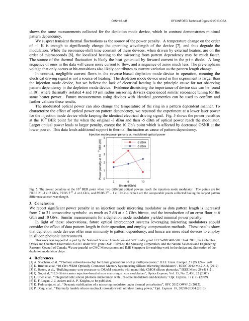
OM2H.6.pdfOFC/NFOEC Technical Digest © 2013 OSAshows the same measurements collected for the depletion mode device, which in contrast demonstrates minimalpattern dependency.We suspect transient thermal fluctuations as the source <strong>of</strong> the power penalty. A temperaturee change on theorder<strong>of</strong> ~1 K is enough to significantly change the operating wavelength <strong>of</strong> the device [7], and thus degrade themodulation. While the resonance-shifttime constantt <strong>of</strong> these devices, when driven by external heaters, are on theorder <strong>of</strong> microseconds [ 8], the localized heating to the microringg from pattern dependency may be much faster.The source<strong>of</strong> the thermal fluctuation is likely the heat generated d by forward current in the p-i-n diode. A longsequence <strong>of</strong> ones in the data will causemore current to flow, and a sequence <strong>of</strong> zeros much less. The pre-emphasisvoltage that only occurs at bit-transitions also likely contributes to current variation as the patternlength change.In contrast, negligible current flows in the reverse-biased depletion mode device in operation, meaning theelectrical driving signal is not a source <strong>of</strong> heating. The depletion mode device used in this experiment is larger thanthe injection mode device, but we believe the lack <strong>of</strong> electrical heating is the principle cause for not observingpattern dependency in the depletion mode device. Evidence dismissing the importance <strong>of</strong> device size can be foundin [8], where thermally isolated 4 and 10 µm radius microring devices experienced similar resonance tuning for thesame heater power. Future measurements using devices with identical geometries can be used to confirmandfurther validate these results.The modulated optical power can also change the temperaturee <strong>of</strong> the ring ina pattern dependent manner. Tocharacterize the effect <strong>of</strong>optical poweron pattern dependency, wee repeated the experiment at a lower laser powerfor the injection mode device while keeping the identical electrical driving signal. Fig. 5 showss the power penaltiesat the 10 -9 BER point for the when the original -3 dBm and thenn -5 dBm <strong>of</strong> optical power reach the modulator.Larger optical power leads to larger penalty, except the 10 Gb/s point which is affected by decreased OSNRat thelower power. This data lends additional support to thermal fluctuation as cause <strong>of</strong>f pattern dependency.Fig. 5. The power penalties att the 10 -9 BER point when two different optical powers reach the injection mode modulator. The pointsare forPRBS 2 -31 -1 at 2 Gb/s, PRBS 2 -23 -1 at 6 Gb/s, and PRBS 2 11 – 1 at 10 Gb/s, which are the comparablee points collected having the largestpatterndifference at each wavelength.3. ConclusionWe report significant power penalty inan injection mode microring modulator as data patternlength is increasedfrom 7 to 31 consecutivee symbols: as much as 2 dBat a 2 Gb/s bitrate, and theintroduction <strong>of</strong> an error floor at 6Gb/s and 10 Gb/s. Similar measurements for a depletion mode modulator yielded minimal power penalty.In light <strong>of</strong> these observations, future optical interconnect systems leveraging microringmodulators shouldconsider the effect <strong>of</strong> data pattern length in their operation, and employ compensation methods.These resultss showthat depletion mode devices <strong>of</strong>fer near immunity to pattern dependency, and hence are more ideal devices to employin silicon photonic interconnects.This work was supported inpart by the National Science Foundation and SRC under grant ECCS-0903406 Corporation, and the Natural Sciences and EngineeringResearch Council <strong>of</strong> Canada. We are grateful to CMC Microsystems and IME Singapore for enabling work in the designand fabrication <strong>of</strong> theSRC Task 2001, the ColumbiaOptics and Quantum Electronics IGERT under NSF grant DGE-1069420, the Samsungdepletion modulation chips.4. References[1] A. Shacham, et al., “Photonic networks-on-chip for future generations <strong>of</strong> chip multiprocessors,” IEEE Trans. Comput. 57 (9) 1246-1260.[2] D. Brunina et al, “10-Gb/s WDM Optically-Connected MemorySystem using Silicon <strong>Microring</strong> <strong>Modulators</strong>”, ECOCC 2012 Mo.2.A.5, (2012)[3] C. Batten, , et al., “Building many-core processor-to-DRAM networks with monolithic CMOS silicon photonics,” IEEE Micro 29 (4) 8-21.[4] Q. Xu, et al, “12.5 Gbit/s carrier injection-based silicon microring silicon modulators”, Optics Express, Vol. 15, No. 2, 430, 22 (2007)[5] L. Chen et al., “Integrated GHz silicon photonic interconnect with µm-scale modulators and detectors,” Opt. Express. 17 (17). (2009).[6] D. F. Logan, J. J. Ackert and A. P. Knights, tobe published.[7] K. Padmaraju, et. al., “Dynamic stabilization <strong>of</strong> a microring modulator under thermal perturbation” ”, OFC 2012 OW4F.2 (2012).[8] P. Dong, et al., "Thermally tunable silicon racetrack resonators with ultralow tuning power," Opt. Express 18, 20298-20304 (2010).