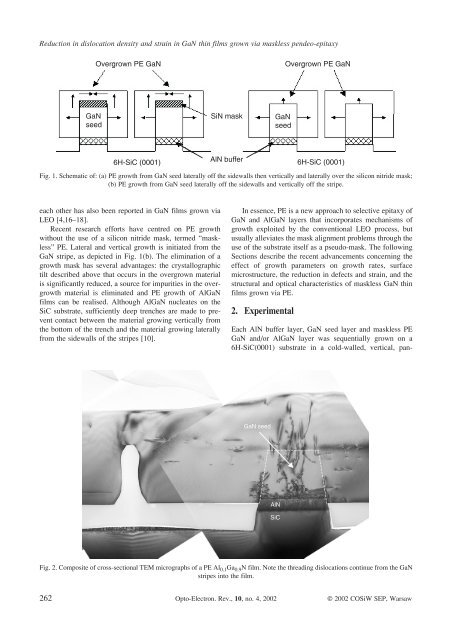
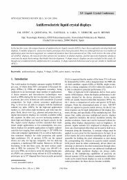
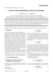
Reduction in dislocation density and strain in GaN thin films grown via maskless pendeo-epitaxyFig. 1. Schematic of: (a) PE growth from GaN seed laterally off the sidewalls then vertically and laterally over the silicon nitride mask;(b) PE growth from GaN seed laterally off the sidewalls and vertically off the stripe.each other has also been reported in GaN films grown viaLEO [4,16–18].Recent research efforts have centred on PE growthwithout the use of a silicon nitride mask, termed “maskless”PE. Lateral and vertical growth is initiated from theGaN stripe, as depicted in Fig. 1(b). The elimination of agrowth mask has several advantages: the crystallographictilt described above that occurs in the overgrown materialis significantly reduced, a source for impurities in the overgrowthmaterial is eliminated and PE growth of AlGaNfilms can be realised. Although AlGaN nucleates on theSiC substrate, sufficiently deep trenches are made to preventcontact between the material growing vertically fromthe bottom of the trench and the material growing laterallyfrom the sidewalls of the stripes [10].In essence, PE is a new approach to selective epitaxy ofGaN and AlGaN layers that incorporates mechanisms ofgrowth exploited by the conventional LEO process, butusually alleviates the mask alignment problems through theuse of the substrate itself as a pseudo-mask. The followingSections describe the recent advancements concerning theeffect of growth parameters on growth rates, surfacemicrostructure, the reduction in defects and strain, and thestructural and optical characteristics of maskless GaN thinfilms grown via PE.2. ExperimentalEach AlN buffer layer, GaN seed layer and maskless PEGaN and/or AlGaN layer was sequentially grown on a6H-SiC(0001) substrate in a cold-walled, vertical, pan-Fig. 2. Composite of cross-sectional TEM micrographs of a PE Al 0.1 Ga 0.9 N film. Note the threading dislocations continue from the GaNstripes into the film.262 Opto-Electron. Rev., 10, no. 4, 2002 © 2002 COSiW SEP, Warsaw
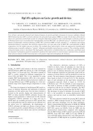
cake-style metalorganic vapour phase epitaxy (MOVPE)system. The 100-nm thick AlN buffer layers and the 1-µmthick GaN seed layers were grown at 20 Torr and plattertemperatures of 1120°C and 1020°C, respectively. The precursorspecies (mass flow rates) of tri-methylaluminum(TMA; 5.4 µmol/min), tri-ethylgallium (TEG; 101 µmol/min) and ammonia (NH 3 ; 0.14 mol/min) were mixed with ahigh-purity H 2 diluent (3 slm) in a two-inch internal diametersleeve located two inches above the substrate.A Ni layer was deposited on patterned photoresiststripes on each GaN seed layer by e-beam evaporation.Etch mask stripes were subsequently produced using standardphotolithography lift-off techniques. An inductivelycoupled plasma (ICP) system and a mixture of Cl 2 andBCl 3 gases were used to etch the unmasked striped regionsthrough the GaN and the AlN and into the near-surface areasof the SiC substrate. The Ni was then removed using a5-min dip in HNO 3 . The remaining GaN seed layer consistedof 2 and 3 µm wide stripes separated by distances of12 and 7 µm, respectively, and oriented along [1120]. Theexposed (1120) sidewalls and the top (0001) face of thestripes were subsequently dipped in 50% hot HCl to cleanthe surface prior to regrowth of the PE layer.The lateral and vertical growth rates of the PE GaNfilms are very sensitive to temperature and the NH 3 /TEG(V/III) molar flow rate ratios. As such, the growth of thesefilms was investigated over the ranges of temperature andTEG flow rates of 1040°C–1100°C and 17–100 µmole/min,respectively. The flow rates of the NH 3 and the H 2 diluentwere maintained at 0.14 mol/min and 3 slm, respectively.The total gas flow into the reactor remained constant for allthe experiments to assure a uniform laminar flow over thesubstrate.Cross-sectional images of the surface microstructure ofthe wing and stripe material were obtained using scanningelectron microscopy (SEM) and were used to calculate thelateral and/or vertical growth rates of these features.Atomic force microscopy (AFM) was employed in the tappingmode to obtain higher resolution micrographs of thegrowth surface as well as the aerial distribution of dislocationsthat terminated at the (0001) surface. Defect characterisationand measurements of the strain via changes inlattice parameter were conducted using the results from onandoff-axis rocking curves and reciprocal space mappingacquired via high-resolution x-ray diffraction (HRXRD).Optical characterisation of spatially resolved (»400 nm)band-edge emission was performed via micro-photoluminescence(PL) at 10 K using a He-Cd (l = 325 nm) laser.Shifts in the frequency of the E2 line measured at 10 K usingan Ar-ion (l = 488 nm) laser coupled to micro-Ramanunit with a spatial resolution of »700 nm, revealed discreteregions of strain in the PE films. Micro-Raman spectra ofthe LO phonon also yielded information regarding the carrierconcentration of the overgrown material. Secondary-ionmass spectroscopy (SIMS) depth pro<strong>file</strong>s were obtainedto determine the presence and concentrations of carbon,oxygen and silicon in the GaN films.3. Results and discussionInvited paper3.1. Pendeo-epitaxial growth and decomposition onGaN(0001) and (1120) surfacesHigh lateral growth rates are desired in both LEO and PEtechniques to achieve rapid coalescence and commerciallyviability. Reported factors that increase the lateral growthrate of GaN films in the [1120] direction from [1100] orientedstripes include growth temperature [12,19], V/III molarflow rate ratio [1,2] and modulation of the NH 3 flowrate [5,9].Figures 3 and 4 are related by the lower case letters ineach and show analytically and pictorially, respectively,the effect of growth temperature for two V/III flow rate ratioson the lateral/vertical GaN growth rate ratios (R). TheV/III ratio was increased from 1323 to 6160 at all temperaturesvia reduction in the TEG flow rate from 101.2µmol/min to 16.7 µmol/min. The most dramatic increase inR occurred for the V/III ratio of 6160 after the growth temperaturewas increased beyond 1060°C, as shown, e.g., inFig. 3(d) and the associated Fig. 4(d). However, the roughnessof the (0001) surface also increased above an R = 10;as seen in the SEM image, Fig. 4(d), of a sample having avalue of R of approximately 24. Additional understandingregarding the changes in the values of R can be obtained byuncoupling the lateral and vertical growth rates and plottingthem as a function of temperature in the manner shownin Fig. 5. Calculation of the growth rates from the SEMcross-sectional micrographs shown in Fig. 4 and additionalmicrographs acquired for the PE GaN films grown at theintermediate temperatures revealed that the lateral growthrate increased with increasing temperature and the verticalgrowth rate either remained constant or decreased for bothV/III ratios. In Fig. 5, the growth rates, both laterally andvertically, are greater for the V/III ratios of 1323 than forthe ratio of 6160 due to the larger amount of TEG used inFig. 3. Ratio of lateral (L)-to-vertical (V) growth rates (R) as afunction of growth temperature and V(NH 3 )/III(TEG) ratio. TheNH 3 flow rate remained constant. Inset shows how a representativevalue of R was calculated for these films. The growth time was 1 hrfor each point.Opto-Electron. Rev., 10, no. 4, 2002 A.M. Roskowski 263