Nanoscale femtosecond spectroscopy for material science and ...
Nanoscale femtosecond spectroscopy for material science and ...
Nanoscale femtosecond spectroscopy for material science and ...

You also want an ePaper? Increase the reach of your titles
YUMPU automatically turns print PDFs into web optimized ePapers that Google loves.
Synthetic Metals 139 (2003) 687–690<strong>Nanoscale</strong> <strong>femtosecond</strong> <strong>spectroscopy</strong> <strong>for</strong> <strong>material</strong><strong>science</strong> <strong>and</strong> nanotechnologyMaria Antonietta Loi ∗ , Enrico Da Como, Roberto Zamboni, Michele MucciniIstituto per lo Studio dei Materiali Nanostrutturati (ISMN), Consiglio Nazionale delle Ricerche CNR,Via P. Gobetti 101, 40129 Bologna, ItalyAbstractThe design <strong>and</strong> implementation of a novel facility to per<strong>for</strong>m ultrafast <strong>spectroscopy</strong> <strong>and</strong> three-dimensional (3D) fabrication at thenanoscale is reported. Single <strong>and</strong> multiphoton <strong>femtosecond</strong> excitation coupled to a laser scanning confocal microscope <strong>and</strong> a photoncounting streak camera system allows to per<strong>for</strong>m photoluminescence (PL) <strong>spectroscopy</strong> with in-plane spatial resolution of the order of100 nm <strong>and</strong> temporal resolution of ∼2 ps. The facility combines high per<strong>for</strong>mance imaging capabilities in 3D with high sensitivity detectionsystem <strong>and</strong> time-resolution of the photoluminescence. Imaging <strong>and</strong> <strong>spectroscopy</strong> are per<strong>for</strong>med on the same spatial position thus allowinga direct correlation of the morphological features with the spectroscopic properties. The use of a laser scanning confocal microscopegives the advantages of far-field microscopy (possible sample perturbation as in the case of near-field technique is prevented) with spatialresolution well below the diffraction limit, <strong>and</strong> fast laser scanning <strong>for</strong> fast data acquisition <strong>and</strong> lower sample photodegradation. A possibleapplication of this optical nano-probe is in the spectroscopic investigation <strong>and</strong> imaging of the active areas of molecular electronic <strong>and</strong>optoelectronic devices, such as TFTs, LEDs <strong>and</strong> PVs cells. The morphology of active layers within working devices can be correlated tofield distributions, charge flows, charge recombination <strong>and</strong> light emission. We show the potential of this novel experimental set-up <strong>for</strong> thestudy of organic, hybrid, biological nanostructures <strong>and</strong> nanodevices.© 2003 Elsevier Science B.V. All rights reserved.Keywords: <strong>Nanoscale</strong> ultrafast <strong>spectroscopy</strong>; Confocal microscopy; Two-photon excitation microscopy; Nanotechnology1. IntroductionConfocal laser microscopy is experiencing intense developmentnot only in the traditional area of cell biology,but also in other scientific <strong>and</strong> technological fields, suchas <strong>material</strong> <strong>science</strong> <strong>and</strong> nanotechnology [1,2], where it canprovide unprecedented probing <strong>and</strong> fabrication tools. Withrespect to near-field microscopy [3], which can reach lateralresolution down to few nanometers [4,5], far-field confocalmicroscopy [6] has a lower lateral resolution that approach100 nm [7]. However, in particular in the laser scanningversion, confocal microscopy <strong>and</strong> <strong>spectroscopy</strong> remainsattractive <strong>for</strong> nanoscale investigations; as it is less invasive<strong>and</strong> perturbing (especially important <strong>for</strong> soft matter), canper<strong>for</strong>m three-dimensional (3D) imaging [6] <strong>and</strong> fast dataacquisition. The latter may become extremely important toprevent sample photodegradation.∗ Corresponding author. Tel.: +39-051-639-8515;fax: +39-051-639-8539.E-mail address: ma.loi@ism.bo.cnr.it (M.A. Loi).In addition, confocal laser microscopy allows straight<strong>for</strong>wardaxial tomography even in the presence of opaque samplesby using two- or three-photon absorption to enhancelaser penetration within the sample [8,9].Laser scanning confocal microscopy <strong>and</strong> <strong>spectroscopy</strong> canbe a key tool <strong>for</strong> <strong>material</strong> <strong>science</strong> <strong>and</strong> nanotechnology, as itmay probe fundamental electronic <strong>and</strong> optical properties atthe relevant nanoscale. A direct correlation of the spectroscopicproperties of <strong>material</strong>s <strong>and</strong> devices with morphologicalfeatures can be achieved at the nanoscale, thus providingfundamental underst<strong>and</strong>ing of nanostructured <strong>material</strong>s <strong>and</strong>devices. In the case of organics, <strong>for</strong> example, evidences areavailable that tailoring the morphological characteristics ofthin films directly affects the per<strong>for</strong>mance <strong>and</strong> working conditionsof optoelectronic devices, such as OLEDs, OTFTs<strong>and</strong> OPVs cells [10,11]. In this view, there is urgent need ofa detailed microscopic underst<strong>and</strong>ing of field distributions,charge flows, charge recombination <strong>and</strong> light emission inthe active layers of devices.In this paper, we report on a novel integrated facility <strong>for</strong>optical probing <strong>and</strong> 3D fabrication at the nanoscale, basedon ultrafast <strong>and</strong> continuous laser excitation, confocal laser0379-6779/$ – see front matter © 2003 Elsevier Science B.V. All rights reserved.doi:10.1016/S0379-6779(03)00265-0
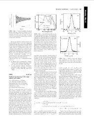
688 M.A. Loi et al. / Synthetic Metals 139 (2003) 687–690scanning microscope, continuous <strong>and</strong> time-resolved detectionof photoluminescence (PL). The facility allows directcorrelation between nano-architectures <strong>and</strong> spectroscopic responsewith in-plane spatial resolution of the order of 100 nm<strong>and</strong> temporal resolution of ∼2 ps.Moreover, the system permits fabrication of three-dimensionalnanostructures via spatially selected photobleachingof photosensitive <strong>material</strong>s or via two-photon initiatedphoto-polymerization [12]. 3D structures can be computerdesigned with a final resolution of the order of 200 nm [13].2. Experimental set-up <strong>and</strong> application to organicnanostructured thin filmsIn Fig. 1 is reported the experimental set-up of thenanoscale <strong>femtosecond</strong> facility based on a confocal laserscanning microscope, a Ti:sapphire <strong>femtosecond</strong>/picosecondlaser, three single line cw lasers (405, 488 <strong>and</strong> 543 nm),three parallel channels <strong>for</strong> integrated PL detection centeredat selected spectral ranges in the visible <strong>and</strong> a streak camera<strong>for</strong> time-resolved PL measurements.The optical microscope is a Nikon Eclipse TE-2000-E inthe inverted configuration equipped with a single pinholeconfocal scanning head. Fig. 2 shows a schematic of theconfocal laser scanning head, whose main components arethe confocal pinhole <strong>and</strong> the galvanometric scanning mirrors.The pinhole is optically conjugated to the focal planeof the microscope <strong>and</strong> cuts the sample luminescence fromabove <strong>and</strong> below the focal plane, thus increasing the overallspatial resolution [6].The galvanometric mirrors provide precision scanningof the laser beam on the sample surface, while the axialtomography is obtained by scanning the sample throughthe focal plane with minimum step of 50 nm. The xyz spatialcontrol of laser excitation allows the imaging of thesample by sequential detection of the photoluminescenceintensity. In order to develop the scanning confocal microscopeas a spectroscopic tool, several dichroic mirrors(Fig. 2) with complementary spectral properties that allowPL spectra measurements in the entire visible rangewere custom designed to be inserted in the scanning head.The three cw excitation lasers are coupled either independentlyor contemporarily into the microscope througha multimode optical fiber, thus permitting simultaneousexcitation of different chromophores <strong>and</strong> electronic excitedstates. Sample imaging is achieved by detectingsample photoluminescence with three independent photomultipliers,each centered in a complementary spectralwindow of the visible range. The independent detectionchannels provide in<strong>for</strong>mation on the spatial location ofchromophores or electronic states emitting at differentwavelengths.The spatial resolution of the photoluminescence imagesdepends on the confocal pinhole diameter, <strong>and</strong> is proportionalto the ratio between the laser excitation wavelength<strong>and</strong> the objective numerical aperture (NA)( λ∗)resolution ∼ 0.37 with λ ∗ = (λ exc λ emiss ) 1/2 (1)NA( )λexcresolution ∼ 0.51(2)NAFig. 1. Schematic of the nanoscale <strong>femtosecond</strong> facility <strong>for</strong> <strong>material</strong> <strong>science</strong> <strong>and</strong> nanotechnology. The system has <strong>femtosecond</strong>, picosecond <strong>and</strong> continuouslaser excitation sources coupled to a confocal laser scanning microscope <strong>and</strong> to a detection set up <strong>for</strong> integrated <strong>and</strong> time-resolved photoluminescencemeasurements. 3D imaging of samples is per<strong>for</strong>med by mapping of one- or two-photon excited photoluminescence with controlled laser scanning. Samplescan be excited simultaneously by three independent laser lines <strong>and</strong> photoluminescence imaging at three selected wavelength ranges can be acquiredsimultaneously. Pulsed excitation switch from the range 700–1000 nm to the range 350–500 nm is achieved by insertion/removal of M1 <strong>and</strong> M2 mirrors.
M.A. Loi et al. / Synthetic Metals 139 (2003) 687–690 689Fig. 2. Schematic of the single pinhole compact confocal scanning head. The incoming laser beam is reflected by the dichroic mirror <strong>and</strong> scanned ontothe sample by two galvanometric mirrors. The sample photoluminescence is collected through the same optical path, being transmitted by the dichroicmirror. The pinhole selects the portion of the sample contributing to the photoluminescence which reaches the detectors.Eq. (1) refers to the theoretical approximation <strong>for</strong> a pinholeaperture smaller than 0.25 Airy units (AU), where 1 AU =(1.22λ exc )/NA while the second is valid <strong>for</strong> aperture rangingfrom 1 Airy unit to infinite aperture [6]. From Eq. (2) byusing oil immersion objective with numerical aperture ashigh as 1.3 <strong>and</strong> excitation wavelength of 400 nm it is possibleto obtain in-plane resolution of ∼160 nm <strong>and</strong> axial resolution(z) of∼480 nm.The facility is further provided with a mode-lockedTi:sapphire <strong>femtosecond</strong>/picosecond laser, pumped at532 nm by a solid state 10 W cw laser. The Ti:sapphirelaser has tunable emission in the range between 700 <strong>and</strong>1000 nm, with pulse duration of ∼100 fs <strong>and</strong> repetition rateof 80 MHz. The pulsed laser is directly coupled into thescanning head with external optics. The set up design issuch to minimize the pulsed laser beam path through transmissionoptics in order to minimize pulse broadening. Thelaser pulse duration is estimated to be of the order of fewhundred <strong>femtosecond</strong> at the microscope focal plane.The second harmonic of the Ti:sapphire laser is used toextend the excitation wavelength in the range 350–500 nm<strong>and</strong> is generated by coupling the Ti:sapphire laser beaminto a -barium borate (BBO) nonlinear crystal. Twoeasy to change optical paths (see Fig. 1) are used <strong>for</strong> the350–500 nm <strong>and</strong> the 700–1000 nm pulsed excitation ranges.The Ti:sapphire fundamental laser emission provides excitationenergy that can be used <strong>for</strong> two-photon excitation(TPE) in organics, while the doubled frequency laser beamis used <strong>for</strong> single photon excitation.By two-photon excitation it is possible to achieve sampleimaging <strong>and</strong> 3D structures nanofabrication with resolution ofabout 200 nm [13]. In this case, the spatial resolution is givenby the sample volume where there is the probability <strong>for</strong> the<strong>material</strong> to absorb coherently two photons of the incominglaser beam. The two-photon absorption is proportional to thesquare of the electromagnetic field intensity, which confinesthe non-linear process in a small portion of the irradiatedspot in the sample [14].An Hamamatsu streak camera system with a temporalresolution of ∼2 ps coupled to a monochromator is usedto spectrally resolve photoluminescence <strong>and</strong> to measure itstime evolution. The output fiber of the confocal microscopeis coupled to the streak camera allowing the association oftime-resolved PL spectra to the selected spatial position onthe sample. The set-up can additionally be used to map, withnanoscale resolution, the emission in light emitting devicesas, e.g. OLEDs. Spatially controlled laser excitation can providecorrelation between action spectra <strong>and</strong> local film morphologyin photovoltaic devices.As an illustrative example of the morphological–spectroscopicin<strong>for</strong>mation which can be obtained with thepresented facility, we consider thin films of conjugated<strong>material</strong>s which are relevant <strong>for</strong> molecular electronics <strong>and</strong>Fig. 3. Confocal photoluminescence image of a 50 nm thick film oftetracene grown by high vacuum sublimation. Sample photoluminescencehas been excited by the second harmonic of the <strong>femtosecond</strong> Ti:sapphirelaser at 400 nm. Lateral dimension of the confocal image is 100 m.
690 M.A. Loi et al. / Synthetic Metals 139 (2003) 687–690Fig. 4. Photoluminescence spectrum of the selected portion of the tetracenefilm indicated in Fig. 3 by the white circle. Photoluminescence excitationconditions are the same used to image the sample, i.e. second harmonicof the <strong>femtosecond</strong> Ti:sapphire laser at 400 nm.optoelectronics. Fig. 3 shows a confocal PL image of atetracene film with 50 nm thickness grown by high vacuumsublimation. The sample has been imaged with a 40times magnification oil immersion objective <strong>and</strong> photoluminescencehas been excited with the second harmonic ofthe Ti:sapphire laser at 400 nm. Detection of the spatiallyresolved PL intensity is per<strong>for</strong>med with the PMT, whosesensitive spectral window is centered at 515 nm. Fig. 4Fig. 5. Time-resolved photoluminescence decay at 525 nm of the portionof tetracene thin film indicated in Fig. 3 by the white circle. Photoluminescenceexcitation conditions are the same used to image the sample<strong>and</strong> to measure the steady state spectrum, i.e. second harmonic of the<strong>femtosecond</strong> Ti:sapphire laser at 400 nm. The inset shows the photoluminescencedecay in logarithmic scale.reports the PL spectrum of the tetracene film originatedfrom the sample area circled in white in Fig. 3. The correspondingPL time decay at 525 nm is given in Fig. 5. Byselecting the spatial position of the spectroscopic analysiswe can directly correlate the morphological features to thephotophysical properties in nanostructured samples.In conclusion, we reported the design <strong>and</strong> implementationof a novel experimental facility that allows to per<strong>for</strong>mnanoscale 3D imaging, ultrafast <strong>spectroscopy</strong>, <strong>and</strong> photonicfabrication at the nanoscale. We discussed the great potentialof this tool when applied to <strong>material</strong> <strong>science</strong> <strong>and</strong> nanotechnology.The presented set-up offers novel opportunities toinvestigate the photophysical properties of organic, hybrid<strong>and</strong> biological nanostructures <strong>and</strong> nanodevices.AcknowledgementsWork supported by the European Communities’ FET-ISTprogram under contract IST-2001-33057, ILO. We thank F.Cicoira, M. Murgia <strong>for</strong> samples preparation, <strong>and</strong> P. Mei <strong>and</strong>T. Bonfiglioli <strong>for</strong> technical support.References[1] F. Koberling, A. Mews, G. Philipp, U. Kolb, I. Potapova, M.Burghard, T. Baschè, Appl. Phys. Lett. 81 (2002) 1116.[2] R. Gronheid, J. Hofkens, F. Koehn, T. Weil, E. Reuther, K. Muellen,F.C. De Schryver, J. Am. Chem. Soc. 124 (2002) 2418.[3] D.W. Pohl, U.Ch. Fischer, U.T. During, J. Microsc. 152 (1988) 853.[4] F. Zenhausern, Y. Martin, H.K. Wickramasinghe, Science 269 (1995)1083.[5] J.D. McNeill, D.B. O’Connor, P.F. Barbara, J. Chem. Phys. 112(2000) 7811.[6] T. Wilson, Confocal Microscopy, Academic Press, London, 1990.[7] M. Schrader, S.W. Hell, H.T.M. van der Voort, Appl. Phys. Lett. 69(1996) 3644.[8] W. Denk, J.H. Strickler, W.W. Webb, Science 248 (1990) 73.[9] S. Maiti, J.B. Shear, R.M. Williams, W.R. Zipfel, W.W. Webb,Science 275 (1997) 530.[10] S.E. Shaheen, C.J. Brabec, N.S. Sariciftci, F. Padinger, T. Fromherz,J.C. Hummelen, Appl. Phys. Lett. 78 (2001) 841.[11] M. Muccini, M. Murgia, F. Biscarini, C. Taliani, Adv. Mater. 13(2001) 335.[12] B.H. Cumpston, S.P. Ananthavel, S. Barlow, D.L. Dyer, J.E.Ehrlich, L.L. Erskine, A.A. Heikal, S.M. Kuebler, I.-Y.S. Lee, D.McCord-Maughon, J. Quin, H. Roeckel, M. Ruml, X.-L. Wu, S.R.Marder, J.W. Perry, Nature Optics Letters 398 (1999) 51.[13] J. Serbin, A. Egbert, A. Ostendorf, B.N. Chichkov, R. Houbertz, G.Domann, J. Schulz, C. Cronauer, L. Froehlich, M. Popall 28 (2003)301.[14] O. Nakamura, Microsc. Res. Tech. 47 (1999) 165.