Design of Low Noise PLL by Improving Supply Sensitivity of VCO ...
Design of Low Noise PLL by Improving Supply Sensitivity of VCO ...
Design of Low Noise PLL by Improving Supply Sensitivity of VCO ...

Create successful ePaper yourself
Turn your PDF publications into a flip-book with our unique Google optimized e-Paper software.
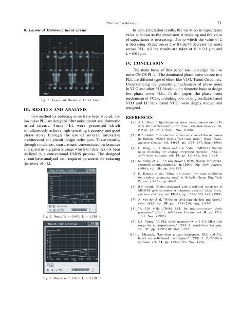
B. Layout <strong>of</strong> Harmonic tuned circuitPatel and Kshirsagar 71In both simulation results, the variation in capacitancevalue is shown as the dimension is reducing and the value<strong>of</strong> capacitance is increasing. Due to which the value <strong>of</strong> Lis decrasing. Reduction in L will help to decrease the noiseacross <strong>PLL</strong>. All the results are taken at W = 0.1 m andL = 0.01 m.Fig. 5. Layout <strong>of</strong> Harmonic Tuned Circuit.III. RESULTS AND ANALYSISTwo method for reducing noise have been studied. Forlow noise <strong>PLL</strong> we designed filter noise circuit and Harmonictuned circuit. Since <strong>PLL</strong> were presented whichsimultaneously achieve high operating frequency and goodphase noise through the use <strong>of</strong> several innovativearchitectural and circuit design techniques. These circuits,through simulation, measurement, demonstrated performanceand speed in a gigahertz range which till date has not beenrealized in a conventional CMOS process. The designedcircuit have analysed with required parameter for reducingthe noise <strong>of</strong> <strong>PLL</strong>.Fig. 6. Nmos W = 0.900, L = 0.120 mIV. CONCLUSIONThe main focus <strong>of</strong> this paper was to design the lownoise CMOS <strong>PLL</strong>. The dominated phase noise source in a<strong>PLL</strong> are different type <strong>of</strong> block like <strong>VCO</strong>, Tuned Circuit etc.Understanding the generating mechanism <strong>of</strong> phase noisein <strong>VCO</strong> and other <strong>PLL</strong> blocks is the theoretic basis to designlow phase noise <strong>PLL</strong>s. In this paper, the phase noisemechanism <strong>of</strong> <strong>VCO</strong>s, including both <strong>of</strong> ring oscillator based<strong>VCO</strong> and LC tank based <strong>VCO</strong>, were deeply studied andanalyzed.REFRENCES[1] A.A. Abidi, "High-frequency noise measurements on FET'swith small dimensions," IEEE Trans. Electron Devices, vol.ED-33, pp. 1801-1805, Nov. (1986).[2] R.P. Jindal, "Hot-electron effects on channel thermal noisein fineline NMOS field-effect transistors," IEEE Trans.Electron Devices, vol. ED-33, pp. 1395-1397, Sept. (1986).[3] B. Wang, J.R. Hellums, and C.G. Sodini, "MOSFET thermalnoise modeling for analog integrated circuits," IEEE J.Solid-State Circuits, vol. 29, pp. 833-835, July (1994).[4] S. Sheng et al., "A low-power CMOS chipset for spreadspectrumcommunications," in ISSCC Dig. Tech. Papers,(1996), vol. 39, pp. 346-347.[5 E. Heaney et al., "Ultra low power low noise amplifiersfor wireless communications," in GaAs-IC Symp. Dig. Tech.Papers, (1993), pp. 49-51.[6] R.P. Jindal, "<strong>Noise</strong> associated with distributed resistance <strong>of</strong>MOSFET gate structures in integrated circuits," IEEE Trans.Electron Devices, vol. ED-31, pp. 1505-1509, Oct. (1984).[7] A. van der Ziel, "<strong>Noise</strong> in solid-state devices and lasers,"Proc. IEEE, vol. 58, pp. 1178-1206, Aug. (1970).[8] "A 320 MHz CMOS <strong>PLL</strong> for microprocessor clockgeneration," IEEE J. Solid-State Circuits, vol. 31, pp. 1715-1722, Nov. (1996).[9] I.A. Young, "A <strong>PLL</strong> clock generator with 5-110 MHz lockrange for microprocessors," IEEE J. Solid-State Circuits,vol. 27, pp. 1599-1607,Nov. 1992.[10] J. Maneatis, "<strong>Low</strong>-jitter process independent DLL and <strong>PLL</strong>based on self-biased techniques," IEEE J. Solid-StateCircuits, vol. 31, pp. 1723-1732, Nov. 1996.Fig. 7. Nmos W = 1.020, L = 0.120 m