PMD in High-Bit-Rate Transmission and Means for Its Mitigation
PMD in High-Bit-Rate Transmission and Means for Its Mitigation
PMD in High-Bit-Rate Transmission and Means for Its Mitigation

You also want an ePaper? Increase the reach of your titles
YUMPU automatically turns print PDFs into web optimized ePapers that Google loves.
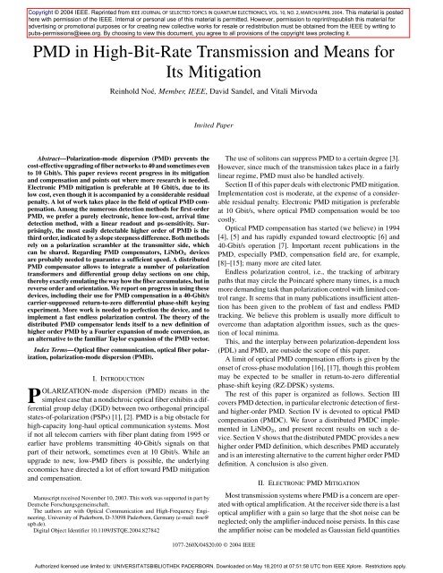
IEEE JOURNAL OF SELECTED TOPICS IN QUANTUM ELECTRONICS, VOL. 10, NO. 2, MARCH/APRIL 2004 341<strong>PMD</strong> <strong>in</strong> <strong>High</strong>-<strong>Bit</strong>-<strong>Rate</strong> <strong>Transmission</strong> <strong>and</strong> <strong>Means</strong> <strong>for</strong><strong>Its</strong> <strong>Mitigation</strong>Re<strong>in</strong>hold Noé, Member, IEEE, David S<strong>and</strong>el, <strong>and</strong> Vitali MirvodaInvited PaperAbstract—Polarization-mode dispersion (<strong>PMD</strong>) prevents thecost-effective upgrad<strong>in</strong>g of fiber networks to 40 <strong>and</strong> sometimes evento 10 Gbit/s. This paper reviews recent progress <strong>in</strong> its mitigation<strong>and</strong> compensation <strong>and</strong> po<strong>in</strong>ts out where more research is needed.Electronic <strong>PMD</strong> mitigation is preferable at 10 Gbit/s, due to itslow cost, even though it is accompanied by a considerable residualpenalty. A lot of work takes place <strong>in</strong> the field of optical <strong>PMD</strong> compensation.Among the numerous detection methods <strong>for</strong> first-order<strong>PMD</strong>, we prefer a purely electronic, hence low-cost, arrival timedetection method, with a l<strong>in</strong>ear readout <strong>and</strong> ps-sensitivity. Surpris<strong>in</strong>gly,the most easily detectable higher order of <strong>PMD</strong> is thethird order, <strong>in</strong>dicated by a slope steepness difference. Both methodsrely on a polarization scrambler at the transmitter side, whichcan be shared. Regard<strong>in</strong>g <strong>PMD</strong> compensators, LiNbO 3 devicesare probably needed to guarantee a sufficient speed. A distributed<strong>PMD</strong> compensator allows to <strong>in</strong>tegrate a number of polarizationtrans<strong>for</strong>mers <strong>and</strong> differential group delay sections on one chip,thereby exactly emulat<strong>in</strong>g the way how the fiber accumulates, but <strong>in</strong>reverse order <strong>and</strong> orientation. We report on progress <strong>in</strong> us<strong>in</strong>g thesedevices, <strong>in</strong>clud<strong>in</strong>g their use <strong>for</strong> <strong>PMD</strong> compensation <strong>in</strong> a 40-Gbit/scarrier-suppressed return-to-zero differential phase-shift key<strong>in</strong>gexperiment. More work is needed to perfection the device, <strong>and</strong> toimplement a fast endless polarization control. The theory of thedistributed <strong>PMD</strong> compensator lends itself to a new def<strong>in</strong>ition ofhigher order <strong>PMD</strong> by a Fourier expansion of mode conversion, asan alternative to the familiar Taylor expansion of the <strong>PMD</strong> vector.Index Terms—Optical fiber communication, optical fiber polarization,polarization-mode dispersion (<strong>PMD</strong>).I. INTRODUCTIONPOLARIZATION-mode dispersion (<strong>PMD</strong>) means <strong>in</strong> thesimplest case that a nondichroic optical fiber exhibits a differentialgroup delay (DGD) between two orthogonal pr<strong>in</strong>cipalstates-of-polarization (PSPs) [1], [2]. <strong>PMD</strong> is a big obstacle <strong>for</strong>high-capacity long-haul optical communication systems. Mostif not all telecom carriers with fiber plant dat<strong>in</strong>g from 1995 orearlier have problems transmitt<strong>in</strong>g 40-Gbit/s signals on thatpart of their network, sometimes even at 10 Gbit/s. While anupgrade to new, low-<strong>PMD</strong> fibers is possible, the underly<strong>in</strong>geconomics have directed a lot of ef<strong>for</strong>t toward <strong>PMD</strong> mitigation<strong>and</strong> compensation.Manuscript received November 10, 2003. This work was supported <strong>in</strong> part byDeutsche Forschungsgeme<strong>in</strong>schaft.The authors are with Optical Communication <strong>and</strong> <strong>High</strong>-Frequency Eng<strong>in</strong>eer<strong>in</strong>g,University of Paderborn, D-33098 Paderborn, Germany (e-mail: noe@upb.de).Digital Object Identifier 10.1109/JSTQE.2004.827842The use of solitons can suppress <strong>PMD</strong> to a certa<strong>in</strong> degree [3].However, s<strong>in</strong>ce much of the transmission takes place <strong>in</strong> a fairlyl<strong>in</strong>ear regime, <strong>PMD</strong> must also be h<strong>and</strong>led actively.Section II of this paper deals with electronic <strong>PMD</strong> mitigation.Implementation cost is moderate, at the expense of a considerableresidual penalty. Electronic <strong>PMD</strong> mitigation is preferableat 10 Gbit/s, where optical <strong>PMD</strong> compensation would be toocostly.Optical <strong>PMD</strong> compensation has started (we believe) <strong>in</strong> 1994[4], [5] <strong>and</strong> has rapidly exp<strong>and</strong>ed toward electrooptic [6] <strong>and</strong>40-Gbit/s operation [7]. Important recent publications <strong>in</strong> the<strong>PMD</strong>, especially <strong>PMD</strong>, compensation field are, <strong>for</strong> example,[8]–[15]; many more are cited later.Endless polarization control, i.e., the track<strong>in</strong>g of arbitrarypaths that may circle the Po<strong>in</strong>caré sphere many times, is a muchmore dem<strong>and</strong><strong>in</strong>g task than polarization control with limited controlrange. It seems that <strong>in</strong> many publications <strong>in</strong>sufficient attentionhas been given to the problem of fast <strong>and</strong> endless <strong>PMD</strong>track<strong>in</strong>g. We believe this problem is usually more difficult toovercome than adaptation algorithm issues, such as the questionof local m<strong>in</strong>ima.This, <strong>and</strong> the <strong>in</strong>terplay between polarization-dependent loss(PDL) <strong>and</strong> <strong>PMD</strong>, are outside the scope of this paper.A limit of optical <strong>PMD</strong> compensation ef<strong>for</strong>ts is given by theonset of cross-phase modulation [16], [17], though this problemmay be expected to be smaller <strong>in</strong> return-to-zero differentialphase-shift key<strong>in</strong>g (RZ-DPSK) systems.The rest of this paper is organized as follows. Section IIIcovers <strong>PMD</strong> detection, <strong>in</strong> particular electronic detection of first<strong>and</strong>higher-order <strong>PMD</strong>. Section IV is devoted to optical <strong>PMD</strong>compensation (<strong>PMD</strong>C). We favor a distributed <strong>PMD</strong>C implemented<strong>in</strong> LiNbO , <strong>and</strong> present recent results on such a device.Section V shows that the distributed <strong>PMD</strong>C provides a newhigher order <strong>PMD</strong> def<strong>in</strong>ition, which describes <strong>PMD</strong> accurately<strong>and</strong> is an <strong>in</strong>terest<strong>in</strong>g alternative to the current higher order <strong>PMD</strong>def<strong>in</strong>ition. A conclusion is also given.II. ELECTRONIC <strong>PMD</strong> MITIGATIONMost transmission systems where <strong>PMD</strong> is a concern are operatedwith optical amplification. At the receiver side there is a lastoptical amplifier with a ga<strong>in</strong> so large that the shot noise can beneglected; only the amplifier-<strong>in</strong>duced noise persists. In this casethe amplifier noise can be modeled as Gaussian field quantities1077-260X/04$20.00 © 2004 IEEEAuthorized licensed use limited to: UNIVERSITATSBIBLIOTHEK PADERBORN. Downloaded on May 18,2010 at 07:51:58 UTC from IEEE Xplore. Restrictions apply.
342 IEEE JOURNAL OF SELECTED TOPICS IN QUANTUM ELECTRONICS, VOL. 10, NO. 2, MARCH/APRIL 2004Fig. 1.Electrical <strong>PMD</strong> mitigation by quantized feedback. Note that the noise amplitude <strong>in</strong>creases with the signal amplitude.Fig. 2.Calculated OSNR penalty versus normalized DGD.<strong>in</strong> phase <strong>and</strong> <strong>in</strong> quadrature to the wanted signal. The photocurrentis proportional to the squared magnitude of the field, <strong>and</strong>has there<strong>for</strong>e a probability density function. If noise is small<strong>and</strong> optical filter<strong>in</strong>g is tight, then the decision threshold of thephotocurrent is ideally near 1/4 of the full signal sw<strong>in</strong>g becausethe decision threshold of the optical field would be near 1/2 ofthe signal sw<strong>in</strong>g. Usually 1/3 is implemented because of nonidealmodulator ext<strong>in</strong>ction. A compilation of the mathematicalsteps is given <strong>in</strong> [18].If the eye diagram is fully closed, <strong>for</strong> example, because thetransmitted power is launched with equal powers <strong>in</strong>to both PSPs<strong>and</strong> the DGD is one bit duration, l<strong>in</strong>ear electronic equalizerscannot help. As an example, <strong>for</strong> the electronic <strong>PMD</strong> mitigation,consider there<strong>for</strong>e a decision feedback equalizer (DFE), whichcan help even <strong>in</strong> such cases. In Fig. 1 the left part schematicallyshows the received eye diagram. The decision marg<strong>in</strong> is fairlysmall because the DGD is close to one bit duration. The rightpart shows the same eye diagram, but decomposed depend<strong>in</strong>g onwhether the previous symbol was a zero or a one. The decisionfeedback can place the effective decision levels at or near theoptimum positions.While the eye open<strong>in</strong>g penalty <strong>in</strong> the decomposed eye diagramsis less than 3 dB <strong>in</strong> Fig. 1, the optical signal-to-noise ratio(OSNR) penalty is a lot worse. Especially the preced<strong>in</strong>g ones atthe right side are difficult to work with. This is because only truezeros have low noise, <strong>and</strong> nonzero signals are accompanied by alot of noise. Fig. 2 shows calculated OSNR penalties. When theDGD equals one bit duration , the residual penalty with DFEcan surpass 9 dB. The number of degrees-of-freedom (DOFs)of the distributions is approximately equal to 2 (<strong>in</strong>-phase <strong>and</strong>quadrature noise) times 2 (polarizations) times the ratio of theFig. 3.M<strong>in</strong>imum DOP versus DGD <strong>for</strong> different pulse shapes.optical b<strong>and</strong>pass filter width divided by twice the electrical lowpassfilter width (at least equal to one). Much fewer than eightDOFs are not well realizable. The true residual penalty can belower than predicted here, because a nonideal <strong>in</strong>tensity modulatorext<strong>in</strong>ction ratio can cause a basel<strong>in</strong>e penalty that maskssome of the total penalty. For example, an ext<strong>in</strong>ction ratio of13 dB causes a penalty of at least 1.5 dB.Also, add<strong>in</strong>g a transversal filter be<strong>for</strong>e the DFE improves thesituation. Thirdly, thermal noise can never completely neglected<strong>and</strong> also adds a basel<strong>in</strong>e penalty.Not surpris<strong>in</strong>gly, a number of experiments with electronic<strong>PMD</strong> mitigation circuits has shown penalties on the order of severaldecibels [19]–[25], especially when accompanied by EDFAnoise. DFE operation beyond 10 Gbit/s is possible, but difficult[25]. In total, electronic <strong>PMD</strong> mitigation circuits are very attractiveat 10 Gbit/s, where the cost of optical <strong>PMD</strong> compensatorsis too big an obstacle. Whether they can be implementedat 40 Gbit/s rema<strong>in</strong>s to be seen; this will at least be very difficult.The two next sections will there<strong>for</strong>e concentrate on <strong>PMD</strong>compensation <strong>in</strong> the optical doma<strong>in</strong>.III. <strong>PMD</strong> DETECTIONA. Optical <strong>PMD</strong> Detection MethodsS<strong>in</strong>ce <strong>PMD</strong> happens <strong>in</strong> the optical fiber, it is straight<strong>for</strong>wardto detect it <strong>in</strong> the optical doma<strong>in</strong>, be<strong>for</strong>e the photodetector destroyspolarization <strong>in</strong><strong>for</strong>mation. Several related methods havemostly been employed: Kikuchi has proposed to monitor the degree-of-polarization(DOP) [26]. Later, Rosenfeldt et al. haveadded polarization scrambl<strong>in</strong>g at the transmitter side becausethis allows one to obta<strong>in</strong> a more <strong>in</strong><strong>for</strong>mative readout, <strong>in</strong>clud<strong>in</strong>ghigher order <strong>PMD</strong> [27]. Fig. 3 shows a simulated DOP readoutAuthorized licensed use limited to: UNIVERSITATSBIBLIOTHEK PADERBORN. Downloaded on May 18,2010 at 07:51:58 UTC from IEEE Xplore. Restrictions apply.
NOÉ et al.: <strong>PMD</strong> IN HIGH-BIT-RATE TRANSMISSION 343Fig. 4.Measurement setup <strong>and</strong> projections of measured output polarization trace of “tennis ball” polarization scrambler.as a function of DGD <strong>for</strong> various pulse shapes. The readoutis proportional to the DGD, but only if the pulse edges areshorter than the DGD. For RZ pulses the readout is somewhatambiguous.Rosenfeldt et al. have also reported on a polarimeter placedbeh<strong>in</strong>d a tunable, frequency-swept optical b<strong>and</strong>pass filter [28].Recently, Möller et al. have replaced the tunable filter by an angledfiber Bragg grat<strong>in</strong>g <strong>in</strong> view of polarimetry [29]. Photodetectorarrays provide a parallel readout of the frequency-dependentStokes parameters. In pr<strong>in</strong>ciple this is a low-cost solutionthat should allow one to construct such a spectral polarimeter,cover<strong>in</strong>g a whole WDM b<strong>and</strong>. However, <strong>in</strong> practice it is morecommon to monitor the signal beh<strong>in</strong>d a <strong>PMD</strong> compensator thatis dedicated to one WDM channel, <strong>and</strong> this would mean thatone spectral polarimeter is needed <strong>for</strong> each WDM channel. Frequency-<strong>in</strong>dependent<strong>in</strong>l<strong>in</strong>e polarimeters can also be fabricatedbased on fiber Bragg grat<strong>in</strong>gs [30].The efficiency of all these methods is of course <strong>in</strong>creased ifmeasurements take place at several positions, <strong>for</strong> example, atthe <strong>in</strong>put, at an <strong>in</strong>ternal tap, <strong>and</strong> at the output of an optical <strong>PMD</strong>compensator [27], [31], [15].S<strong>in</strong>ce cost seems to be the most important decision criterionnowadays, the authors prefer electronic <strong>PMD</strong> detectionmethods. Some of them need polarization scrambl<strong>in</strong>g just likea few optical methods [27], [31].B. Polarization Scrambl<strong>in</strong>gPolarization scrambl<strong>in</strong>g is an ancillary science to <strong>PMD</strong> detection.A variety of optical <strong>PMD</strong> detection techniques [27],[31] need polarization scramblers. In most cases it is possibleto share one scrambler by many WDM channels, so the costis not prohibitive. Polarization-<strong>in</strong>dependent scramblers can beconstructed [32], but the time-b<strong>and</strong>width product is so large thatthey are not very attractive: Either the <strong>PMD</strong> detection <strong>in</strong>tervalmust be very long or the electronic process<strong>in</strong>g b<strong>and</strong>width ofthe (optical or electronic) <strong>PMD</strong> detection device must be quitelarge.We have there<strong>for</strong>e implemented a polarization scrambler withthe lowest possible time-b<strong>and</strong>width product [32]. It works <strong>for</strong> apair of fixed orthogonal <strong>in</strong>put polarizations. This means that theWDM channel signals must be comb<strong>in</strong>ed at the transmitter sidewith polarization-ma<strong>in</strong>ta<strong>in</strong><strong>in</strong>g components.Let the time-variable scrambler output polarization <strong>and</strong> a PSPof a subsequent fiber be denoted by the normalized Stokes vectors. We drop the time dependence <strong>and</strong> <strong>in</strong>troduce theaverag<strong>in</strong>g operator . The covariance matrix of the scrambleroutput polarization iswhere denotes transposition. Ideally, should vanish <strong>and</strong>should become equal to 1/3 times the identity matrix. Obviouslyits three eigenvalues are all equal to 1/3. One solution isthe Stokes vectorwhere is the scrambl<strong>in</strong>g frequency. A s<strong>in</strong>gle electroopticwaveplate [33] on a commercially available X-cut, Z-propagationLiNbO chip has been used with circular <strong>in</strong>put polarization,“rotat<strong>in</strong>g” orientation, <strong>and</strong> periodically time-variable retardationto implement such a scrambler. The upper signs <strong>in</strong> (2) werechosen. Fig. 4 shows projections of Po<strong>in</strong>caré sphere traces,taken at the device output at a low speed. They look like thevulcanization l<strong>in</strong>e of a tennis ball. The eigenvalues of werevery close to the ideal values of 1/3, with relative deviationsfrom their mean of just 1.7%. When the wavelength wastuned, the lowest eigenvalue stayed above 0.28 over more than40 nm b<strong>and</strong>width.C. Electronic <strong>PMD</strong> Detection MethodsAmong the electronic methods <strong>for</strong> first-order <strong>PMD</strong> detection,we favor the arrival time detection scheme [34], [36]. In thepresence of <strong>PMD</strong>, the polarization modulation caused by thescrambler is accompanied by an arrival time modulation. If theslow PSP of a first-order <strong>PMD</strong> medium with a DGD is givenby the normalized Stokes vector , then the pulse arrivaltime isThe variance ofisWith (1) <strong>and</strong> (2), the resultis obta<strong>in</strong>ed. Therms value is directly proportional to the DGD. This is agreat advantage because even small DGDs can be accuratelydetected.(1)(2)Authorized licensed use limited to: UNIVERSITATSBIBLIOTHEK PADERBORN. Downloaded on May 18,2010 at 07:51:58 UTC from IEEE Xplore. Restrictions apply.
344 IEEE JOURNAL OF SELECTED TOPICS IN QUANTUM ELECTRONICS, VOL. 10, NO. 2, MARCH/APRIL 2004Fig. 5.First-order <strong>PMD</strong> detection us<strong>in</strong>g tennis ball scrambler <strong>and</strong> arrival time detection. M = motorized endless fiber-optic polarization trans<strong>for</strong>mers.Fig. 6. <strong>PMD</strong> detection readout <strong>for</strong> tennis ball scrambler <strong>and</strong> arrival time detection scheme <strong>in</strong> a 40-Gbit/s CSRZ-DPSK setup. Solid curves correspond to lowest<strong>and</strong> highest readouts caused by motorized polarization trans<strong>for</strong>mers. Associated 6 one st<strong>and</strong>ard deviation <strong>in</strong>tervals are <strong>in</strong>dicated by “0” <strong>and</strong> allow one to assessthe sensitivity.The purely electronic first-order <strong>PMD</strong> detection takes place<strong>in</strong> a setup accord<strong>in</strong>g to Fig. 5. In our first experiments a40-Gbit/s NRZ transmission system was used. The tennis ballscrambler was operated with a fundamental scrambl<strong>in</strong>g frequencyof 417 kHz. Precharacterized polarization-ma<strong>in</strong>ta<strong>in</strong><strong>in</strong>gfiber (PMF) pieces were <strong>in</strong>serted as <strong>PMD</strong> devices under test.In order to <strong>in</strong>clude any uncontrollable polarization <strong>in</strong>fluence<strong>in</strong>clud<strong>in</strong>g PDL, slow motorized polarization trans<strong>for</strong>mers (M)were added be<strong>for</strong>e <strong>and</strong> after the PMF. The clock <strong>and</strong> datarecovery <strong>in</strong> the optical receiver features a clock phase detector.Together with a voltage-controlled oscillator (VCO) <strong>and</strong> aloop filter, a proportional-<strong>in</strong>tegral controller (PI), it <strong>for</strong>ms aphase-locked loop (PLL). The clock recovery PLL tracks the<strong>PMD</strong>-<strong>in</strong>duced arrival time fluctuations. If it is fast enough,then the signal at the VCO <strong>in</strong>put is proportional to the temporalderivative of the arrival time modulation. It is sufficient to <strong>in</strong>tegratethis signal, <strong>and</strong> to measure the rms value of the <strong>in</strong>tegral,thereby obta<strong>in</strong><strong>in</strong>g . The measurement <strong>in</strong>terval was onescrambl<strong>in</strong>g period, 2.4 s. The sensitivity, where the readoutm<strong>in</strong>us one st<strong>and</strong>ard deviation was more than the backgroundreadout plus one st<strong>and</strong>ard deviation, was about 0.88–1.35 ps[32]. Very similar readouts result <strong>for</strong> RZ modulation. A 210-kmtransmission <strong>and</strong> <strong>PMD</strong> compensation experiment was alsoconducted [36]. There was normal PDL <strong>in</strong> the l<strong>in</strong>k. No attemptsto suppress it were made here, nor <strong>in</strong> the next experiment.Recently the arrival time detection scheme was also tested<strong>for</strong> carrier-suppressed return-to-zero (CSRZ)-DPSK signals. Inthat case the receiver front end consisted of an <strong>in</strong>terferometer<strong>and</strong> two photodetectors, <strong>and</strong> it was connected to the differential<strong>in</strong>puts of the clock-<strong>and</strong>-data recovery. The exact setup is shownlater <strong>in</strong> Fig. 16. The obta<strong>in</strong>ed readouts are very similar to thoseobta<strong>in</strong>ed <strong>for</strong> NRZ <strong>in</strong>tensity modulation <strong>in</strong> [32]. Fig. 6 shows afairly l<strong>in</strong>ear readout from about 1 to 19 ps. The sensitivity wasassessed to be 1.2 ps.Quite <strong>in</strong>terest<strong>in</strong>gly, arrival time detection of <strong>PMD</strong> is alsopossible <strong>in</strong> polarization multiplexed transmission systemsus<strong>in</strong>g the RZ signal <strong>for</strong>mat [35]–[37]. The big advantage hereis that no scrambler is necessary at all because it is replacedby a differential phase modulation between the two orthogonalpolarization channels, which <strong>in</strong> turn is realized by a smalllaser frequency modulation comb<strong>in</strong>ed with a differential delayof the two polarizations be<strong>for</strong>e they are modulated. A <strong>PMD</strong>detection sensitivity of 150 fs has been achieved <strong>in</strong> a 4.8- smeasurement <strong>in</strong>terval, <strong>and</strong> RZ polarization division multiplextransmission over 212 km with <strong>PMD</strong> compensation becamepossible.Among the earliest reported electronic methods <strong>for</strong> <strong>PMD</strong> detectionis the power measurement <strong>in</strong> b<strong>and</strong>pass portions of thephotodetected electric signal [5]–[7]. S<strong>in</strong>ce <strong>PMD</strong> is generally alow-pass effect, it is sufficient <strong>for</strong> <strong>PMD</strong> compensation to try tomaximize the high-frequency components of the electric signal.No scrambler is needed, but the readout <strong>for</strong> small DGDs riseswith the square of the DGD.<strong>PMD</strong> can also be detected by threshold scann<strong>in</strong>g [38] <strong>in</strong> anextra decision circuit, or by read<strong>in</strong>g the FEC raw errors. Thesedigital methods are relatively easy to implement but suffer fromspeed penalties, s<strong>in</strong>ce it takes extra time to filter out the quantizationnoise, compared to an analog detection technique.Table I summarizes the properties of the most important optical<strong>and</strong> electrical first-order <strong>PMD</strong> detection methods. ArrivalAuthorized licensed use limited to: UNIVERSITATSBIBLIOTHEK PADERBORN. Downloaded on May 18,2010 at 07:51:58 UTC from IEEE Xplore. Restrictions apply.
NOÉ et al.: <strong>PMD</strong> IN HIGH-BIT-RATE TRANSMISSION 345TABLE IHOW TO DETECT FIRST-ORDER <strong>PMD</strong>time detection possesses most advantages <strong>and</strong> can be realizedwith commercially available technology.<strong>High</strong>er order <strong>PMD</strong> can also be detected electrically, to somedegree. Francia et al. have reported that a <strong>PMD</strong> vector that rotates<strong>in</strong> the Stokes space as a function of optical frequency generatesasymmetric (lead<strong>in</strong>g or trail<strong>in</strong>g) overshoot <strong>in</strong> detectedNRZ signals [39].Accord<strong>in</strong>g to our <strong>in</strong>vestigations [32], the asymmetric distortionis due to third-order <strong>PMD</strong> <strong>and</strong> is characterized by asteepness difference between ris<strong>in</strong>g <strong>and</strong> fall<strong>in</strong>g electrical signalslopes, while second-order <strong>PMD</strong> causes pulse distortions witha front-to-back mirror symmetry. To see this it is sufficient topass an optical data signal through field transfer functions equalto(second-order chromatic dispersion, symmetricdistortion) <strong>and</strong>(third-order chromatic dispersion,asymmetric distortion; see also [40]). In effect, the Taylorexpansion of a circular trajectory must be of <strong>in</strong>f<strong>in</strong>ite order to becorrect. So there is not only second- but also a lot of third-order<strong>PMD</strong>. The effect can only be understood to be of second order(but not to be due to second-order <strong>PMD</strong>) if one takes a <strong>PMD</strong>model with two cascaded DGD sections.The important th<strong>in</strong>g about the asymmetric distortions withslope steepness difference, caused by third-order <strong>PMD</strong>, is thatthey can be detected more sensitively than symmetric overshoot,caused by second-order <strong>PMD</strong>, see Fig. 21 of [32].To discuss a very similar situation more <strong>in</strong> detail, we need to<strong>in</strong>troduce now DGD profiles. The <strong>PMD</strong> vector has a lengthequal to the DGD <strong>and</strong> po<strong>in</strong>ts <strong>in</strong> the direction of a pr<strong>in</strong>cipal stateof-polarization<strong>in</strong> the three-dimensional normalized Stokesspace. If DGD sections are cascaded, the overall <strong>PMD</strong> vectoris given the sumof <strong>in</strong>dividual <strong>PMD</strong> vectors. The are referred to the <strong>in</strong>put of thewhole cascade, whereas are the local <strong>in</strong>dividual <strong>PMD</strong>vectors. is the product of all 3 3 rotation matrices, whichrepresent the retarders (<strong>in</strong>clud<strong>in</strong>g DGD sections) preced<strong>in</strong>g theDGD section . Plott<strong>in</strong>g the sequence of <strong>in</strong> such a way thatthe tail of starts from the head of results <strong>in</strong> a DGDprofile. <strong>Its</strong> endpo<strong>in</strong>t is given by . More details <strong>and</strong> examplesof measured DGD profiles are given <strong>in</strong> [32], [7], <strong>and</strong> [37].After compensation of first-order <strong>PMD</strong>, the DGD profileorig<strong>in</strong> <strong>and</strong> endpo<strong>in</strong>t must co<strong>in</strong>cide (at the optical carrierfrequency) because this means that the first-order <strong>PMD</strong> iszero. The result<strong>in</strong>g DGD profile will most likely consist of aloop or a similar closed trajectory shown <strong>in</strong> Fig. 7(left). Thenearly parabolic trajectory is the position of the <strong>PMD</strong> vectoras a function of frequency. The l<strong>in</strong>ear motion (LM) meanssecond-order <strong>PMD</strong>. The quadratic (<strong>for</strong>th <strong>and</strong> back) motion(QM) is <strong>in</strong> this approximation due to third-order <strong>PMD</strong>. Andhere, as <strong>for</strong> any other DGD profiles, it is the projection (PQM)of the quadratic motion QM along the <strong>in</strong>put polarization(arrow) that determ<strong>in</strong>es the amount of asymmetric overshoot,not second-order <strong>PMD</strong>. The correspond<strong>in</strong>g simulated eyediagram is shown <strong>in</strong> Fig. 7(b). The auxiliary l<strong>in</strong>es underl<strong>in</strong>e theslope steepness difference.The presence of DGD profile loops, which exhibit second<strong>and</strong>third- <strong>and</strong> all higher orders of <strong>PMD</strong>, has been detected <strong>in</strong>the 40-Gbit/s transmission setup of Fig. 8. The signal passed a<strong>PMD</strong> emulator (<strong>PMD</strong>E) <strong>and</strong> compensator (<strong>PMD</strong>C). The <strong>for</strong>merconsists of two mechanical polarization trans<strong>for</strong>mers (M1, M2),each of which is followed by a DGD section. The latter hasthe same structure but uses electrooptic -cut, -propagationLiNbO polarization trans<strong>for</strong>mers (E1, E2). At the receiver sidethere was arrival time detection. The <strong>PMD</strong>C was controlled asto m<strong>in</strong>imize first-order <strong>PMD</strong>. In addition, a slope steepness differencedetector acted on the photodetected signal. It was builton a ceramic substrate with a differentiator <strong>and</strong> two oppositelypoled one-way rectifiers. The usable frequency range was up toGHz <strong>and</strong> turned out to be acceptable. The sum of the tworectified signals represents the slope steepness difference.Experimentally obta<strong>in</strong>ed eye diagrams [41] are shown <strong>in</strong>Fig. 9, displayed with negative polarity, <strong>and</strong> recorded whilethe scrambler was stopped. For the eye diagrams at the bottomthe third-order <strong>PMD</strong> QM is parallel or antiparallel to the <strong>in</strong>putpolarization.The 2.4- s scrambl<strong>in</strong>g period was also chosen <strong>for</strong> slopesteepness difference measurement. In order to maximize higherorder <strong>PMD</strong>, the controller was first set so that it tried tomaximize the rms slope steepness difference by E1, E2. Themanual polarization trans<strong>for</strong>mer M2 was also adjusted with thesame aim. Six cases were <strong>in</strong>vestigated, where the subsequentsections had DGDs of 0 ps (only one manual, no electroopticpolarization trans<strong>for</strong>mer, essentially no PDL), 0 0 0 0ps (back-to-back, with PDL just as <strong>in</strong> all follow<strong>in</strong>g cases), 2.24 4 2.2 ps, 6.25 4 4 6.25 ps, 6.25 6.256.25 6.25 ps, <strong>and</strong> 6.25 19 22.8 6.25 ps, respectively.Nearly flat, rhomboid-shaped DGD profiles are expected, withareas of 0, 0, 8.8, 25, 39, <strong>and</strong> 261 ps , respectively. To givean example, the associated second-order <strong>PMD</strong> <strong>for</strong> the 6.256.25 6.25 6.25 ps case is 78 ps . S<strong>in</strong>ce the setup wasalso <strong>in</strong>fluenced by PDL ( 1 dB), ma<strong>in</strong>ly from E1, E2, theworst case was assessed by adjust<strong>in</strong>g M1 <strong>for</strong> smallest readout.This does not change the rhomboid; it just reorients it <strong>in</strong> the<strong>PMD</strong> vector space. The rms slope difference readouts wererecorded as well as their st<strong>and</strong>ard deviations. After this thecontroller was switched <strong>in</strong> each case to m<strong>in</strong>imize the rms slopedifference readout, while M1, M2 were left unchanged. Value<strong>and</strong> st<strong>and</strong>ard deviation were aga<strong>in</strong> recorded. In Fig. 10 the solidl<strong>in</strong>es are readout values <strong>and</strong> the “ ” signs (sometimes hardlydiscernible) <strong>in</strong>dicate one st<strong>and</strong>ard deviation error <strong>in</strong>tervals.Authorized licensed use limited to: UNIVERSITATSBIBLIOTHEK PADERBORN. Downloaded on May 18,2010 at 07:51:58 UTC from IEEE Xplore. Restrictions apply.
346 IEEE JOURNAL OF SELECTED TOPICS IN QUANTUM ELECTRONICS, VOL. 10, NO. 2, MARCH/APRIL 2004(a)(b)Fig. 7. DGD profile <strong>for</strong> vanish<strong>in</strong>g first-order <strong>PMD</strong>. Output arrows of DGD profile are not shown <strong>for</strong> easier visibility. Correspond<strong>in</strong>g eye diagram exhibits slopesteepness difference.Fig. 8.40-Gbit/s transmission setup with first- <strong>and</strong> third-order <strong>PMD</strong> detection <strong>and</strong> <strong>PMD</strong> compensation.Fig. 9. 40-Gbit/s eye patterns back-to-back (top left), with unequalsteepnesses of ris<strong>in</strong>g <strong>and</strong> fall<strong>in</strong>g slopes (bottom) <strong>and</strong> with unequal curvatures(all except back-to-back). Polarity is negative. <strong>Transmission</strong> took place <strong>in</strong> thesetup of Fig. 8, which was configured to have a DGD profile like <strong>in</strong> Fig. 7,with 6.25 + 6.25 + 6.25 + 6.25 ps of DGD <strong>in</strong> four sections, but the scramblerwas stopped.Between maximized rhomboid areas of 8.8 <strong>and</strong> 39 ps , a roughproportionality of the readout was found as expected. It isseen that between the smallest of the maximized rhomboidareas (8.8 ps ) <strong>and</strong> the maximized back-to-back case thereis a readout difference of several st<strong>and</strong>ard deviations. Theback-to-back case with reduced PDL <strong>and</strong> without <strong>PMD</strong>C (only1 0 ps rema<strong>in</strong>ed) was aga<strong>in</strong> a lot better. So, the large PDLhad an <strong>in</strong>fluence on the setup but even <strong>in</strong> the worst case it waspossible to detect the negligibly small DGD profile rhomboidFig. 10. Slope steepness difference readout versus DGD profile loop area.Lower curve results when controller tries to achieve zero DGD profile area.2.2 4 4 2.2 ps with<strong>in</strong> just 2.4 s. The compensator wasable to essentially close it, as well as all larger DGD profileloops. First-order <strong>PMD</strong> was also compensated at all times.A simultaneous factor measurement was not tried becausethreshold scann<strong>in</strong>g <strong>in</strong>fluences the arrival time detection, <strong>and</strong>thermal drift <strong>in</strong> the DGD sections of the <strong>PMD</strong>E made it difficultto ma<strong>in</strong>ta<strong>in</strong> a certa<strong>in</strong> measurement condition over a longer time.Nevertheless, the assessed <strong>PMD</strong> situations resulted <strong>in</strong> particularlydistorted eye diagrams (under the condition that first-order<strong>PMD</strong> was essentially elim<strong>in</strong>ated).Authorized licensed use limited to: UNIVERSITATSBIBLIOTHEK PADERBORN. Downloaded on May 18,2010 at 07:51:58 UTC from IEEE Xplore. Restrictions apply.
NOÉ et al.: <strong>PMD</strong> IN HIGH-BIT-RATE TRANSMISSION 347IV. OPTICAL <strong>PMD</strong> COMPENSATIONA. Devices <strong>and</strong> MethodsBe<strong>for</strong>e specializ<strong>in</strong>g on one <strong>PMD</strong> compensation device <strong>and</strong>method we review here some work <strong>in</strong> this field.Inside an optical <strong>PMD</strong>C with cascaded DGD sections eachof its polarization trans<strong>for</strong>mers must be able to endlessly trans<strong>for</strong>many <strong>in</strong>put polarization <strong>in</strong>to a pr<strong>in</strong>cipal state-of-polarizationof the subsequent differential group delay section [7].Endless track<strong>in</strong>g means that polarization fluctuations may atany po<strong>in</strong>t <strong>in</strong> the fiber l<strong>in</strong>k go around the Po<strong>in</strong>caré spheremore than once, possibly an <strong>in</strong>f<strong>in</strong>ite number of times. Thisis a much more difficult task than polarization control withlimited control range: For any polarization trans<strong>for</strong>mer, thetrack<strong>in</strong>g of certa<strong>in</strong> small polarization fluctuations will requirelarge drive signal changes. For example, when an electroopticSoleil–Bab<strong>in</strong>et compensator [33] (rotatable waveplate with adjustableretardation) with circular <strong>in</strong>put polarization reaches aretardation angle of while the output polarization marchesstraight through the po<strong>in</strong>t of circular retardation, then it mustchange its orientation angle by ; else the retardation angle<strong>and</strong> the required driv<strong>in</strong>g voltages will keep <strong>in</strong>creas<strong>in</strong>g, eventuallydestroy<strong>in</strong>g the device.Polarization trans<strong>for</strong>mers with retarders hav<strong>in</strong>g fixed eigenmodesare more complicated to control. Procedures are necessarywhere a retardation is typically reset by 2 under cooperationof other retarders to keep the output polarization unchanged[34]. Fiber squeezers <strong>and</strong> most k<strong>in</strong>ds of liquid crystal cells belongto this class. The track<strong>in</strong>g speed that can be achieved ism<strong>in</strong>imum if the absolute value of the retardation is not stable.Stability is usually not specified by manufacturers. Even whenthe retardation is stable the safe endless track<strong>in</strong>g speed is just0.033 rad/iteration [42]. We there<strong>for</strong>e see the potential of suchretarders <strong>for</strong> <strong>PMD</strong> compensation as quite critical. For comb<strong>in</strong>ationwith a high-speed controller, we believe the response timeshould be on the order of 5 s or less.All polarization trans<strong>for</strong>mers can be operated as endless deviceseven without stable retardation if there are many of them.However, the speed penalty paid <strong>for</strong> this simplification is dramatic.A workhorse <strong>for</strong> a lot of experimental <strong>PMD</strong> compensationwork are electrooptic waveplates <strong>in</strong> -cut, -propagationLiNbO . These devices are not birefr<strong>in</strong>gent <strong>and</strong> have a wideoptical b<strong>and</strong>width. The response is <strong>in</strong>creased by a f<strong>in</strong>ite bufferlayer isolation, but is there<strong>for</strong>e not fully <strong>in</strong>stantaneous.In addition to endless control of one variable polarizaitonwith an electrooptic Soleil–Bab<strong>in</strong>et compensator [33] twoSoleil–Bab<strong>in</strong>et compensators [43] or three waveplates [44]have been used to trans<strong>for</strong>m any <strong>in</strong>put <strong>in</strong>to any output polarization.Devices where the waveguide birefr<strong>in</strong>gence is tuned outcompletely by a slight off-axis propagation can be operated withlow offset voltages. But the waveguide exhibits a reciprocalcircular retardation. Another issue is dc drift [45]: Chargesgenerated by the pyroelectric effect are separated under the<strong>in</strong>fluence of a static external electric field, thereby weaken<strong>in</strong>gthis field <strong>in</strong>side <strong>and</strong> near the waveguide. Ion migration <strong>in</strong> thebuffer layer <strong>and</strong>/or conductivity disturbances of the crystalFig. 11. 20-Gbit/s eye diagrams (a) back-to-back, (b) with emulator <strong>and</strong> idle<strong>PMD</strong>Cs (unusually good here), (c) with emulator <strong>and</strong> work<strong>in</strong>g <strong>PMD</strong>Cs, <strong>and</strong> (d)with <strong>PMD</strong>Cs alone.Fig. 12. Elementary <strong>in</strong>-phase <strong>and</strong> quadrature mode converter (one section) <strong>in</strong>x-cut, y-propagation LiNbO .cause a similar effect. DC drift limits are not known or at leastnot specified <strong>for</strong> commercial -cut, -propagation LiNbOpolarization trans<strong>for</strong>mers. The dc drift lets the retardationoffset calibration drift slowly with time, <strong>and</strong> this is the biggestproblem.Polarization controllers made of any other materials thanLiNbO are less suitable <strong>in</strong> our op<strong>in</strong>ion.B. Distributed <strong>PMD</strong> CompensatorRegard<strong>in</strong>g cost <strong>and</strong> space, the <strong>in</strong>tegratability of several polarizationtrans<strong>for</strong>mers <strong>and</strong> DGD sections <strong>in</strong>to one device is decisive.This requirement, <strong>and</strong> most others, are best fulfilled <strong>in</strong> adistributed <strong>PMD</strong>C. In a preparatory attempt a weakly polarization-ma<strong>in</strong>ta<strong>in</strong><strong>in</strong>gfiber with a total DGD of 77 ps was twisted at64 positions. This resulted <strong>in</strong> successful <strong>PMD</strong> compensation at20 Gbit/s [7].Later the pr<strong>in</strong>ciple was implemented <strong>in</strong> an -cut, -propagationLiNbO chip. At 20 Gbit/s, 10 20 ps of DGD were compensatedby two cascaded distributed LiNbO <strong>PMD</strong>Cs with atotal DGD of 43 ps [46]. Correspond<strong>in</strong>g eye diagrams are shown<strong>in</strong> Fig. 11. The device was also tested at 40 Gbit/s [47].In the follow<strong>in</strong>g we will concentrate on recent progress withthese devices [48], [49]. Fig. 12 shows a basic polarization trans<strong>for</strong>mer,an <strong>in</strong>-phase <strong>and</strong> quadrature mode converter as proposedby Heismann <strong>and</strong> Ulrich [50]. Several or many of them are cascaded<strong>in</strong> a distributed <strong>PMD</strong>C. Comb-shaped mode converterelectrodes are distributed along a birefr<strong>in</strong>gent waveguide.The electrode period equals the TE-TM beat length(22 m at 1550 nm). This mode converter may be called aSoleil–Bab<strong>in</strong>et analog SBA [7] because of the analogyto a Soleil–Bab<strong>in</strong>et compensator: What the Soleil–Bab<strong>in</strong>etcompensator does with circular, the SBA can do with horizontal/verticalpolarizations. It is described by a Jones matrixAuthorized licensed use limited to: UNIVERSITATSBIBLIOTHEK PADERBORN. Downloaded on May 18,2010 at 07:51:58 UTC from IEEE Xplore. Restrictions apply.
348 IEEE JOURNAL OF SELECTED TOPICS IN QUANTUM ELECTRONICS, VOL. 10, NO. 2, MARCH/APRIL 2004or a 3 3 rotation matrix ( Mueller submatrix), shown <strong>in</strong> (3)at the bottom of the page, respectively. An SBA <strong>in</strong>troducesan angle equal to its retardation between the <strong>PMD</strong> vectordirections of a preced<strong>in</strong>g <strong>and</strong> a follow<strong>in</strong>g DGD section, therebyrotat<strong>in</strong>g the subsequent rest of the DGD profile by . Angledef<strong>in</strong>es the phase shift between an unconverted <strong>and</strong> amode-converted wave <strong>and</strong> can be called an orientation angle.An SBA retardation of a DGD is represented by a phaseshifter PS with Jones <strong>and</strong> rotation matricesrespectively, where is the optical angular frequency. Thewhole distributed <strong>PMD</strong>C is approximately described by theJones or rotation matrix product<strong>PMD</strong>C PS SBA (4)The product must be executed from left to right with descend<strong>in</strong>g<strong>in</strong>dex while the light passes the SBAs <strong>and</strong> PSs <strong>in</strong>ascend<strong>in</strong>g order . A longitud<strong>in</strong>ally variable pattern of <strong>in</strong>-phasevoltages <strong>and</strong> quadrature voltages (Fig. 12) couples TE<strong>and</strong> TM modes. Us<strong>in</strong>g a constant , we can writeNote that it holds <strong>and</strong> .A pigtailed <strong>PMD</strong>C was electrooptically <strong>in</strong>vestigated. It hadpairs of <strong>in</strong>-phase <strong>and</strong> quadrature electrodes, each segmentbe<strong>in</strong>g 1.27 mm long. The total <strong>PMD</strong> was23 ps, which is good <strong>for</strong> 40-Gbit/s <strong>PMD</strong> compensation. The<strong>PMD</strong>C was operated with a horizontal <strong>in</strong>put polarization <strong>in</strong> thewaveguide. A polarimeter was connected to the <strong>PMD</strong>C output.Consider the case when all voltages except those of segmentare zero. With <strong>PMD</strong>C given by its Jones or its rotation matrix,the output polarization state can be expressed by the Jones ornormalized Stokes vector<strong>PMD</strong>C(5)<strong>PMD</strong>C (6)respectively. Hereare phase shifts. If they aremodulo 2 unequal, then the waveguide is nonuni<strong>for</strong>m. Fourvoltage pairswere appliedsequentially to each of the electrodes <strong>in</strong> section , <strong>and</strong> theoutput polarization state was measured. Equations (5) <strong>and</strong> (6)allowed one to determ<strong>in</strong>e <strong>and</strong> . Per<strong>for</strong>mance was best atFig. 13. (Top) Polarization change ' <strong>and</strong> its orientation (o) <strong>and</strong> (b) orientationerror 0 (+; solid l<strong>in</strong>e) <strong>for</strong> V +jV =20V. Po<strong>in</strong>t i =17, whereboth electrodes had <strong>in</strong>ternal shorts to ground, is omitted.nm, where varied somewhat as a function of butnot too much (Fig. 13).Waveguide nonuni<strong>for</strong>mity can decrease the conversion efficiencyof long mode converters. Indeed, varied unusuallymuch due to errors which occurred <strong>in</strong> the production of thisparticular device. So, if a number of adjacent <strong>in</strong>-phase electrodeswere connected <strong>in</strong> parallel, <strong>and</strong> likewise <strong>for</strong> quadratureelectrodes, then a low mode conversion efficiency would result,especially <strong>for</strong> where adjacent differ by about .Apart from improved fabrication, the only way to combat thisis to subdivide the mode converters <strong>in</strong>to fairly short sections,which was done here. However, it has been argued that a largenumber of electrode voltages cannot be controlled sufficientlyfast.In <strong>PMD</strong> compensation algorithms, it is common to dither variouselectrode voltages, one at a time, <strong>and</strong> to optimize themby a multidimensional gradient search us<strong>in</strong>g one or more controlcriteria. For a maximum voltage of 55 V ( V m), awaveguide length of 4–6 mm will be needed <strong>for</strong> full modeconversion, <strong>and</strong> it is there<strong>for</strong>e possible to reduce the numberof control variables below 2 . A straight<strong>for</strong>ward approach isto specify, say, four “discrete” polarization trans<strong>for</strong>mers at 0,4 /2, <strong>and</strong> 3 /4, where is the chip length. Due to the previouscalibration process, just two control variables are requiredper polarization trans<strong>for</strong>mation, which is the physically necessarym<strong>in</strong>imum. Such a <strong>PMD</strong>C needs voltages but just eight(3)Authorized licensed use limited to: UNIVERSITATSBIBLIOTHEK PADERBORN. Downloaded on May 18,2010 at 07:51:58 UTC from IEEE Xplore. Restrictions apply.
NOÉ et al.: <strong>PMD</strong> IN HIGH-BIT-RATE TRANSMISSION 349control variables, <strong>and</strong> is four times more variable than a <strong>PMD</strong>Cfeatur<strong>in</strong>g one commercial -cut, -propagation LiNbO device.The latter requires up to 16 control variables <strong>for</strong> its eight waveplates,but a reduction of the number of control variables is alsoconceivable there.An alternative approach employs a number of spatial Fouriercoefficients(7)of retardation or mode coupl<strong>in</strong>g as control variables. The required<strong>in</strong>verse Fourier trans<strong>for</strong>m <strong>and</strong> multiplication can be implemented<strong>in</strong> an FPGA <strong>for</strong> fast executionFig. 14. Po<strong>in</strong>caré sphere meridians generated by SBA where the retardationvaries from zero (uncritical “pole,” ”TE”) to almost (critical “pole,” ”TM”)with various orientations. Coord<strong>in</strong>ate system rotation is arbitrary.For a distributed <strong>PMD</strong> compensator, the DGD profile is astraight rod as long as no voltages are applied. The Fourier coefficientcauses a bend or loop, <strong>and</strong> with a spiralof the DGD profile. The coefficients permit a precise control ofthe DGD profile shape. Optimiz<strong>in</strong>g the low-order coefficientsmore often than the high-order ones may improve the mean<strong>PMD</strong> track<strong>in</strong>g speed. Some 38 control variables or so (real <strong>and</strong>imag<strong>in</strong>ary parts of) may be sufficient<strong>for</strong> a 96-mm-long chip. If the center of gravity of the coefficientspectrum, rms-averaged over extended times, is not near, there may be a static phase mismatch. To overcome it,one may correct the chip temperature: A temperature change byK will translate the center of gravity from to zero<strong>for</strong> a 96-mm-long chip. The sign depends on the def<strong>in</strong>ition of<strong>in</strong>-phase versus quadrature.Note, however, that at the chip <strong>in</strong>put an extra polarizationtrans<strong>for</strong>mation, <strong>in</strong>dependent of the Fourier coefficients, shouldpreferably be implemented, <strong>in</strong> order to orient the waveguideDGD as soon as possible <strong>in</strong> such a direction that <strong>PMD</strong> is compensated.At the experimental side we have, <strong>for</strong> a start, optimized thecontrol per<strong>for</strong>mance of one SBA. Six mode converter cells (sections)were used, four of which were sufficient <strong>for</strong> a halfwaveSBA operation (full mode conversion). After calibration the sections<strong>for</strong>m a s<strong>in</strong>gle retarder, which depends only on total retardation<strong>and</strong> total orientation as parameters.A PSP, say, TE, is fed <strong>in</strong>to the polarization trans<strong>for</strong>mer. Thedevice was <strong>in</strong>itially operated as a rotat<strong>in</strong>g halfwave SBA, <strong>and</strong> theoutput polarization (near TM) was recorded with a polarimeter.After proper amplitude adjustment of the s<strong>in</strong>usoidal voltages,the output polarization stayed with<strong>in</strong> a circle hav<strong>in</strong>g a radius ofjust 0.05 rad on the Po<strong>in</strong>caré sphere. Fig. 14 shows output polarizationswhen the SBA retardation was varied from zero to almost<strong>for</strong> various SBA orientations. They converge fairly well<strong>in</strong> one po<strong>in</strong>t, which is essential <strong>for</strong> endless polarization track<strong>in</strong>g.Accord<strong>in</strong>g to our experience, such a good accuracy was notachievable with electrooptic waveplates <strong>in</strong> -cut, -propagationLiNbO from two vendors.Next a mov<strong>in</strong>g target polarization, which the polarizationcontroller has to track, was def<strong>in</strong>ed by software. Only thedistance (on the Po<strong>in</strong>caré sphere) between the actual polarization,measured by a slow polarimeter, <strong>and</strong> the target was usedFig. 15. Misalignment angle distributions dur<strong>in</strong>g worst case polarizationtrack<strong>in</strong>g with a polarimeter (2) <strong>and</strong> dur<strong>in</strong>g r<strong>and</strong>om polarization track<strong>in</strong>g us<strong>in</strong>ga polarization division multiplex <strong>in</strong>terference signal (—).<strong>in</strong> the control algorithm. Virtually all possible polarizationstates <strong>and</strong> trajectories were <strong>in</strong>vestigated but extreme care wastaken to scrut<strong>in</strong>ize the behavior at <strong>and</strong> near the “pole” of TMpolarization. In 30 most critical great circle trajectories acrossthe poles, the worst displacement from the wanted trajectorywas 0.125 rad (Fig. 15). Most measurements had deviations0.04 rad. The track<strong>in</strong>g speed was 0.012 rad/iteration.In order to get rid of the slow polarimeter, a polarizationdivision multiplex signal was set up, <strong>and</strong> the <strong>in</strong>terchannel<strong>in</strong>terference was monitored as apolarization error signal [51].Fig. 15 — shows the misalignment angle distributions obta<strong>in</strong>edwhile r<strong>and</strong>om polarization variations are be<strong>in</strong>g tracked.These were generated by motorized endlessly rotat<strong>in</strong>g fibercoils. The track<strong>in</strong>g speed was 1.3 rad/s or 0.002 rad/iteration(one iteration ms). The worst case misalignment was0.13 rad. Note, however, that endless track<strong>in</strong>g is a worst casescenario that happens rarely. The <strong>in</strong>stantaneous (non endless)track<strong>in</strong>g speed is more than 100 times higher: signal acquisitionfrom anywhere on the Po<strong>in</strong>caré sphere occurs <strong>in</strong> iterationsor so.The slower permissible endless track<strong>in</strong>g per iteration,compared to the previous case <strong>and</strong> compared to the 0.033 rad/iteration <strong>in</strong> [42], is believed to be due to a nonrectangular electroopticstep response of the device. It is caused by a higherconductivity of the buffer layer compared to the LiNbO .More work needs to be done to shorten the electroopticstep response. Alternatively, the response may be electricallyAuthorized licensed use limited to: UNIVERSITATSBIBLIOTHEK PADERBORN. Downloaded on May 18,2010 at 07:51:58 UTC from IEEE Xplore. Restrictions apply.
350 IEEE JOURNAL OF SELECTED TOPICS IN QUANTUM ELECTRONICS, VOL. 10, NO. 2, MARCH/APRIL 2004Fig. 16.40-Gbit/s transmission setup with first- <strong>and</strong> third-order <strong>PMD</strong> detection <strong>and</strong> <strong>PMD</strong> compensation.equalized. At present the track<strong>in</strong>g speed is heavily limited bydeliberately imposed algorithmic constra<strong>in</strong>ts, which could bereleased if the step response were fast <strong>and</strong> rectangular. Thisis expected to be a key to faster track<strong>in</strong>g. The execution timeper iteration can probably cut down to 50 s by a suitablehardware ef<strong>for</strong>t.The dc drift problem observed <strong>for</strong> -cut, -propagation devicesmust also be discussed here. For r<strong>and</strong>om polarization variationsthe voltages needed to control a distributed <strong>PMD</strong>C willhave zero means. This should <strong>in</strong> pr<strong>in</strong>ciple avoid all dc drift. But<strong>in</strong> reality polarization varations may not be as r<strong>and</strong>om as required.However, if a halfwave SBA with slowly rotat<strong>in</strong>g orientationangle is added at the <strong>in</strong>put of the <strong>PMD</strong>C, a differentialphase TE-TM shift is generated. In order to ma<strong>in</strong>ta<strong>in</strong> the desiredDGD profile, the SBA orientations <strong>in</strong> the rest of the distributed<strong>PMD</strong>C must rotate at twice this rate. This can also be accomplishedautomatically dur<strong>in</strong>g the control process. As a consequence,all driv<strong>in</strong>g voltages will be dc-free even if the <strong>PMD</strong>scenario is static [48].Recently, this distributed LiNbO <strong>PMD</strong>C was tested <strong>in</strong> a40-Gbit/s CSRZ-DPSK transmission setup (Fig. 16), similar tothat <strong>in</strong> [52]. Arrival time detection was implemented; <strong>for</strong> resultssee Fig. 6. For <strong>PMD</strong> compensation, the “tennis ball” scrambledsignal was transmitted over available fiber, 33 km of DSF, <strong>and</strong>1 km of SSMF. At the receiv<strong>in</strong>g end there were two DGD sections,<strong>in</strong>serted between three motorized fiber-coil-type endlesspolarization trans<strong>for</strong>mers. The distributed <strong>PMD</strong>C was operatedas a four-section <strong>PMD</strong>C with polarization trans<strong>for</strong>mers atpositions 0.1, 0.35, 0.55, <strong>and</strong> 0.75 , where is the full chiplength ( 23 ps of DGD). A controller processed the arrivaltime signal <strong>and</strong> adjusted the driv<strong>in</strong>g voltages <strong>for</strong> m<strong>in</strong>imumresidual <strong>PMD</strong>. A total of 48 voltages was used, which could<strong>in</strong> the future be controlled by just eight degrees-of-freedom asdescribed above.Measured spectra at the output of the <strong>in</strong>tegrator are displayed<strong>in</strong> Fig. 17, here with DGD sections equal to 8.6 <strong>and</strong> 6.6 ps,respectively. When <strong>PMD</strong> compensation is on, the arrival timesignal is typically 30 dB lower than when it is stopped, <strong>in</strong>dicat<strong>in</strong>ga 30-fold DGD reduction. The multiples one, two, <strong>and</strong>three of the fundamental frequency of 417 kHz are expected tobe found <strong>for</strong> the “tennis ball” curve of the scrambled polarizationon the Po<strong>in</strong>caré sphere. <strong>High</strong>er harmonics were also observedhere, but their amplitudes are unnecessarily <strong>in</strong>creased bythe fact that the <strong>in</strong>tegrator was not a true <strong>in</strong>tegrator <strong>and</strong> had aconstant ga<strong>in</strong> beyond 2 MHz. The higher harmonics present nosignificant disadvantage.Fig. 17. 40-Gbit/s CSRZ-DPSK transmission. Spectra at <strong>in</strong>tegrator outputwith <strong>PMD</strong>C stopped or runn<strong>in</strong>g.The back-to-back receiver sensitivity (without scrambler,fiber, DGD sections, <strong>PMD</strong>C) at the <strong>in</strong>put connector of an opticalpreamplifier equals 32.0 dBm at a BER equal to 10 . DPSKeye pattern monitor<strong>in</strong>g us<strong>in</strong>g an oscilloscope was not possible<strong>in</strong> the <strong>PMD</strong>-compensated setup, because the photodetectedsignals need to be connected to the clock <strong>and</strong> data recovery.However, measured factors <strong>for</strong> various configurations aregiven <strong>in</strong> Fig. 18, us<strong>in</strong>g 2–10-s-long count<strong>in</strong>g <strong>in</strong>tervals <strong>for</strong> eachBER value. The various values belong<strong>in</strong>g to a particularconfiguration were obta<strong>in</strong>ed <strong>for</strong> different sett<strong>in</strong>gs of the fiberpolarization controllers, <strong>in</strong> the quest of best <strong>and</strong> worst cases.Note that the scrambler alone reduces the back-to-backfactor from 29.5 dB (measured separately) to 23.7 dB. Thisis ma<strong>in</strong>ly due to PDL <strong>in</strong> the photodiodes: the longer the BERcount<strong>in</strong>g <strong>in</strong>tervals were, the later the extrapolation began, <strong>and</strong>the better was the factor. So, most given factors are likelyto because the noise probability density function falls off moresharply than that of Gaussian noise. Two DGD sections hav<strong>in</strong>g6.6 <strong>and</strong> 8.6 ps of DGD, <strong>in</strong> addition to scrambler, <strong>PMD</strong>C, <strong>and</strong>34 km of fiber, resulted <strong>in</strong> factors 20 dB.The <strong>PMD</strong>C was also tested dynamically by activat<strong>in</strong>g themotorized fiber polarization controllers. Operation was usuallyerror-free. Occasional errors are believed to be due to higherorder <strong>PMD</strong>, which was not detected here.The bottom l<strong>in</strong>e is that the distributed <strong>PMD</strong>C:• is a natural compensator <strong>for</strong> any <strong>PMD</strong>, as will also be seen<strong>in</strong> Section V;• can be operated with a m<strong>in</strong>imum number of control variables,even if the waveguide is unusually <strong>in</strong>homogeneous;• can be expected to solve the 40-Gbit/s <strong>PMD</strong>C problemonce it is fabricated <strong>in</strong> a commercial fab.Authorized licensed use limited to: UNIVERSITATSBIBLIOTHEK PADERBORN. Downloaded on May 18,2010 at 07:51:58 UTC from IEEE Xplore. Restrictions apply.
NOÉ et al.: <strong>PMD</strong> IN HIGH-BIT-RATE TRANSMISSION 351Fig. 18.40-Gbit/s CSRZ-DPSK transmission with distributed <strong>PMD</strong> compensation: Q-factors measured <strong>for</strong> various configurations.V. HIGHER ORDER <strong>PMD</strong> DEFINITIONA. Taylor Expansion of <strong>PMD</strong> Vector (TEPV)The def<strong>in</strong>ition of first-order <strong>PMD</strong> is undisputed. Poole <strong>and</strong>Wagner have searched those PSPs that will, to first order, notvary as a function of optical frequency at the output of a fiber,<strong>and</strong> have found that they exhibit a DGD [1]. Alternatively onecan determ<strong>in</strong>e the polarization-dependent small-signal <strong>in</strong>tensitymodulation transfer function of a fiber, <strong>and</strong> will f<strong>in</strong>d maximum<strong>and</strong> m<strong>in</strong>imum delays, hence, a DGD between orthogonal twopolarizations, which are the PSPs [7], [53], [54].Regard<strong>in</strong>g higher order <strong>PMD</strong>, almost all previous work onits def<strong>in</strong>ition concerns the familiar truncated Taylor expansionof the <strong>PMD</strong> vector (TEPV). It is easy to calculate the <strong>PMD</strong>vector derivatives from the Jones matrix. The opposite path hasrecently been opened by Heismann [55]. The advantages of ahigher order <strong>PMD</strong> def<strong>in</strong>ition by the TEPV are the follow<strong>in</strong>g.• Easy analytical calculation of higher <strong>PMD</strong> orders• Addition/subtraction of second-order <strong>PMD</strong> to the fiberchromatic dispersion. The same holds <strong>for</strong> other orders of<strong>PMD</strong> <strong>and</strong> chromatic dispersion.• Relation of third-order <strong>PMD</strong> to slope steepness differencesof NRZ signals.<strong>Its</strong> key disadvantages are the follow<strong>in</strong>g.• No direct relation to physical fiber parameters exists.• The true frequency-dependent trajectory of the DGDvector <strong>in</strong> the Stokes space would be described by sumsof s<strong>in</strong>usoids with arguments that depend l<strong>in</strong>early onfrequency. But s<strong>in</strong>usoids are not well approximatedby a Taylor series. Inevitably, an <strong>in</strong>f<strong>in</strong>ite DGD will bepredicted far off the optical carrier frequency.Second-order <strong>PMD</strong> is usually classified with respect to the directionof first-order <strong>PMD</strong> [56]. This is good to discuss statistics.However, like <strong>for</strong> the third-order <strong>PMD</strong> discussed <strong>in</strong> SectionIII-C, its effect on received eye patterns is better describedwhen it is discussed with respect to the signal polarization: Depend<strong>in</strong>gon whether second-order <strong>PMD</strong> is parallel or antiparallelto the <strong>in</strong>put polarization, it will add <strong>and</strong>/or subtract to fiber chromaticdispersion.B. Sequence of DGD Sections (SDGD)Most <strong>PMD</strong> simulation is carried out by assum<strong>in</strong>g a sequenceof cascaded DGD sections (SDGD), because it is widelyaccepted that an <strong>in</strong>f<strong>in</strong>ite number of r<strong>and</strong>omly cascaded sectionsproduces “natural” <strong>PMD</strong>. A f<strong>in</strong>ite SDGD can also be used <strong>for</strong><strong>PMD</strong> description [7]. A restricted 3-section variant <strong>for</strong> effectsup to the second order was proposed by Shtaif et al. [57].Möller [58] has po<strong>in</strong>ted out that the structure of a cascade ofDGD sections can be obta<strong>in</strong>ed by a layer-peel<strong>in</strong>g algorithm[59]. We have implemented this algorithm <strong>and</strong> have obta<strong>in</strong>edexperimental DGD profiles of simple <strong>PMD</strong> media, <strong>in</strong>clud<strong>in</strong>gour distributed <strong>PMD</strong> compensator <strong>in</strong> several configurations[32]. Important advantages of the SDGD method are thefollow<strong>in</strong>g.• Easy graphical display of DGD profile.• Build<strong>in</strong>g a <strong>PMD</strong> emulator with SDGD is much easier thanbuild<strong>in</strong>g one <strong>for</strong> the TEPV with adjustable orders of first<strong>and</strong>higher order <strong>PMD</strong> [60].• It emulates what a real fiber typically does, which is notevident <strong>for</strong> TEPV-based higher order <strong>PMD</strong> emulators.A disadvantage of the <strong>PMD</strong> def<strong>in</strong>ition by a SDGD is thepotentially large number of unknowns. A modification of thescheme might <strong>in</strong>volve choos<strong>in</strong>g a number of DGD sections,<strong>for</strong> example, all with equal, <strong>in</strong>itially unknown lengths, <strong>and</strong>then f<strong>in</strong>d<strong>in</strong>g their length <strong>and</strong> orientations that describe the<strong>PMD</strong> medium best. Obviously a s<strong>in</strong>gle DGD section describesfirst-order <strong>PMD</strong> alone. Two DGD sections describe this,plus the fairly typical <strong>in</strong>terplay between higher orders of theTaylor-approximated <strong>PMD</strong> vector. The total DGD is constant,which is rem<strong>in</strong>iscent of [56], where it has been shown thatsecond-order <strong>PMD</strong> parallel to first-order <strong>PMD</strong> is a lot weakerthan that perpendicular to it. The typical slope steepnessdifference, caused by third-order <strong>PMD</strong>, can easily be observedeven <strong>in</strong> two DGD sections. More accurate <strong>PMD</strong> model<strong>in</strong>g ispossible with three or more DGD sections.While all this makes sense, we discuss <strong>in</strong> the follow<strong>in</strong>g a relatedtechnique to describe higher order <strong>PMD</strong>.C. Fourier Expansion of Mode Coupl<strong>in</strong>g (FEMC)The direction change between adjacent DGD sections is theretardation of a mode converter. Seen by an observer who looks<strong>in</strong> the direction of the preced<strong>in</strong>g DGD section, this directionchange occurs up/down or right/left. This amounts to <strong>in</strong>-phaseor quadrature mode coupl<strong>in</strong>g between local PSPs. If the numberof DGD sections approaches <strong>in</strong>f<strong>in</strong>ity, mode coupl<strong>in</strong>g becomescont<strong>in</strong>uous. We po<strong>in</strong>t out that it is possible to describe a <strong>PMD</strong>Authorized licensed use limited to: UNIVERSITATSBIBLIOTHEK PADERBORN. Downloaded on May 18,2010 at 07:51:58 UTC from IEEE Xplore. Restrictions apply.
352 IEEE JOURNAL OF SELECTED TOPICS IN QUANTUM ELECTRONICS, VOL. 10, NO. 2, MARCH/APRIL 2004Fig. 19. DGD profile of reference (exemplary <strong>PMD</strong> medium) cascaded with <strong>in</strong>verted FEMC structure (which thereby <strong>for</strong>ms a <strong>PMD</strong> equilizer). Scal<strong>in</strong>g unit isone DGD section length of the reference structure.medium by a Fourier expansion of mode coupl<strong>in</strong>g (FEMC) asfollows.1) A frequency-<strong>in</strong>dependent mode conversion at the fiber<strong>in</strong>put. This is described by two parameters, <strong>for</strong> example,retardation <strong>and</strong> orientation.2) A total DGD.3) A frequency-<strong>in</strong>dependent mode conversion at the fiberoutput. In the general case a mode conversion (two parameters,as at the <strong>in</strong>put) <strong>and</strong> a differential phase shift(one more parameter) are needed. In total this means thatthere is a frequency-<strong>in</strong>dependent elliptical retarder at theoutput.4) Complex Fourier coefficients (7) of mode coupl<strong>in</strong>galong the birefr<strong>in</strong>gent medium, which exhibits the abovementionedtotal DGD only <strong>in</strong> the absence of mode conversion.Among these four items, the first three simply describe firstorder<strong>PMD</strong>, <strong>and</strong> this has been po<strong>in</strong>ted out by many authors. Onlythe fourth item makes it a FEMC. If there is mode coupl<strong>in</strong>g,the DGD profile will bend. Bends at discrete positions wouldcorrespond to the SDGD model. Fourier coefficients describeDGD profile bend<strong>in</strong>g <strong>in</strong> a cont<strong>in</strong>uous manner (Fig. 19).As mentioned, the zero-order coefficient coils the DGDprofile. Whether coil<strong>in</strong>g occurs up/down or right/left or <strong>in</strong> a mixof these cases depends on the phase angle of . The coil<strong>in</strong>gradius is <strong>in</strong>versely proportional to the magnitude of this coefficient.Other will w<strong>in</strong>d a spiral when they occur alone.comb<strong>in</strong>ed with can result <strong>in</strong> a <strong>for</strong>th-<strong>and</strong>-back bend<strong>in</strong>g ofthe DGD profile.The number of real parameters needed to describe <strong>PMD</strong> bythe three mentioned methods is listed <strong>in</strong> Table II. In all casesthree extra parameters must generally be added to specify a frequency-<strong>in</strong>dependentelliptical retarder at the fiber output. Onlythe order 1, correspond<strong>in</strong>g to first-order <strong>PMD</strong>, is identical <strong>for</strong>all methods.The TEPV needs three vector components <strong>in</strong> the Stokes space<strong>for</strong> each <strong>PMD</strong> order. Maximum <strong>PMD</strong> order covered <strong>and</strong> methodorder are equal only here.TABLE IIORDER AND NUMBER OF REAL PARAMETERS IN HIGHER ORDER<strong>PMD</strong> DEFINITION METHODSThe SDGD needs the two parameters of an SBA, plus onetotal DGD, <strong>for</strong> the first order. Each additional order is def<strong>in</strong>edby two parameters of an SBA. The method order here meanshow many DGD sections there are.In the FEMC, no mode coupl<strong>in</strong>g occurs <strong>in</strong> the first-order<strong>PMD</strong> case. adds two real parameters. Each higher order ofthe method adds two Fourier coefficients , which amountsto four more real parameters.In the follow<strong>in</strong>g we give an FEMC example <strong>for</strong> method order3 . It needs n<strong>in</strong>e real parameters, like third-order TEPV.A r<strong>and</strong>om <strong>PMD</strong> medium has been taken as a reference. It iscomposed of 16 DGD sections with equal lengths. The length ofone DGD section def<strong>in</strong>es the normalized unit length <strong>in</strong> Fig. 19.The first-order <strong>PMD</strong> was 5.1 units, the (first-order) <strong>PMD</strong> vectorwas 4.98 1.24 0.42 . The reference is cascaded with asmoother DGD profile that is an <strong>in</strong>version of the FEMC structure.It follows the jagged reference profile with gentle bends<strong>and</strong> more or less cuts through the “messy” left part of the referenceprofile. For convenience the FEMC structure was also representedby 16 DGD sections (<strong>in</strong>stead of an <strong>in</strong>f<strong>in</strong>ite number) butthis co<strong>in</strong>cidence has no importance because their total DGD isonly about half as high as that of the 16 reference DGD sections.The FEMC coefficients were determ<strong>in</strong>ed as follows. AGaussian <strong>in</strong>put pulse was assumed, with a width equal to theAuthorized licensed use limited to: UNIVERSITATSBIBLIOTHEK PADERBORN. Downloaded on May 18,2010 at 07:51:58 UTC from IEEE Xplore. Restrictions apply.
NOÉ et al.: <strong>PMD</strong> IN HIGH-BIT-RATE TRANSMISSION 353TABLE IIISUPPRESSION OF CROSS POLARIZATION BY EQUALIZERS DEFINED BYHIGHER-ORDER <strong>PMD</strong> DEFINITION METHODSFig. 20. Magnitudes of Gaussian <strong>in</strong>put pulse <strong>and</strong> of output pulses result<strong>in</strong>gfrom cascaded reference <strong>and</strong> <strong>in</strong>verted FEMC structure. Time scale is the sameas <strong>in</strong> Fig. 19. Input pulse width is 8.07 DGD units.total DGD of the DGD profile used <strong>in</strong> the FEMC (assum<strong>in</strong>g nomode conversion). This is not the only possible FEMC pulseshape <strong>and</strong> duration. However, it makes sense to choose thetotal DGD rather than the first-order DGD because the <strong>for</strong>meris related to the overall complexity of the <strong>PMD</strong> situation, whilethe latter may even disappear. Pulse width <strong>and</strong> the identical totalDGD were of course varied dur<strong>in</strong>g the optimization. The <strong>PMD</strong>medium (reference) <strong>and</strong> the <strong>in</strong>verse of the structure def<strong>in</strong>ed bythe FEMC were concatenated. The various parameters wereadjusted so that the output signal was—as far as possible—<strong>in</strong>only one (co)polarization mode, <strong>and</strong> that the impulse <strong>in</strong> theother (cross-)polarization had its residual maximum amplitudenear the time orig<strong>in</strong>, not elsewhere like <strong>in</strong> the case of first-order<strong>PMD</strong>. Fig. 20 shows the magnitudes of the electric fields <strong>in</strong> co<strong>and</strong>cross-polarized output pulses. The unwanted polarizationis37.2 dB down. The Gaussian <strong>in</strong>put pulse is also shown.As an alternative to the FEMC, the SDGD method could describethe reference profile exactly, but only if it comprised 16sections equal to those of the reference.For comparison, the TEPV method was also tested. TheTEPV was calculated up to the third order from the Jonesmatrix of the reference (<strong>PMD</strong> medium). Then, the Jones matrixcorrespond<strong>in</strong>g to this truncated TEPV was built as described <strong>in</strong>[57]. As a third c<strong>and</strong>idate, the EMTY method, an exponentialexpansion of the Jones matrix by Eyal, Marshall, Tur, <strong>and</strong> Yariv[61],[62] was tested the same way. For all methods, the <strong>in</strong>putpulse width was chosen identical to that after convergence ofthe FEMC. Table III shows orthogonal polarization suppressionversus method <strong>and</strong> its order. In the given example, the FEMCholds an advantage over the TEPV ad the EMTY method. Theext<strong>in</strong>ction improvement <strong>in</strong> dB after addition of higher-orderterms is several times larger <strong>for</strong> FEMC than <strong>for</strong> TEPV <strong>and</strong>EMTY. In a few more tested <strong>PMD</strong> examples, the FEMC alsoheld an advantage. This is not surpris<strong>in</strong>g because the FEMC<strong>and</strong> SDGD models are closely related to natural <strong>PMD</strong>.However, more work is needed to assess whether (<strong>and</strong> howmuch) the FEMC outper<strong>for</strong>ms the TEPV (<strong>and</strong> the EMTYmethod) on average. If he answer is yes, then a <strong>PMD</strong>C thatcould, <strong>for</strong> example, compensate the traditional <strong>PMD</strong> orders1 to 3, might not be the most efficient equalizer. Rather,a distributed <strong>PMD</strong>C could be preferable, with as sharp aspossible a polarization trans<strong>for</strong>mation at its <strong>in</strong>put, with onemore at the output if a def<strong>in</strong>ed output polarization is needed,<strong>and</strong> controlled amounts of mode coupl<strong>in</strong>g along its length, <strong>for</strong>example, def<strong>in</strong>ed by Fourier coefficients.In its realization the distributed <strong>PMD</strong>C has a fixed total DGD.So its DGD profile must be flexible enough to fold, <strong>in</strong> order toelim<strong>in</strong>ate any excess DGD.Note that <strong>for</strong> the calculations of Table III, three more parametersthan shown <strong>in</strong> Table II were chosen because the “equalizer”needed to be aligned to the reference to separate the polarizationsas shown <strong>in</strong> Fig. 20.Several variations of the FEMC are conceivable. Forexample, <strong>in</strong>stead of the Fourier coefficients withorders, one could use the orders. This would mean that the numbers<strong>in</strong> the last l<strong>in</strong>e of Table II would need to be replaced by 3,7, 11, <strong>and</strong> 15. Alternatively, the <strong>in</strong>put <strong>and</strong> output polarizationtrans<strong>for</strong>mers could be made part of the mode conversionprocess. This is also practically the case if a distributed <strong>PMD</strong>Cis used <strong>for</strong> <strong>PMD</strong> compensation plus output polarization control.Determ<strong>in</strong><strong>in</strong>g the <strong>and</strong> other FEMC coefficients presently<strong>in</strong>volves the described numerical m<strong>in</strong>imization process. It may<strong>in</strong>deed be considered as the most important drawback of this<strong>PMD</strong> description method that an analytical solution is notknown. F<strong>in</strong>d<strong>in</strong>g an easy solution might help <strong>in</strong> the control ofdistributed <strong>PMD</strong>Cs—this is a question of not gett<strong>in</strong>g trapped <strong>in</strong>local optima dur<strong>in</strong>g the <strong>PMD</strong> control process.The SDGD method is conceptually similar to FEMC <strong>and</strong> canbe an alternative to FEMC, maybe by keep<strong>in</strong>g the DGD sectionlengths constant <strong>and</strong> vary<strong>in</strong>g their number.VI. CONCLUSIONResearch on <strong>PMD</strong> mitigation <strong>and</strong> compensation issues is stillwide open, only with the str<strong>in</strong>gent constra<strong>in</strong>t of cost. Interest<strong>in</strong>gtopics are <strong>in</strong> particular:• electronic <strong>PMD</strong> mitigation at 40 Gbit/s;• higher order <strong>PMD</strong> detection <strong>for</strong> alternative signal <strong>and</strong>modulation <strong>for</strong>mats;• fabrication of distributed <strong>PMD</strong> compensators <strong>in</strong> LiNbO ;• fast endless polarization control.Progress on these items is still needed <strong>for</strong> a fast, accurate, <strong>and</strong>sufficiently cheap <strong>PMD</strong> compensation at 40-Gbit/s speeds.Authorized licensed use limited to: UNIVERSITATSBIBLIOTHEK PADERBORN. Downloaded on May 18,2010 at 07:51:58 UTC from IEEE Xplore. Restrictions apply.
354 IEEE JOURNAL OF SELECTED TOPICS IN QUANTUM ELECTRONICS, VOL. 10, NO. 2, MARCH/APRIL 2004In addition, the lively discussion of <strong>PMD</strong> def<strong>in</strong>ition <strong>and</strong> description,to which we have contributed a Fourier expansion ofmode coupl<strong>in</strong>g, is likely to cont<strong>in</strong>ue.ACKNOWLEDGMENTThe authors thank F. Abas Ismail, S. Bh<strong>and</strong>are, S. Chotchidjoum,A. Hidayat, S. Ibrahim, B. Milivojevic, <strong>and</strong> F. Wüst <strong>for</strong>their contributions to this paper. They gratefully acknowledgefabrication of distributed LiNbO <strong>PMD</strong>Cs by H. Herrmann,R. Ricken, <strong>and</strong> W. Sohler, Applied Physics, University Paderborn,Germany. They likewise acknowledge partial fund<strong>in</strong>g byDeutsche Forschungsgeme<strong>in</strong>schaft.REFERENCES[1] C. D. Poole <strong>and</strong> R. E. Wagner, “Phenomenological approach to polarizationdispersion <strong>in</strong> long s<strong>in</strong>gle-mode fibers,” Electron. Lett., vol. 22,no. 19, pp. 1029–1030, May 1986.[2] J. P. Gordon <strong>and</strong> H. Kogelnik, “<strong>PMD</strong> fundamentals: Polarization modedispersion <strong>in</strong> optical fibers,” <strong>in</strong> Proc. Nat. Academy Sciences USA, vol.97, Sept. 2000, pp. 4541–4550.[3] H. Sunnerud, M. Karlsson, C. Xie, <strong>and</strong> P. A. Andrekson, “Polarization-modedispersion <strong>in</strong> high-speed fiber-optic transmission systems,”J. Lightwave Technol., vol. 20, pp. 2204–2219, Dec. 2002.[4] M. Yoshimura, T. Kudo, <strong>and</strong> T. Ozeki, “Polarization mode dispersionequalization,” <strong>in</strong> OEC, Japan, pp. 258–259. 14E-12.[5] T. Takahashi, T. Imai, <strong>and</strong> M. Aiki, “Automatic compensation technique<strong>for</strong> timewise fluctuat<strong>in</strong>g polarization mode dispersion <strong>in</strong> <strong>in</strong>-l<strong>in</strong>eamplifier systems,” Electron. Lett., vol. 30, no. 4, pp. 348–349, Jan.1994.[6] F. Heismann, D. A. Fishman, <strong>and</strong> D. L. Wilson, “Automatic compensationof first-order polarization mode dispersion <strong>in</strong> a 10-Gb/s transmissionsystem,” <strong>in</strong> ECOC 1998, Madrid, Spa<strong>in</strong>, pp. 529–530. WdC11.[7] R. Noé, D. S<strong>and</strong>el, M. Yoshida-Dierolf, S. H<strong>in</strong>z, V. Mirvoda, A.Schöpfl<strong>in</strong>, C. Gl<strong>in</strong>gener, E. Gottwald, C. Scheerer, G. Fischer, T.Weyrauch, <strong>and</strong> W. Haase, “Polarization mode dispersion compensationat 10, 20, <strong>and</strong> 40 Gb/s with various optical equalizers,” J. LightwaveTechnol., vol. 17, pp. 1602–1616, Sept. 1999.[8] H. Sunnerud, C. Xie, M. Karlsson, R. Samuelsson, <strong>and</strong> P. A. Andrekson,“A comparison between different <strong>PMD</strong> compensation techniques,” J.Lightwave Technol., vol. 20, no. 2, pp. 368–378, 2002.[9] I. T. Lima Jr., R. Khosravani, P. Ebrahimi, E. Ibragimov, C. R. Menyuk,<strong>and</strong> A. E. Willner, “Comparison of polarization mode dispersion emulators,”J. Lightwave Technol., vol. 19, pp. 1872–1881, Dec. 2001.[10] <strong>PMD</strong> Workshop at ECOC-IOOC 2003. [Onl<strong>in</strong>e]. Available: http://photonics.dei.unipd.it/~galta/[11] H. Sunnerud, M. Westlund, J. Li, J. Hansryd, M. Karlsson, P.-O.Hedekvist, <strong>and</strong> P. A. Andrekson, “Long-term 160 Gb/s-TDM, RZtransmission with automatic <strong>PMD</strong> compensation <strong>and</strong> system monitor<strong>in</strong>gus<strong>in</strong>g an optical sampl<strong>in</strong>g system,” <strong>in</strong> Proc. ECOC 2001, vol.6, Amsterdam, the Netherl<strong>and</strong>s, Sept. 30–Oct. 4 2001, pp. 18–19.PD.M.1.9.[12] N. Gis<strong>in</strong>, “Polarization effects <strong>in</strong> optical fibers: Measurement issues,” <strong>in</strong>Proc. OFC2002. ThA5.[13] P. C. Chou, J. M. F<strong>in</strong>i, <strong>and</strong> H. A. Haus, “Demonstration of a feed-<strong>for</strong>ward<strong>PMD</strong> compensation technique,” IEEE Photon. Technol. Lett., vol. 14,no. 2, pp. 161–163, Feb. 2002.[14] J. C. Rasmussen, A. Isomura, <strong>and</strong> G. Ishikawa, “Automatic compensationof <strong>PMD</strong> <strong>for</strong> 40 Gb/s transmission systems,” J. Lightwave Technol.,vol. 20, no. 12, pp. 2101–2109, 2002.[15] J. C. Rasmussen, A. Isomura, Y. Akiyama, Y. Qiao, <strong>and</strong> G. Ishikawa,“Automatic <strong>PMD</strong>-Compensation at 43 Gbit/s utiliz<strong>in</strong>g an accurate DOPmonitor,”<strong>in</strong> Proc. ECOC, Copenhagen, Denmark, 2002. 11.1.4.[16] L. Möller, L. Boiv<strong>in</strong>, S. Ch<strong>and</strong>rasekhar, <strong>and</strong> L. L. Buhl, “Setup <strong>for</strong>demonstration of cross channel-<strong>in</strong>duced nonl<strong>in</strong>ear <strong>PMD</strong> <strong>in</strong> WDMsystem,” IEE Electron. Lett., vol. 37, no. 5, pp. 306–307, May 2001.[17] A. Bononi, A. Vannucci, A. Orl<strong>and</strong><strong>in</strong>i, E. Corbel, S. Lanne, <strong>and</strong> S. Bigo,“Degree of polarization degradation due to cross-phase modulation <strong>and</strong>its impact on polarization-mode dispersion compensators,” J. LightwaveTechnol., vol. 21, pp. 1903–1913, Sept. 2003.[18] R. Noé, “Optical amplifier per<strong>for</strong>mance <strong>in</strong> digital optical communicationsystems,” Elect. Eng., vol. 83, pp. 15–20, 2001.[19] H. Bülow, F. Buchali, W. Baumert, R. Ballent<strong>in</strong>, <strong>and</strong> T. Wehren, “<strong>PMD</strong>mitigation at 10 Gbit-s us<strong>in</strong>g l<strong>in</strong>ear <strong>and</strong> nonl<strong>in</strong>ear <strong>in</strong>tegrated electronicequaliser circuits,” Electron. Lett., vol. 36, no. 2, pp. 163–164, Feb.2000.[20] L. Möller, A. Thiede, S. Ch<strong>and</strong>rasekhar, W. Benz, M. Lang, T. Jakobus,<strong>and</strong> M. Schlechtweg, “ISI mitigation us<strong>in</strong>g decision feedback loopdemonstrated with <strong>PMD</strong> distorted 10 Gbit/s signals,” Electron. Lett.,vol. 35, no. 24, pp. 2092–2093, Nov. 1999.[21] F. Cariali, F. Mart<strong>in</strong>i, R. Chiappa, <strong>and</strong> R. Ballent<strong>in</strong>, “Electronic compensationof <strong>PMD</strong> <strong>and</strong> chromatic dispersion with an IC <strong>in</strong> 10 Gbit-s transmissionsystem,” Electron. Lett., vol. 36, no. 10, pp. 889–890, May 2000.[22] H. F. Haunste<strong>in</strong>, K. Sticht, R. Schlenk, W. Sauer-Greff, M. Lorang, A.Dittrich, <strong>and</strong> R. Urbansky, “Control of 3-tap electrical feed-<strong>for</strong>wardequalizer by conditional error counts from FEC <strong>in</strong> the presence of<strong>PMD</strong>,” <strong>in</strong> Proc. Optical Fiber Communication Conf. Exhibit 2002(OFC 2002), Mar. 17–22, 2002, pp. 307–308. WQ7.[23] H. Bülow, “Electronic equalization of transmission impairments,” <strong>in</strong>Optical Fiber Communication Conf. Exhibit, 2002 (OFC 2002), Mar.17–22, 2002, pp. 24–25. TuE4.[24] G. S. Kanter, P. Capofreddi, S. Behtash, <strong>and</strong> A. G<strong>and</strong>hi, “Electronicequalization <strong>for</strong> extend<strong>in</strong>g the reach of electro-absorption modulatorbased transponders,” presented at the Optical Fiber CommunicationConf. (OFC 2003), Atlanta, GA, Mar. 2003.[25] L. Möller, Z. Gu, A. Thiede, S. Ch<strong>and</strong>rasekhar, <strong>and</strong> L. Stulz, “20 Gbpselectrical data recovery us<strong>in</strong>g decision feedback equaliser supported receiver,”Electron. Lett., vol. 39, no. 1, Jan. 2003.[26] N. Kikuchi, “Analysis of signal degree of polarization degradation usedas control signal <strong>for</strong> optical polarization mode dispersion compensation,”J. Lightwave Technol., vol. 19, pp. 480–486, Apr. 2001.[27] H. Rosenfeldt et al., “Automatic <strong>PMD</strong> compensation at 40 Gbit/s <strong>and</strong>80 Gbit/s us<strong>in</strong>g a 3-dimensional DOP evaluation <strong>for</strong> feedback,” <strong>in</strong> Proc.OFC2001, vol. 4, pp. PD27-1–PD27-3.[28] H. Rosenfeldt, R. Ulrich, U. Feiste, R. Ludwig, H. G. Weber, <strong>and</strong> A.Ehrhardt, “<strong>PMD</strong> compensation <strong>in</strong> 10 Gbit/s NRZ field experiment us<strong>in</strong>gpolarimetric error signal,” Electron. Lett., vol. 36, no. 5, pp. 448–450,Mar. 2000.[29] L. Möller, P. Westbrook, S. Ch<strong>and</strong>rasekhar, R. Dutta, <strong>and</strong> S. Wiel<strong>and</strong>y,“SOP <strong>and</strong> <strong>PMD</strong> monitor<strong>in</strong>g with WDM polarimeter,” Electron. Lett.,vol. 38, no. 12, pp. 583–585, June 2002.[30] J. Peupelmann, E. Krause, A. B<strong>and</strong>emer, <strong>and</strong> C. Schäffer, “Fiber polarimeterbased on grat<strong>in</strong>g taps,” Electron. Lett., vol. 38, no. 21, pp.1248–1250, Oct. 2002.[31] L.-S. Yan, Q. Yu, A. B. Sah<strong>in</strong>, Y. Wang, <strong>and</strong> A. E. Willner, “Simplebit-rate <strong>in</strong>dependent <strong>PMD</strong> monitor<strong>in</strong>g <strong>for</strong> WDM systems,” <strong>in</strong> Proc.ECOC 2001, Amsterdam, the Netherl<strong>and</strong>s, Sept. 30–Oct. 4 2001.TU.A.3.2.[32] D. S<strong>and</strong>el, V. Mirvoda, S. Bh<strong>and</strong>are, F. Wüst, <strong>and</strong> R. Noé, “Some enabl<strong>in</strong>gtechniques <strong>for</strong> polarization mode dispersion compensation,” J.Lightwave Technol., vol. 21, pp. 1198–1210, May 2003.[33] R. Noé, H. Heidrich, <strong>and</strong> D. Hoffman, “Endless polarization control systems<strong>for</strong> coherent optics,” J. Lightwave Technol., vol. 6, pp. 1199–1207,July 1988.[34] R. Noé, German Patent Application DE 100 50 266.0, Oct. 9, 2000.[35] R. Noé, D. S<strong>and</strong>el, V. Mirvoda, F. Wüst, <strong>and</strong> S. H<strong>in</strong>z, “Polarization modedispersion detected by arrival time measurement of polarization-scrambledlight,” J. Lightwave Technol., vol. 20, pp. 229–235, Feb. 2002.[36] D. S<strong>and</strong>el, F. Wüst, V. Mirvoda, <strong>and</strong> R. Noé, “St<strong>and</strong>ard (NRZ 1 2 40Gbit/s, 210 km) <strong>and</strong> polarization multiplex (CS-RZ, 2 2 40 Gbit/s, 212km) transmissions with <strong>PMD</strong> compensation,” IEEE Photonics Technol.Lett., vol. 14, Aug. 2002.[37] R. Noé. Combatt<strong>in</strong>g <strong>and</strong> equaliz<strong>in</strong>g the effects of <strong>PMD</strong> <strong>in</strong> 40 Gb/s systems<strong>and</strong> beyond. presented at Proc. 28th Eur. Conf. Optical Communication(ECOC 2002). [Onl<strong>in</strong>e]. Available: http://ont.upb.de/publikationen/ecoc2002_noe_tut_add.pdf[38] E. Buchali, W. Baumert, H. Bülow, <strong>and</strong> J. Poirrier, “A 40 Gb/s eye moitor<strong>and</strong> its application to adaptive <strong>PMD</strong> compensation,” <strong>in</strong> Proc. OFC 2002,pp. 202–203. WE6.[39] C. Francia, F. Bruyere, D. Penn<strong>in</strong>ckx, <strong>and</strong> M. Chbat, “<strong>PMD</strong> secondordereffects on pulse propagation <strong>in</strong> s<strong>in</strong>gle-mode optical fibers,” IEEEPhoton. Technol. Lett., vol. 10, pp. 1739–1741, Dec. 1998.[40] M. Amemiya, “Pulse broaden<strong>in</strong>g due to higher order dispersion <strong>and</strong> itstransmission limit,” J. Lightwave Technol., vol. 20, pp. 591–597, Apr.2002.[41] F. Wüst, D. S<strong>and</strong>el, V. Mirvoda, <strong>and</strong> R. Noé, “Electrical slope steepnessdifference <strong>in</strong>dicates higher-order <strong>PMD</strong> at 40 Gbit/s,” presented atthe Optical Fiber Communication Conf. (OFC 2003), Atlanta, GA, Mar.2003.Authorized licensed use limited to: UNIVERSITATSBIBLIOTHEK PADERBORN. Downloaded on May 18,2010 at 07:51:58 UTC from IEEE Xplore. Restrictions apply.
NOÉ et al.: <strong>PMD</strong> IN HIGH-BIT-RATE TRANSMISSION 355[42] R. Noé, E. Meissner, B. Borchert, <strong>and</strong> H. Rodler, “Direct modulation 565Mb/s DPSK experiment with 62.3 dB loss span <strong>and</strong> endless polarizationcontrol,” IEEE Photon. Technol. Lett., vol. 4, pp. 1151–1154, Oct. 1992.[43] N. G. Walker <strong>and</strong> G. R. Walker, “Polarization control <strong>for</strong> coherent opticalcommunications,” J. Lightwave Technol., vol. 8, no. 3, pp. 438–458,1990.[44] F. Heismann <strong>and</strong> M. S. Whalen, “Broadb<strong>and</strong> reset-free automatic polarizationcontroller,” Electron. Lett., vol. 27, no. 4, pp. 377–379, Feb.1991.[45] J. Nayyer et al., “Fabrication of high-speed asymmetric Ti:LiNbOMach-Zehnder optical modulatiors with improved thermal-drift characteristics,”<strong>in</strong> Proc. IOOC’95, vol. 2, Hong Kong, June 26–30, 1995.WD1-5.[46] R. Noé, D. S<strong>and</strong>el, S. H<strong>in</strong>z, M. Yoshida-Dierolf, V. Mirvoda, G. Feise,H. Herrmann, R. Ricken, W. Sohler, F. Wehrmann, C. Gl<strong>in</strong>gener, A.Schöpfl<strong>in</strong>, A. Färbert, <strong>and</strong> G. Fischer, “Integrated optical LiNbO3 distributedpolarization mode dispersion equalizer <strong>in</strong> 20 Gbit/s transmissionsystem,” Electron. Lett., vol. 35, no. 8, pp. 652–654, Apr. 1999.[47] D. S<strong>and</strong>el, S. H<strong>in</strong>z, M. Yoshida-Dierolf, V. Mirvoda, R. Noé, G. Feise,H. Herrmann, R. Ricken, W. Sohler, H. Suche, F. Wehrmann, <strong>and</strong> R.Wessel, “Integrated-optical polarization mode dispersion compensation<strong>for</strong> 6-ps, 40-Gb/s pulses,” <strong>in</strong> Proc. ECIO’99, vol. PDP, Tur<strong>in</strong>, Italy, Apr.14–16, 1999, pp. 17–19.[48] R. Noé <strong>and</strong> D. S<strong>and</strong>el, “Reduced number of control variables <strong>for</strong> fastcontrol <strong>and</strong> zero-mean voltages <strong>for</strong> DC drift suppression <strong>in</strong> distributedLiNbO -based <strong>PMD</strong> compensators,” presented at the Eur. Conf. IntegratedOptics (ECIO 2003), vol. 1, Prague, Czech Republic, Apr. 2–4,2003, pp. 87–90. WeA3.4.[49] D. S<strong>and</strong>el <strong>and</strong> R. Noé, “Truly endless polarization control with I&Qmode converters <strong>in</strong> X-cut, Y-propagation lithium niobate,” <strong>in</strong> Proc.ECOC-IOOC 2003, Rim<strong>in</strong>i, Italy. Mo 4.5.4.[50] F. Heismann <strong>and</strong> R. Ulrich, “Integrated-optical s<strong>in</strong>gle-sideb<strong>and</strong> modulator<strong>and</strong> phase shifter,” IEEE J. Quantum Electron., vol. QE-18, pp.767–771, Apr. 1982.[51] R. Noé, S. H<strong>in</strong>z, D. S<strong>and</strong>el, <strong>and</strong> F. Wüst, “Crosstalk detection schemes<strong>for</strong> polarization division multiplex transmission,” IEEE J. LightwaveTechnol., vol. 19, pp. 1469–1475, Sept. 2000.[52] B. Milivojevic, D. S<strong>and</strong>el, S. Bh<strong>and</strong>are, R. Noé, <strong>and</strong> F. Wüst, “40 Gbit/sCSRZ-DPSK transmission system with signed onl<strong>in</strong>e chromatic dispersiondetection,” Electron. Lett., vol. 39, no. 20, pp. 1455–1456, Oct.2003.[53] L. E. Nelson, R. M. Jopson, H. Kogelnik, <strong>and</strong> J. P. Gordon, “Measurementof polarization mode dispersion vectors us<strong>in</strong>g the polarization dependentsignal delay method,” Opt. Expr., vol. 6, no. 8, pp. 158–167,Apr. 2000.[54] A. Eyal, D. Kuperman, O. Dimenste<strong>in</strong>, <strong>and</strong> M. Tur, “Polarizationdependence of the <strong>in</strong>tensity modulation transfer function of an opticalsystem with <strong>PMD</strong> <strong>and</strong> PDL,” IEEE Photonics Technol. Lett., vol. 14,pp. 1515–1517, Nov. 2002.[55] F. Heismann, “Jones matrix expansion <strong>for</strong> second-order polarizationmode dispersion,” <strong>in</strong> Proc. ECOC-IOOC 2003. Th1.7.5.[56] G. J. Fosch<strong>in</strong>i, R. M. Jopson, L. E. Nelson, <strong>and</strong> H. Kogelnik, “Statisticsof polarization dependent chromatic fiber dispersion due to <strong>PMD</strong>,” <strong>in</strong>Proc. ECOC 1999, vol. II, Nice, France, Sept. 26–30, 1999, pp. 56–59.[57] M. Shtaif, A. Mecozzi, M. Tur, <strong>and</strong> J. A. Nagel, “A compensator <strong>for</strong>the effects of high-order polarization mode dispersion <strong>in</strong> optical fibers,”IEEE Photon. Technol. Lett., vol. 12, pp. 434–436, Sept. 2000.[58] L. Möller, “Filter synthesis <strong>for</strong> broad-b<strong>and</strong> <strong>PMD</strong> compensation <strong>in</strong> WDMsystems,” IEEE Photon. Technol. Lett., vol. 12, pp. 1258–1260, Sept.2000.[59] S. E. Harris, E. O. Ammann, <strong>and</strong> I. C. Chang, “Optical network synthesisus<strong>in</strong>g birefr<strong>in</strong>gent crystals. I. Synthesis of lossless networks of equallengthcrystals,” J. Opt. Soc. Amer., vol. 54, no. 10, pp. 1267–1279, Oct.1964.[60] H. Kogelnik, L. E. Nelson, <strong>and</strong> J. P. Gordon, “Emulation <strong>and</strong> <strong>in</strong>versionof polarization-mode dispersion,” J. Lightwave Technol., vol. 21, pp.482–495, Feb. 2003.[61] A. Eyal, W. K. Marshall, M. Tur, <strong>and</strong> A. Yariv, “Representation ofsecond-order polarization mode dispersion,” Electron. Lett., vol. 35,no. 19, pp. 1658–1659, 1999.[62] A. Eyal, Y. Li, W. K. Marshall, <strong>and</strong> A. Yariv, “Statistical determ<strong>in</strong>ationof the length dependence of high-order polarization mode dispersion,”Opt. Lett., vol. 25, no. 12, pp. 875–877, 2000.Re<strong>in</strong>hold Noé (M’93) was born <strong>in</strong> Darmstadt,Germany, <strong>in</strong> 1960. He received the Dipl.-Ing. <strong>and</strong>Dr.-Ing. degrees <strong>in</strong> electrical eng<strong>in</strong>eer<strong>in</strong>g from TechnischeUniversität München (Munich), Germany, <strong>in</strong>1984 <strong>and</strong> 1987, respectively.At that time he realized the first endless polarizationcontrol systems. Then he spent a postdoctoralyear at Bellcore, Red Bank, NJ, to cont<strong>in</strong>ue hiswork on coherent optical systems. In 1988 he jo<strong>in</strong>edSiemens Research Laboratories <strong>in</strong> Munich. S<strong>in</strong>ce1992 he has been with the Department of OpticalCommunication <strong>and</strong> <strong>High</strong>-Frequency Eng<strong>in</strong>eer<strong>in</strong>g, University of Paderborn,Paderborn, Germany. Most of his recent experiments deal with <strong>PMD</strong> detection<strong>and</strong> compensation, polarization-division multiplex, chromatic dispersiondetection, <strong>and</strong> DPSK transmission, all at 40 Gbit/s. He has (co)authored morethan 120 publications. He is one of the Editors of Electrical Eng<strong>in</strong>eer<strong>in</strong>g <strong>and</strong>he is a frequent referee <strong>for</strong> Electronics Letters.Prof. Noé is a frequent referee <strong>for</strong> IEEE publications.David S<strong>and</strong>el was born <strong>in</strong> Wangen/Allgäu, Germany, on December 26, 1966.He received the Dipl.-Ing degree from the Technische Hochschule Karlsruhe,Germany, <strong>in</strong> 1992 <strong>and</strong> the Dr.-Ing. degree from the University of Paderborn,Paderborn, Germany, <strong>in</strong> 1997.In the same year, he jo<strong>in</strong>ed the Department of Optical Communication <strong>and</strong><strong>High</strong>-Frequency Eng<strong>in</strong>eer<strong>in</strong>g, University of Paderborn, Germany. His doctoralwork on fiber Bragg grat<strong>in</strong>gs. His research <strong>in</strong>terest now concentrates on polarization-modedispersion compensation <strong>and</strong> polarization multiplex data transmission.Vitali Mirvoda was born <strong>in</strong> Taganrog, Russia, <strong>in</strong>1974. He received the M.S. degree <strong>in</strong> electricaleng<strong>in</strong>eer<strong>in</strong>g from Taganrog State University ofRadio Eng<strong>in</strong>eer<strong>in</strong>g, Taganrog, Russia, <strong>in</strong> 1996. Heis currently pursu<strong>in</strong>g the Ph.D. degree <strong>in</strong> electricaleng<strong>in</strong>eer<strong>in</strong>g <strong>and</strong> <strong>in</strong><strong>for</strong>mation technology at theUniversity of Paderborn, Paderborn, Germany.S<strong>in</strong>ce 1998 he has been engaged <strong>in</strong> research <strong>and</strong>eng<strong>in</strong>eer<strong>in</strong>g of optical communication systems at theUniversity of Paderborn. He is currently a postgraduatestudent with the Department of Optical Communication<strong>and</strong> <strong>High</strong>-Frequency Eng<strong>in</strong>eer<strong>in</strong>g. His research areas <strong>in</strong>clude polarization-modedispersion compensation <strong>and</strong> chromatic dispersion.Authorized licensed use limited to: UNIVERSITATSBIBLIOTHEK PADERBORN. Downloaded on May 18,2010 at 07:51:58 UTC from IEEE Xplore. Restrictions apply.