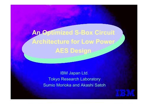
An Optimized S-Box Circuit Architecture for Low Power AES Design
An Optimized S-Box Circuit Architecture for Low Power AES Design
An Optimized S-Box Circuit Architecture for Low Power AES Design

You also want an ePaper? Increase the reach of your titles
YUMPU automatically turns print PDFs into web optimized ePapers that Google loves.
Contents Background <strong>Power</strong> <strong>An</strong>alysis of Conventional S-<strong>Box</strong>es Multi-Stage PPRM S-<strong>Box</strong> <strong>for</strong> <strong>Low</strong>-<strong>Power</strong> H/W Conclusion
Back Ground In 2001, NIST selected Rijndael as the newsymmetric key standard cipher <strong>AES</strong> <strong>AES</strong> H/W will be integrated in various applications <strong>Low</strong>-power feature is important not only in low-endapplications but also in high-end servers A 10-Gbps <strong>AES</strong> H/W chip consumes several Wattsin 0.13-µm CMOS Need <strong>for</strong> power analysis and development of lowpowerarchitectures <strong>for</strong> <strong>AES</strong> H/W
<strong>Power</strong> <strong>An</strong>alysis Method <strong>Power</strong> analysis is based on timing simulation Gate switching including dynamic hazard is evaluated Quite accurate estimation compared with staticanalysisVHDL CodeNet ListWave Formlibrary ieee;use ieee.std_logic;entity XNOR isport (A : in std_logic;B : in std_logic;Y : out std_logic;end XNOR;SynthesisTimingSimulation<strong>Power</strong>Calculationarchitecture RTL of XNOR isbeginsignal T : std_logic;T
<strong>Power</strong> <strong>An</strong>alysis in <strong>AES</strong> H/W 128-bit bus 11-round Loop <strong>Architecture</strong> Table-lookup-based S-<strong>Box</strong> using SOP logic1 %2:1128Data Input75 %10 %1 %15%OthersData RegisterShiftRowsSubBytesMixColumns3:1AddRoundKeyData Output
For <strong>Low</strong>-<strong>Power</strong> <strong>AES</strong> H/W Reducing S-<strong>Box</strong> power is most effective There are various S-<strong>Box</strong> H/W architectures Which architecture is suitable <strong>for</strong> low power ?Objectives Investigate per<strong>for</strong>mance of all conventionalS-<strong>Box</strong>es Develop a low-power S-<strong>Box</strong> architecture
<strong>Power</strong> <strong>An</strong>alysis ofConventional S-<strong>Box</strong>es
S-<strong>Box</strong> Definition Nonlinear byte substitution function Multiplicative Inversion on GF(2 8 ) + affinetrans<strong>for</strong>mation.b =1 0 0 0 1 1 1 11 1 0 0 0 1 1 11 1 1 0 0 0 1 11 1 1 1 0 0 0 11 1 1 1 1 0 0 00 1 1 1 1 1 0 00 0 1 1 1 1 1 00 0 0 1 1 1 1 1a -1 +11000110Affine trans.8x8 XOR matrixInversionComplicated math. logic
S-<strong>Box</strong> <strong>Architecture</strong>sGF inverter + affine Various mathematical techniques can be applied Rather slow Compact implementation S-<strong>Box</strong> and S-<strong>Box</strong> -1 can be mergedDirect mapping Generate black box circuit from a truth table High-speed Rather large S-<strong>Box</strong> and S-<strong>Box</strong> -1 cannot be merged
GF Inverter + Affine Apply hieratical structure of composite field GF(((2 2 ) 2 ) 2 ) Map elements on GF(2 8 ) onto GF(((2 2 ) 2 ) 2 ) by isomorphism Each component is constructed using AND-XOR logicGF(2 8 )isomorphismGF(((2 2 ) 2 ))2inversionGF(((2 2 ))GF((22 )2)GF(2 2 )GF(2)2 2)44x 2λx -144GF(2 8 )isomorphismmergedaffine trans.-122x 2φx -122
Direct Mapping 2-Level Logic SOP (Sum of Products) : (NOT)-AND-OR POS (Product of Sums) : (NOT)-OR-AND PPRM (Positive Polarity Reed-Muller) : AND-XOR8-bit inputSeveralhundredwiresANDmatrixOR / XORmatrix8-bit output
Direct Mapping Selector-Based Logic BDD (Binary Decision Diagram) Twisted BDD will appear at ICCD 2002 in Sep.in0 in1 in2 in3 in4 in5 in6 in7in0 in1 in2 in3 in4 in5 in6 in7out0out001out1out101out72:1MUXBDDout7TwistedBDD
<strong>Power</strong> vs. Gate Count Smaller circuits do not always consume less power400<strong>Power</strong> (uW)350300250200150100500.13-µm 1.5-V CMOS @ 10 MHzNominal conditionsBDDPPRMTwistedBDDCompositePOSField SOP TableLookup00 0.5 1 1.5 2 2.5 3Gate Count (Kgate)
<strong>An</strong>alysis <strong>Power</strong> consumption of S-<strong>Box</strong> is greatlyinfluenced by the number of dynamic hazardsCaused by Differences of signal arrival times at each gate Propagation probability of signal transitions
<strong>An</strong>alysisDifferences of signal arrival times at each gate Composite field S-<strong>Box</strong> consumes a lot of powerin spite of having the smallest size It has many crossing and branched signal pathsSwitch many timesx 2λx -1Multiplesignalpaths
<strong>An</strong>alysisPropagation probability of signal transitions <strong>An</strong> XOR gate transfers signal transitions frominput to output with probability 100% For AND, OR gates, the probability is 50% So power <strong>for</strong> SOP is lower than PPRM0XOR1100% Probability0AND0150% Probability1OR10
Multi-Stage PPRM S-<strong>Box</strong><strong>for</strong> <strong>Low</strong>-<strong>Power</strong> H/W
Approach <strong>for</strong> <strong>Low</strong> <strong>Power</strong> S-<strong>Box</strong> Use composite field S-<strong>Box</strong> Reduce gate counts Divide combination logic into multiple stages Reduce probability of signal transitions Adjust the signal timing between each stageusing 2-level logic Reduce the number of dynamic hazardsTransition Probability0.5 1.00.5 1.0 0.5 1.0 0.5 1.0ANDarrayXORarray
Multi-Stage PPRM Composite field S-<strong>Box</strong> is divided into several blocks Each block is designed using PPRM logic suitable <strong>for</strong>GF operations Adjust signal timing by using 2-level (AND-XOR) logic4844x 2λ4x -1444-1+affine84Delay chain8ANDarrayXORarray428 4 AND XOR 4array array4412 ANDarray432XORarray83-stage PPRM
Multi-Stage PPRM PPRM S-<strong>Box</strong>es can be divided many ways (1~6-stages)XOR AND-XOR AND-XOR AND-XOR4844x 2λ-14x -1444+affine8422x 2φx -122AND-XOR AND-XOR AND-XOR
<strong>Power</strong> vs. Gate Count 3-stage PPRM is the most effective architecture Multi-stage SOP is not suitable <strong>for</strong> GF operation8007006000.13-µm 1.5-V CMOS @ 10 MHzNominal conditions2-3-<strong>Power</strong> (uW)50040030020010006-4-3-2-1-stage(normal PPRM)1-stage(normal SOP)0 1 2 3 4 5 6 7Gate Count (Kgate)PPRMSOP
<strong>Power</strong> vs. Gate Count 3-stage PPRM is the most effective architecture Multi-stage SOP is not suitable <strong>for</strong> GF operation<strong>Power</strong> (uW)4003503002502001501005000.13-µm 1.5-V CMOS @ 10 MHzNominal conditionsBDDPPRMCompositePOSField SOP TableLookup3-stage PPRM0 0.5 1 1.5 2 2.5 3Gate Count (Kgate)TwistedBDD1/3 power with 1/2 gates
Conclusion The <strong>AES</strong> S-<strong>Box</strong> (SOP logic) consumes 75% ofthe power Dynamic hazards boost power needs of S-<strong>Box</strong>es A multi-stage PPRM architecture based on acomposite field S-<strong>Box</strong> was developed 3-stage PPRM / SOP : <strong>Power</strong> = 1/3, Size = 1/2 This architecture can be applied to other S-<strong>Box</strong>esdefined over Galois fields