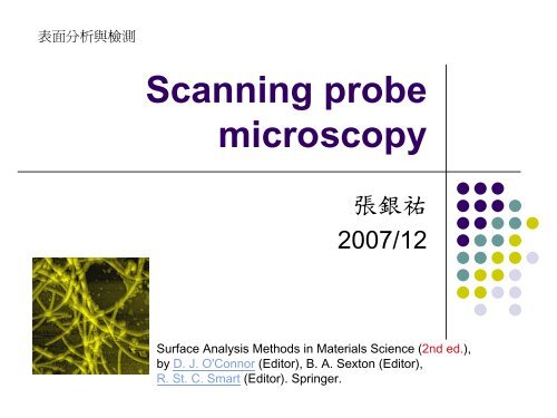
Scanning probe microscopy
Scanning probe microscopy
Scanning probe microscopy
You also want an ePaper? Increase the reach of your titles
YUMPU automatically turns print PDFs into web optimized ePapers that Google loves.
SPM• <strong>Scanning</strong> <strong>probe</strong> <strong>microscopy</strong>covers several relatedtechnologies for imaging andmeasuring surfaces on a finescale, down to the level ofmolecules and groups of atoms.• SPM technologies share theconcept of scanning anextremely sharp tip (3-50 nmradius of curvature) across theobject surface. The tip ismounted on a flexible cantilever,allowing the tip to follow thesurface profile (see Figure).3
Probe Techniques• Atomic Force Microscopy (AFM) measures the interactionforce 相 互 間 作 用 力 between the tip and surface. The tip may bedragged across the surface, or may vibrate as it moves. Theinteraction force will depend on the nature of the sample, the<strong>probe</strong> tip and the distance between them.• <strong>Scanning</strong> Tunneling Microscopy (STM) measures a weakelectrical current 弱 電 流 flowing between tip and sample asthey are held a very distance apart.• Near-Field <strong>Scanning</strong> Optical Microscopy ( 近 場 掃 瞄 光 學 顯 微 鏡NSOM) scans a very small light source very close to thesample. Detection of this light energy forms the image. NSOMcan provide resolution below that of the conventional lightmicroscope.6
AFM• 原 子 力 顯 微 鏡 (atomic force microscope, 簡稱 AFM) 利 用 原 子 之 間 的 凡 德 華 爾 力 作 用 來 呈現 樣 品 的 表 面 特 性 。 利 用 微 懸 臂 間 接 地 感 受 和放 大 原 子 之 間 的 作 用 力 , 從 而 達 到 檢 測 的 目的 。 具 有 原 子 級 的 解 析 度 。 由 於 原 子 力 顯 微 鏡既 可 以 觀 察 導 體 , 也 可 以 觀 察 非 導 體 , 從 而 彌補 了 掃 描 隧 道 顯 微 鏡 的 不 足 。7
AFM 操 作 模 式Mode of Operationcontact modenon-contact mode (tapping mode)intermittent contact modelateral force mode (LFM)magnetic force (MFM)thermal scanningForce of Interactionstrong (repulsive) - constant force orconstant distanceweak (attractive) - vibrating <strong>probe</strong>strong (repulsive) - vibrating <strong>probe</strong>frictional forces exert a torque on thescanning cantileverthe magnetic field of the surface isimagedthe distribution of thermal conductivityis imaged8
AFM 特 點• Sensitive detection– Laser beam deflection• Flexible cantilevers• Sharp tips• High-resolution tip-sample positioning• Force feedbackAFMs can achieve a resolution of 10 pm,and unlike electron microscopes, can image samples in air and under liquids.9
<strong>Scanning</strong>• The <strong>probe</strong> (or the sampleunder a stationary <strong>probe</strong>)generally is moved by apiezoelectric tube.• For atomic force <strong>microscopy</strong>,the sensor is a positionsensitivephotodetector thatrecords the angle of reflectionfrom a laser bean focused onthe top of the cantilever.• Laser beam deflection offersa convenient and sensitivemethod of measuringcantilever deflection.10
AFM cantilevers have highflexibility• Schematic illustration of the meaning of"spring constant" as applied to cantilevers.Visualizing the cantilever as a coil spring,its spring constant k directly affects thedownward force exerted on the sample.• 彈 簧 常 數 (S.C.):~ 0.1 N/m ( 要 小 )• 共 振 頻 率 =(1/2π)(S.C./ 質 量 ) 0.5要 大 要 小 要 小11
AFM cantilevers have highflexibilityelectron-beam-deposited (EBD) tip類 似 DLC 薄 膜(a) (b) (c)R~10nmR~30nmThree common types of AFM tip. (a) normal tip (3 µm tall); (b) supertip;(c) Ultralever (also 3 µm tall).Electron micrographs by Jean-Paul Revel, Caltech.Tips from Park Scientific Instruments; supertip made by Jean-Paul Revel.探 針 尖 端 半 徑 越 小 , 解 析 度 越 高12
Cantilevers and Tips for SPM• Cantilevers are availablewith pyramidal tips orconical tips.• Cantilevers for AFM workare nanofabricated fromsilicon. The cantileversshown at right are stillattached to the originalchip. These cantilevers arefabricated with pyramidaltips of silicon nitride.微 加 工 技 術13
Tube piezoceramics position thetip or sample with high resolution• Piezoelectric ceramics:create a voltage gradient 電 壓差 when forced to expand orcontract• Piezoceramics make itpossible to create threedimensionalpositioning 三 軸 定位 devices of arbitrarily highprecision.管 狀 壓 電 陶 瓷精 確 定 位 機 構14
AFM-- feedback system電 子 回 饋 控 制 系 統• The faster the feedbackloop can correct deviationsof the cantilever deflection,the faster the AFM canacquire images.• Almost all AFMs canmeasure sampletopography in two ways: byrecording the feedbackoutput ("Z") or thecantilever deflection("error"; , “C” see figure).15
Optical lever AFMs can measure thefriction 摩 擦 between tip and sample• While topographic imaging uses the up-and-downdeflection of the cantilever, friction imaging usestorsional deflection 扭 矩 變 化 量 .2.5 x 2.5 nm simultaneous topographic and friction image of highly oriented pyrolytic graphic (HOPG).The bumps represent the topographic atomic corrugation,while the coloring reflects the lateral forces on the tip. The scan direction was right to left.16
大 氣 中 量 測 – 水 氣 污 染 的 影 響• When imaging in air,a layer of watercondensation andother contaminationcovers both the tipand sample, forminga meniscus that pullsthe two together.‧ 測 量 室 環 境 濕 度 與 清 潔 狀 況‧ 試 片 需 清 潔 擦 拭 乾 淨17
Choice of Technique• Contact mode is most useful for hardsurfaces.• Near-contact mode has less tendency todeform a soft surface 不 適 合 用 在 軟 材 上 , butis more sensitive to environmental vibrationsand to variations in the film of moisture thatcoats samples in a normal atmosphere.18
Accuracy and Calibration• The sharpness and stability of the <strong>probe</strong> tipdetermine the area of contact and thereproducibility of imaging.• Obviously, environmental vibrations must becontrolled to a high degree.• Such calibration gratings and calibrationsoftware are commercially available.19
SPM 廠 商DME - Danish Micro Engineering A/SHerlev, DenmarkJPK Instruments AGBerlin, GermanyNT-MDT, Molecular Devices and Toolsfor Nanotechnology,Moscow, RussiaMolecular Imaging Corporation,Phoenix, AZ.Nanosurf AG,Liestal, SwitzerlandNanotec ElectronicaMadrid, SpainNovascan Technologies, Inc.Ames, IAPSIA Corp.Sungnam, KoreaQuantomiXNes-Ziona, IsraelQuesant Instruments,Agoura Hills, CARHK Technology, Inc.,Rochester Hills, MISurface Imaging Systems GmbH,Herzogenrath, GermanyTriple-O Microscopy GmbH,Potsdam, GermanyVeeco Metrology GroupWoodbury, NYOmicron Vacuumphysik GmbH,Taunusstein, GermanyDigital Instruments20
SPM 廠 商 -Digital Instrument( 清 華 大 學 貴 重 儀 器 中 心 )• 廠 牌 及 型 號 :Digitalinstrument NS3a controllerwith D3100 stage• 重 要 規 格 :• Scan size :90μm*90μmZ scale 6μm• 三 軸 誤 差 :≦ ±3%• 主 要 附 件 :• 微 機 械 磨 耗 儀 控 制 單 元• 掃 描 式 電 腦 顯 微 儀 掃 描 頭• 儀 器 性 能 :• AFM 表 面 量 測• 磁 力 影 像 量 測21
SPM 應 用• STM relies on the electrical conductivity ofthe sample, so at least some features on thesample surface must be electricallyconductive to some degree.• AFM is used for studies of non-conductorsand is the technique more commonly used forstudies of macromolecules and biologicalspecimens.22
AFM 應 用Inorganic and SyntheticMaterialsSurfacesNaturalsurfacetopographySurfaceChemistrySiliconwafersDatastoragemediaCeramicsNanostructuresBuckyballsandNanotubesSurfaces ofPolymersDiffractiongratingsIntegratedcircuitsBiological MaterialsPolymersandPolymerMatrixNaturalresins andgumsMuscleproteinsDNAPlant cellwallsBiologicalStructuresBacterialflagellaeAmyloidbetaChromosomesCell andmembranesurfaces23
Buckyballs: Individual C60Molecules on Si(100)Xiaowei Yao, Richard K. Workman, Dong Chen, Dror SaridOptical Sciences Center, University of Arizona, Tucson, AZ 8572124
CD Stamper• Stampers are used to createthe regular - daily use -data/music CDs. Stampersare stainless steel disks withprotrusions that create thepits in a CD.25
PrCe Pellet, 3-D view, 15mmscan• A ceramic pellet ofpraseodymium and ceriumwas scanned. The annealedgrain structure is resolvedeasily, as well as the crystalfacets on individual grains.26
DNA• The reaction between the aminogroup on the DNA and thecarboxyl group on the goldparticle was facilitated using astandard chemical method forjoining carboxyl groups toamino groups. Analysis of theproducts by gel electrophoresisand atomic force <strong>microscopy</strong>(AFM) showed the gold particlesbound to the DNA.27
植 物 :Apple cell wallImage size: 1 x 1 micron28
Bacterial 細 菌 flagellae• True non-contact AFM image ofa tangle of Pseudomonasputida bacterial flagellae. Notethe bright cross-over points areclearly resolved when imagingin non-contact mode. This isbecause the forces acting onthe sample are very much lessthan in contact mode. Imagedon mica and scanned in air.Image size: 2 x 2 microns.29
Low temperature MFM 磁 力 顯 微 鏡 of magnetic fluxvortices in a YBa 2 Cu 3 O 7-x superconductor thin film超 導 體 薄 膜 and the corresponding topographyimaged in non - contact mode SFM at T = 7.6 K.MFMCourtesy of: Dr. H.J. Hug, B. Stiefel, A. Moser, P.J.A. van Schendel, O. Knauff, S. Martinand H.-J. Güntherodt, University of Basel, OMICRON Newsletter Vol. 2, Nr. 2, II/9830
Au(111) polycrystalline filmAu(111) polycrystalline film on a glass substrate - in pure contact mode AFM.31
低 溫 STM– C 60• LT-STM image of individual C 60 molecules onAu(110) at T = 5 K; U = +0.37 V (at thesample), I = 0.17 nA, 2.4 nm x 2.8 nm.• Details of the internal structure becomevisible at low temperatures.2.4 nm x 2.8 nm32
MFM image of nucleated domains "written"with different time periods of tip-samplecontact on a 60 ML Co film1, 2, 4 seconds (lowest row from left)8, 12, 16 seconds (middle row from right)20, 32 and 64 seconds (top row from left).• Bright spots are seen at those placeswhere the MFM tip contacted the surface(white colour denotes repulsiveinteraction); 3 µm x 3 µm. .A. Wadas, M. Dreyer, M. Löhndorf and R. Wiesendanger, University of Hamburg33
A Nanolithography example underprogrammed control of the STMtip34
Blue NickelMedia : Nickel (110)35
Software for <strong>Scanning</strong> ProbeMicroscopy• The <strong>Scanning</strong> Probe ImageProcessor, SPIP An image processing programdesigned with focus on characterization of SPMinstruments and accurate quantification of imagestructures. Other instruments like interferencemicroscopes, profilers and scanning electronmicroscopes are also supported.http://www.nanoscience.com/products/SPIP.html• SPM Calibrator Pro- a system for calibrating scanning <strong>probe</strong> microscopes36
3D Surface View Software• Interactive 3D scientificvisualization with real timerendering.• Aimed for R&D in the fieldof scanning <strong>microscopy</strong>(SPM, AFM, STM, SNOM,NSOM, etc.) as well as 3DLaser Beam measurement.37


