LTC1733 - Monolithic Linear Lithium-Ion Battery Charger with ...
LTC1733 - Monolithic Linear Lithium-Ion Battery Charger with ...
LTC1733 - Monolithic Linear Lithium-Ion Battery Charger with ...

You also want an ePaper? Increase the reach of your titles
YUMPU automatically turns print PDFs into web optimized ePapers that Google loves.
FEATURES<br />
■ Complete <strong>Linear</strong> <strong>Charger</strong> for 1-Cell <strong>Lithium</strong>-<strong>Ion</strong><br />
Batteries<br />
■ Thermal Regulation Maximizes Charging Rate<br />
<strong>with</strong>out Risk of Overheating*<br />
■ No External MOSFET, Sense Resistor or Blocking<br />
Diode Required<br />
■ Up to 1.5A Charge Current<br />
■ Preset Charge Voltage <strong>with</strong> 1% Accuracy<br />
■ Programmable Charge Current <strong>with</strong> 7% Accuracy<br />
■ Programmable Charge Termination Timer<br />
■ Tiny Thermally Enhanced 10-Pin MSOP Package<br />
■ Charge Current Monitor Useful for Gas Gauging*<br />
■ C/10 Charge Current Detection Output<br />
■ Automatic Recharge<br />
■ Thermistor Input for Temperature Qualified Charging<br />
■ AC Present Logic Output<br />
■ 4.1V/4.2V Pin Selectable Output Voltage<br />
APPLICATIO S<br />
U<br />
■ Cellular Telephones<br />
■ Handheld Computers<br />
■ Digital Still Cameras<br />
■ Charging Docks and Cradles<br />
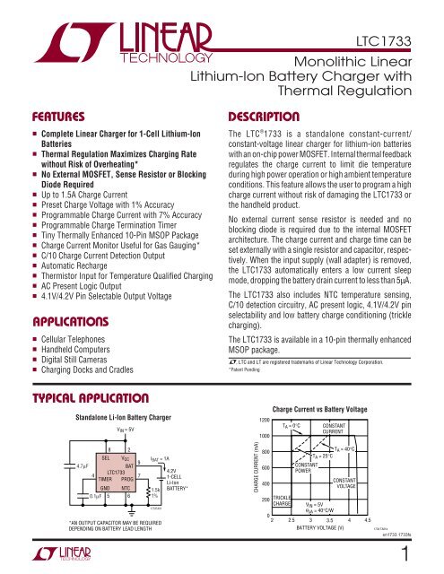
TYPICAL APPLICATIO U<br />
Standalone Li-<strong>Ion</strong> <strong>Battery</strong> <strong>Charger</strong><br />
4.7µF<br />
GND<br />
V IN = 5V<br />
8 2<br />
SEL<br />
VCC<br />
BAT<br />
9<br />
4<br />
<strong>LTC1733</strong><br />
TIMER PROG<br />
7<br />
0.1µF<br />
5<br />
NTC<br />
6<br />
I BAT = 1A<br />
1.5k<br />
1%<br />
1733TA01<br />
*AN OUTPUT CAPACITOR MAY BE REQUIRED<br />
DEPENDING ON BATTERY LEAD LENGTH<br />
4.2V<br />
1-CELL<br />
Li-<strong>Ion</strong><br />
BATTERY*<br />
<strong>LTC1733</strong><br />
<strong>Monolithic</strong> <strong>Linear</strong><br />
<strong>Lithium</strong>-<strong>Ion</strong> <strong>Battery</strong> <strong>Charger</strong> <strong>with</strong><br />
Thermal Regulation<br />
DESCRIPTIO U<br />
The LTC ® 1733 is a standalone constant-current/<br />
constant-voltage linear charger for lithium-ion batteries<br />
<strong>with</strong> an on-chip power MOSFET. Internal thermal feedback<br />
regulates the charge current to limit die temperature<br />
during high power operation or high ambient temperature<br />
conditions. This feature allows the user to program a high<br />
charge current <strong>with</strong>out risk of damaging the <strong>LTC1733</strong> or<br />
the handheld product.<br />
No external current sense resistor is needed and no<br />
blocking diode is required due to the internal MOSFET<br />
architecture. The charge current and charge time can be<br />
set externally <strong>with</strong> a single resistor and capacitor, respectively.<br />
When the input supply (wall adapter) is removed,<br />
the <strong>LTC1733</strong> automatically enters a low current sleep<br />
mode, dropping the battery drain current to less than 5μA.<br />
The <strong>LTC1733</strong> also includes NTC temperature sensing,<br />
C/10 detection circuitry, AC present logic, 4.1V/4.2V pin<br />
selectability and low battery charge conditioning (trickle<br />
charging).<br />
The <strong>LTC1733</strong> is available in a 10-pin thermally enhanced<br />
MSOP package.<br />
, LTC and LT are registered trademarks of <strong>Linear</strong> Technology Corporation.<br />
*Patent Pending<br />
CHARGE CURRENT (mA)<br />
1200<br />
1000<br />
800<br />
600<br />
400<br />
200<br />
0<br />
2<br />
Charge Current vs <strong>Battery</strong> Voltage<br />
T A = 0°C<br />
TRICKLE<br />
CHARGE<br />
CONSTANT<br />
CURRENT<br />
TA = 25°C<br />
CONSTANT<br />
POWER<br />
VIN = 5V<br />
θJA = 40°C/W<br />
T A = 40°C<br />
CONSTANT<br />
VOLTAGE<br />
2.5 3 3.5 4 4.5<br />
BATTERY VOLTAGE (V)<br />
1733 TA01b<br />
sn1733 1733fs<br />
1
<strong>LTC1733</strong><br />
ABSOLUTE AXI U RATI GS<br />
(Note 1)<br />
Input Supply Voltage (VCC) ........................................ 7V<br />
BAT ............................................................................ 7V<br />
NTC, SEL, TIMER, PROG ................ –0.3V to VCC + 0.3V<br />
CHRG, FAULT, ACPR ................................... –0.3V to 7V<br />
BAT Short-Circuit Duration ...........................Continuous<br />
BAT Current (Note 2) .............................................. 1.6A<br />
PROG Current (Note 2) ........................................ 1.6mA<br />
Junction Temperature........................................... 125°C<br />
Operating Temperature Range (Note 3) ...–40°C to 85°C<br />
Storage Temperature Range ................. –65°C to 150°C<br />
Lead Temperature (Soldering, 10 sec).................. 300°C<br />
2<br />
W W W<br />
U<br />
ELECTRICAL CHARACTERISTICS<br />
U U W<br />
PACKAGE/ORDER I FOR ATIO<br />
MSE EXPOSED PAD PACKAGE<br />
10-LEAD PLASTIC MSOP<br />
TJMAX = 125°C, θJA = 40°C/W (Note 4)<br />
EXPOSED PAD IS GROUND.<br />
(MUST BE SOLDERED TO PCB<br />
FOR MAXIMUM HEAT TRANSFER).<br />
ORDER PART<br />
NUMBER<br />
<strong>LTC1733</strong>EMSE<br />
MSE PART MARKING<br />
Consult LTC Marketing for parts specified <strong>with</strong> wider operating temperature ranges.<br />
SYMBOL PARAMETER CONDITIONS MIN TYP MAX UNITS<br />
V CC V CC Supply Voltage ● 4.5 6.5 V<br />
ICC VCC Supply Current <strong>Charger</strong> On; Current Mode; RPROG = 30k (Note 5) ● 1 3 mA<br />
Shutdown Mode; VPROG = 3V ● 0.9 2 mA<br />
VBAT VBAT Regulated Output Voltage SEL = 0V ● 4.059 4.1 4.141 V<br />
SEL = VCC ● 4.158 4.2 4.242 V<br />
IBAT <strong>Battery</strong> Pin Current RPROG = 3k; Current Mode ● 465 500 535 mA<br />
RPROG = 1k; Current Mode 1.395 1.5 1.605 A<br />
Shutdown Mode; VPROG = 3V ±1 ±5 μA<br />
Sleep Mode VCC < VBAT or VCC < (VUV – ΔVUV) ±1 ±5 μA<br />
I TRIKL Trickle Charge Current V BAT < 2V; R PROG = 3k ● 35 50 65 mA<br />
V TRIKL Trickle Charge Trip Threshold V BAT Rising 2.48 V<br />
ΔVTRIKL Trickle Charge Trip Hysteresis 100 mV<br />
V UV V CC Undervoltage Lockout Voltage V CC Rising ● 4.2 4.5 V<br />
ΔVUV VCC Undervoltage Lockout Hysteresis 150 mV<br />
V MSD Manual Shutdown Threshold Voltage PROG Pin Voltage Rising 2.15 V<br />
V MSD-HYS Manual Shutdown Hysteresis Voltage 100 mV<br />
VASD Automatic Shutdown Threshold Voltage (VCC - VBAT) Voltage Falling 30 mV<br />
(VCC - VBAT) Voltage Rising 60 mV<br />
CHRG<br />
VCC<br />
FAULT<br />
TIMER<br />
GND<br />
1<br />
2<br />
3<br />
4<br />
5<br />
TOP VIEW<br />
The ● denotes the specifications which apply over the full operating<br />
temperature range, otherwise specifications are at TA = 25°C. VCC = 5V<br />
10<br />
9<br />
8<br />
7<br />
6<br />
ACPR<br />
BAT<br />
SEL<br />
PROG<br />
NTC<br />
LTLX<br />
sn1733 1733fs
ELECTRICAL CHARACTERISTICS T A = 25°C. V CC = 5V unless otherwise noted.<br />
Note 1: Absolute Maximum Ratings are those values beyond which the life<br />
of a device may be impaired.<br />
Note 2: The Absolute Maximum BAT Current Rating of 1.6A is guaranteed<br />
by design and current density calculations. The Absolute Maximum PROG<br />
Current Rating is guaranteed to be 1/1000 of BAT current rating by design.<br />
Note 3: The <strong>LTC1733</strong>E is guaranteed to meet performance specifications<br />
from 0°C to 70°C. Specifications over the –40°C to 85°C operating<br />
<strong>LTC1733</strong><br />
SYMBOL PARAMETER CONDITIONS MIN TYP MAX UNITS<br />
VPROG PROG Pin Voltage RPROG = 3k, IPROG = 500μA; Current Mode 1.5 V<br />
ICHRG CHRG Pin Weak Pulldown Current VCHRG = 1V 25 μA<br />
V CHRG CHRG Pin Output Low Voltage I CHRG = 5mA 0.35 V<br />
VACPR ACPR Pin Output Low Voltage IACPR = 5mA 0.35 V<br />
VFAULT FAULT Pin Output Low Voltage IFAULT = 5mA 0.35 V<br />
I C/10 End of Charge Indication Current Level R PROG = 3k 35 50 65 mA<br />
tTIMER TIMER Accuracy CTIMER = 0.1μF ±10 %<br />
VRECHRG Recharge <strong>Battery</strong> Voltage Threshold <strong>Battery</strong> Voltage Falling, SEL = 0V 3.9 V<br />
<strong>Battery</strong> Voltage Falling, SEL = 5V 4.0 V<br />
VNTC-HOT NTC Pin Hot Threshold Voltage VNTC Falling 2.5 V<br />
VHOT-HYS NTC Pin Hot Hysteresis Voltage 70 mV<br />
VNTC-COLD NTC Pin Cold Threshold Voltage VNTC Rising 4.375 V<br />
V COLD-HYS NTC Pin Cold Hystersis Voltage 70 mV<br />
V NTC-DIS NTC Pin Disable Threshold Voltage V NTC Rising 100 mV<br />
V DIS-HYS NTC Pin Disable Hystersis Voltage 10 mV<br />
V SEL-IL SEL Pin Threshold Input Low 0.3 V<br />
V SEL-IH SEL Pin Threshold Input High 1 V<br />
TLIM Junction Temperature in<br />
Constant-Temperature Mode<br />
105 °C<br />
RON Power MOSFET “ON” Resistance 375 mΩ<br />
temperature range are assured by design, characterization and correlation<br />
<strong>with</strong> statistical process controls.<br />
Note 4: Failure to solder the exposed backside of the package to the PC<br />
board will result in a thermal resistance much higher than 40°C/W.<br />
Note 5: Supply current includes PROG pin current but does not include<br />
any current delivered to the battery through the BAT pin.<br />
sn1733 1733fs<br />
3
<strong>LTC1733</strong><br />
TYPICAL PERFOR A CE CHARACTERISTICS<br />
V BAT (V)<br />
V PROG (V)<br />
IBAT (mA)<br />
4<br />
4.24<br />
4.22<br />
4.20<br />
4.18<br />
4.16<br />
4.14<br />
4.12<br />
4.10<br />
4.08<br />
UW<br />
<strong>Battery</strong> Regulation Voltage vs<br />
<strong>Battery</strong> Charge Current<br />
VSEL = 5V<br />
V SEL = 0V<br />
4.06<br />
0 100 200 300 400 500 600 700 800 900 1000<br />
1.6<br />
1.4<br />
1.2<br />
1.0<br />
0.8<br />
0.6<br />
0.4<br />
0.2<br />
1100<br />
1000<br />
900<br />
800<br />
700<br />
600<br />
500<br />
I BAT (mA)<br />
VCC = 5V<br />
TA = 25°C<br />
RPROG = 1.5k<br />
PROG Pin Voltage vs Charge<br />
Current<br />
VCC = 5V<br />
TA = 25°C<br />
R PROG = 1.5k<br />
VSEL = 5V<br />
1733 G01<br />
0<br />
0 100 200 300 400 500 600 700 800 900 1000<br />
CHARGE CURRENT (mA)<br />
400<br />
4.0<br />
Charge Current vs V CC<br />
RPROG = 1.5k<br />
R PROG = 3k<br />
1733 G04<br />
VBAT = 3.5V<br />
TA = 25°C<br />
V SEL = V CC<br />
4.5 5.0 5.5<br />
VCC (V)<br />
6.0 6.5 7.0<br />
1733 G07<br />
VBAT (V)<br />
I BAT (mA)<br />
IBAT (mA)<br />
4.24<br />
4.22<br />
4.20<br />
4.18<br />
4.16<br />
4.14<br />
4.12<br />
4.10<br />
4.08<br />
<strong>Battery</strong> Regulation Voltage vs<br />
Temperature<br />
V CC = 5V<br />
I BAT = 10mA<br />
R PROG = 1.5k<br />
VSEL = 5V<br />
V SEL = 0V<br />
4.06<br />
–50 –25 0 25 50 75 100 125<br />
TEMPERATURE(°C)<br />
1100<br />
1000<br />
900<br />
800<br />
700<br />
600<br />
500<br />
400<br />
300<br />
200<br />
100<br />
0<br />
0<br />
1000<br />
900<br />
800<br />
700<br />
600<br />
500<br />
400<br />
V CC = 5V<br />
TA = 25°C<br />
RPROG = 1.5k<br />
VSEL = 5V<br />
1733 G02<br />
0.5 1.0 1.5 2.0 2.5 3.0 3.5 4.0 4.5<br />
VBAT (V)<br />
1733 G05<br />
300<br />
200<br />
100<br />
0<br />
VCC = 5V<br />
VBAT = 3.5V<br />
RPROG = 1.5k<br />
VSEL = 5V<br />
–50 –25 0 25 50 75 100<br />
TEMPERATURE (°C)<br />
1733 G08<br />
VBAT (V)<br />
IBAT (mA)<br />
4.24<br />
4.22<br />
4.20<br />
4.18<br />
4.16<br />
4.14<br />
4.12<br />
4.10<br />
4.08<br />
<strong>Battery</strong> Regulation Voltage vs VCC<br />
T A = 25°C<br />
IBAT = 10mA<br />
RPROG = 1.5k<br />
V SEL = V CC<br />
V SEL = 0V<br />
4.06<br />
4.0 4.5 5.0 5.5<br />
VCC (V)<br />
6.0 6.5 7.0<br />
Charge Current vs <strong>Battery</strong> Voltage Charge Current vs Input Voltage<br />
Charge Current vs Temperature<br />
<strong>with</strong> Thermal Regulation<br />
THERMAL CONTROL<br />
LOOP IN OPERATION<br />
I BAT (mA)<br />
1100<br />
1000<br />
900<br />
800<br />
700<br />
600<br />
500<br />
400<br />
300<br />
200<br />
100<br />
0<br />
4.0<br />
Charge Current vs Temperature<br />
1733 G03<br />
VBAT = 4.1V<br />
TA = 25°C<br />
RPROG = 1.5k<br />
VSEL = 5V<br />
4.5 5.0 5.5<br />
VCC (V)<br />
6.0 6.5 7.0<br />
1733 G06<br />
535<br />
530<br />
525<br />
520<br />
515<br />
510<br />
505<br />
500<br />
495<br />
490<br />
485<br />
480<br />
475<br />
470<br />
VCC = 5V<br />
VBAT = 4V<br />
RPROG = 3k<br />
VSEL = 5V<br />
465<br />
–50 –25 0 25 50 75 100<br />
TEMPERATURE (°C)<br />
1733 G09<br />
sn1733 1733fs
TYPICAL PERFOR A CE CHARACTERISTICS<br />
VPROG (V)<br />
IBAT (% OF PROGRAMMED CURRENT)<br />
1.515<br />
1.510<br />
1.505<br />
1.500<br />
1.495<br />
1.490<br />
Trickle Charge Current vs V CC<br />
UW<br />
T A = 25°C<br />
VBAT = 3.5V<br />
RPROG = 3k<br />
VSEL = 5V<br />
1.485<br />
4.0 4.5 5.0 5.5<br />
VCC (V)<br />
6.0 6.5 7.0<br />
13<br />
12<br />
11<br />
10<br />
9<br />
8<br />
PROG Pin Voltage vs V CC<br />
Constant Current Mode<br />
V CC (V)<br />
1733 G10<br />
T A = 25°C<br />
VBAT = 2V<br />
RPROG = 1.5k<br />
VSEL = 5V<br />
7<br />
4.0 4.5 5.0 5.5 6.0 6.5 7.0<br />
1733 G13<br />
VPROG (V)<br />
t TIMER (%)<br />
1.515<br />
1.510<br />
1.505<br />
1.500<br />
1.495<br />
1.490<br />
PROG Pin Voltage vs Temperature<br />
Constant Current Mode<br />
1.485<br />
–50 –25 0 25 50 75 100<br />
TEMPERATURE (°C)<br />
TEMPERATURE(°C)<br />
V CC = 5V<br />
V BAT = 4V<br />
RPROG = 3k<br />
VSEL = 5V<br />
1733 G11<br />
105<br />
104<br />
103<br />
102<br />
101<br />
100<br />
99<br />
98<br />
97<br />
96<br />
95<br />
VCC = 5V<br />
IBAT = 0mA<br />
VSEL = 5V<br />
CTIMER = 0.1µF<br />
–50 –25 0 25 50 75 100 125<br />
1733 G14<br />
I BAT (mA)<br />
tTIMER (%)<br />
130<br />
120<br />
110<br />
100<br />
90<br />
80<br />
Trickle Charge Current vs<br />
Temperature<br />
<strong>LTC1733</strong><br />
70<br />
–50 –25 0 25 50 75 100<br />
TEMPERATURE (°C)<br />
Timer Accuracy vs Temperature Timer Accuracy vs VCC<br />
V CC = 5V<br />
VBAT = 2V<br />
RPROG = 1.5k<br />
VSEL = 5V<br />
1733 G12<br />
105<br />
104<br />
103<br />
102<br />
101<br />
100<br />
99<br />
98<br />
97<br />
96<br />
TA = 25°C<br />
IBAT = 0mA<br />
VSEL = 5V<br />
CTIMER = 0.1µF<br />
95<br />
4.0 4.5 5.0 5.5 6.0 6.5 7.0<br />
V CC (V)<br />
1733 G15<br />
sn1733 1733fs<br />
5
<strong>LTC1733</strong><br />
PI FU CTIO S<br />
6<br />
U U U<br />
CHRG: Open-Drain Charge Status Output. When the<br />
battery is being charged, the CHRG pin is pulled low by an<br />
internal N-channel MOSFET. When the charge current<br />
drops to 10% of the full-scale current, the N-channel<br />
MOSFET latches off and a 25μA current source is connected<br />
from the CHRG pin to ground. The C/10 latch can<br />
be cleared by momentarily pulling the PROG pin above the<br />
2.15V shutdown threshold, or by toggling V CC. When the<br />
timer runs out or the input supply is removed, the current<br />
source is disconnected and the CHRG pin is forced to a<br />
high impedance state.<br />
V CC: Positive Input Supply Voltage. When V CC is <strong>with</strong>in<br />
30mV of VBAT or less than the undervoltage lockout<br />
threshold, the <strong>LTC1733</strong> enters sleep mode, dropping I BAT<br />
to less than 5μA. V CC can range from 4.5V to 6.5V. Bypass<br />
this pin <strong>with</strong> at least a 4.7μF ceramic capacitor to ground.<br />
FAULT: Open-Drain Fault Status Output. The FAULT opendrain<br />
logic signal indicates that the charger has timed out<br />
under trickle charge conditions (1/4 of total time period) or<br />
the NTC comparator is indicating an out-of-range battery<br />
temperature condition. When VBAT is less that 2.48V,<br />
trickle charging activates whereby the charge current<br />
drops to one tenth of its programmed value and the timer<br />
period is reduced by a factor of four. When one fourth of<br />
the timing period has elapsed, if VBAT is still less than<br />
2.48V, trickle charging stops and the FAULT pin latches to<br />
ground. The fault can be cleared by toggling VCC, momentarily<br />
pulling the PROG pin above the 2.15V shutdown<br />
threshold, or pulling the BAT pin above 2.48V. If the NTC<br />
comparator is indicating an out-of-range battery temperature<br />
condition, then the FAULT pin will pull to ground until<br />
the temperature returns to the acceptable range.<br />
TIMER: Timer Capacitor. The timer period is set by placing<br />
a capacitor, CTIMER, to ground. The timer period is:<br />
Time (Hours) = (CTIMER • 3 hr)/(0.1μF)<br />
Short the TIMER pin to ground to disable the internal timer<br />
function.<br />
GND: Ground. Connect exposed back package to ground.<br />
NTC: Input to the NTC (Negative Temperature Coefficient)<br />
Thermistor Temperature Monitoring Circuit. With an external<br />
10kΩ NTC thermistor to ground and a 1% resistor<br />
to VCC, this pin can sense the temperature of the battery<br />
pack and stop charging when it is out of range. When the<br />
voltage at this pin drops below (0.5)•(VCC) at hot temperatures<br />
or rises above (0.875)•(VCC) at cold, charging is<br />
suspended and the internal timer is frozen. The CHRG pin<br />
output status is not affected in this hold state. The FAULT<br />
pin is pulled to ground, but not latched. When the temperature<br />
returns to an acceptable range, charging will resume<br />
and the FAULT pin is released. The NTC feature can be<br />
disabled by grounding the NTC pin.<br />
PROG: Charge Current Program, Shutdown Input and<br />
Charge Current Monitor Pin. The charge current is programmed<br />
by connecting a resistor, RPROG to ground.<br />
When in constant-current mode, the <strong>LTC1733</strong> servos the<br />
PROG pin voltage to 1.5V. In all modes the voltage on the<br />
PROG pin can be used to measure the charge current as<br />
follows:<br />
ICHG = (VPROG/RPROG) • 1000.<br />
The IC can be forced into shutdown by pulling the PROG<br />
pin above the 2.15V shutdown threshold voltage (note: it<br />
will not be pulled up when allowed to float).<br />
SEL: 4.1V/4.2V <strong>Battery</strong> Selection Input. Grounding this<br />
pin sets the battery float voltage to 4.1V, while connecting<br />
to VCC sets the voltage to 4.2V.<br />
BAT: Charge Current Output. A bypass capacitor of at least<br />
1μF <strong>with</strong> a 1Ω series resistor is required to minimize ripple<br />
voltage when the battery is not present. A precision<br />
internal resistor divider sets the final float potential on this<br />
pin. The internal resistor divider is disconnected in sleep<br />
and shutdown modes.<br />
ACPR: Open-Drain Power Supply Status Output. When<br />
V CC is greater than the undervoltage lockout threshold<br />
and at least 30mV above VBAT, the ACPR pin will pull to<br />
ground. Otherwise, the pin is forced to a high impedance<br />
state.<br />
sn1733 1733fs
SI PLIFIED<br />
W<br />
NTC<br />
CHRG<br />
ACPR 10<br />
FAULT<br />
6<br />
1<br />
3<br />
BLOCK DIAGRA<br />
105°C<br />
T DIE<br />
25µA<br />
HOT COLD DISABLE<br />
STOP<br />
FAULT<br />
COUNTER<br />
OSCILLATOR<br />
–<br />
+<br />
C/10<br />
ACPR<br />
TA<br />
NTC<br />
LOGIC<br />
C TIMER<br />
SHDN<br />
CHARGE<br />
W<br />
Figure 1.<br />
2.485V<br />
+<br />
–<br />
+<br />
–<br />
+<br />
–<br />
+<br />
–<br />
C3<br />
CA<br />
D1<br />
D2<br />
D3<br />
C1<br />
C2<br />
–<br />
+<br />
M2<br />
×1<br />
MP<br />
– +<br />
2.485V TO BAT<br />
4<br />
TIMER<br />
7<br />
PROG<br />
5<br />
GND<br />
2.15V<br />
1.5V<br />
0.15V<br />
RPROG<br />
R4<br />
R5<br />
R6<br />
R7<br />
MA<br />
REF<br />
V CC<br />
2<br />
30µA<br />
VA<br />
M1<br />
×1000<br />
R1<br />
R2<br />
R3<br />
<strong>LTC1733</strong><br />
2.5µA<br />
9<br />
8<br />
1733 F01<br />
BAT<br />
SEL<br />
sn1733 1733fs<br />
7
<strong>LTC1733</strong><br />
OPERATIO U<br />
The <strong>LTC1733</strong> is a linear battery charger designed primarily<br />
for charging single cell lithium-ion batteries. Featuring an<br />
internal P-channel power MOSFET, the charger uses a<br />
constant-current/constant-voltage charge algorithm <strong>with</strong><br />
programmable current and a programmable timer for<br />
charge termination. Charge current can be programmed<br />
up to 1.5A <strong>with</strong> a final float voltage accuracy of ±1%. No<br />
blocking diode or sense resistor is required thus dropping<br />
the external component count to three for the basic<br />
charger circuit. The CHRG, ACPR, and FAULT open-drain<br />
status outputs provide information regarding the status of<br />
the <strong>LTC1733</strong> at all times. An NTC thermistor input<br />
provides the option of charge qualification using battery<br />
temperature.<br />
An internal thermal limit reduces the programmed charge<br />
current if the die temperature attempts to rise above a<br />
preset value of approximately 105°C. This feature protects<br />
the <strong>LTC1733</strong> from excessive temperature, and allows the<br />
user to push the limits of the power handling capability of<br />
a given circuit board <strong>with</strong>out risk of damaging the <strong>LTC1733</strong><br />
or the external components. Another benefit of the <strong>LTC1733</strong><br />
thermal limit is that charge current can be set according to<br />
typical, not worst-case, ambient temperatures for a given<br />
application <strong>with</strong> the assurance that the charger will automatically<br />
reduce the current in worst-case conditions.<br />
The charge cycle begins when the voltage at the VCC pin<br />
rises above the UVLO level and a program resistor is<br />
connected from the PROG pin to ground. At the beginning<br />
of the charge cycle, if the battery voltage is below 2.48V,<br />
the charger goes into trickle charge mode to bring the cell<br />
voltage up to a safe level for charging. The charger goes<br />
8<br />
into the fast charge constant-current mode once the<br />
voltage on the BAT pin rises above 2.48V. In constantcurrent<br />
mode, the charge current is set by RPROG.<br />
When the battery approaches the final float voltage, the<br />
charge current begins to decrease as the <strong>LTC1733</strong> switches<br />
to constant-voltage mode. When the current drops to 10%<br />
of the full-scale charge current, an internal comparator<br />
latches off the MOSFET at the CHRG pin and connects a<br />
weak current source to ground to indicate a near end-ofcharge<br />
(C/10) condition. The C/10 latch can be cleared by<br />
momentarily pulling the PROG pin above the 2.15V<br />
shutdown threshold, or momentarily removing and reapplying<br />
VCC. An external capacitor on the TIMER pin sets the total<br />
charge time. When this time elapses the charge cycle<br />
terminates and the CHRG pin assumes a high impedance<br />
state. To restart the charge cycle, simply remove the input<br />
voltage and reapply it, or force the PROG pin above the<br />
2.15V shutdown threshold (note: simply floating the PROG<br />
pin will not restart the charging cycle.<br />
For lithium-ion and similar batteries that require accurate<br />
final float potential, the internal reference, voltage amplifier<br />
and the resistor divider provide regulation <strong>with</strong> ±1%<br />
(max) accuracy.<br />
When the input voltage is not present, the charger goes<br />
into a sleep mode, dropping battery drain current, IBAT, to<br />
less than 5μA. This greatly reduces the current drain on the<br />
battery and increases the standby time. The charger can be<br />
shut down (ICC = 0.9mA) by forcing the PROG pin above<br />
2.15V.<br />
sn1733 1733fs
APPLICATIO S I FOR ATIO<br />
U W U<br />
U<br />
Undervoltage Lockout (UVLO)<br />
An internal undervoltage lockout circuit monitors the input<br />
voltage and keeps the charger in shutdown mode until VCC<br />
rises above the undervoltage lockout threshold. The UVLO<br />
circuit has a built-in hysteresis of 150mV. Furthermore, to<br />
protect against reverse current in the power MOSFET, the<br />
UVLO circuit keeps the charger in shutdown mode if VCC falls to <strong>with</strong>in 30mV of the battery voltage. If the UVLO<br />
comparator is tripped, the charger will not come out of<br />
shutdown until VCC rises 60mV above the battery voltage.<br />
Trickle Charge and Defective <strong>Battery</strong> Detection<br />
At the beginning of a charge cycle, if the battery voltage is<br />
low (below 2.48V) the charger goes into trickle charge<br />
reducing the charge current to 10% of the full-scale<br />
current. If the low battery voltage persists for one quarter<br />
of the total charge time, the battery is assumed to be<br />
defective, the charge cycle is terminated, the CHRG pin<br />
output assumes a high impedance state, and the FAULT<br />
pin latches low. The fault can be cleared by toggling VCC,<br />
temporarily forcing the PROG pin above 2.15V, or temporarily<br />
forcing the BAT pin voltage above 2.48V.<br />
Shutdown<br />
The <strong>LTC1733</strong> can be shutdown (ICC = 0.9mA) by pulling<br />
the PROG pin above the 2.15V shutdown threshold voltage.<br />
In shutdown the internal linear regulator is turned off,<br />
and the internal timer is reset.<br />
Recharge<br />
The <strong>LTC1733</strong> has the ability to recharge a battery<br />
assuming that the battery voltage has been charged above<br />
4.05V (SEL = 5V) or 3.95V (SEL = 0V). Once above these<br />
thresholds, a new charge cycle will begin if the battery<br />
voltage drops below 4V (SEL = 5V) or 3.9V (SEL = 0V) due<br />
to either a load on the battery or self-discharge. The<br />
recharge circuit integrates the BAT pin voltage for a few<br />
milliseconds to prevent a transient from restarting the<br />
charge cycle.<br />
If the battery voltage remains below 2.48V during trickle<br />
charge for 1/4 of the programmed time, the battery may be<br />
defective and the charge cycle will end. In addition, the<br />
<strong>LTC1733</strong><br />
recharge comparator is disabled and a new charge cycle<br />
will not begin unless the input voltage is toggled, the PROG<br />
pin is pulled above the 2.15V shutdown threshold, or the<br />
BAT pin is pulled above the 2.48V trickle charge threshold.<br />
Programming Charge Current<br />
The formula for the battery charge current (see Figure 1)<br />
is:<br />
ICHG = (IPROG) • 1000<br />
= (1.5V / RPROG) • 1000 or<br />
RPROG = 1500/ICHG<br />
where RPROG is the total resistance from the PROG pin to<br />
ground. Under trickle charge conditions, this current is<br />
reduced to 10% of the full-scale value.<br />
For example, if 500mA charge current is required,<br />
calculate:<br />
RPROG = 1500/0.5A = 3kΩ<br />
For best stability over temperature and time, 1% metalfilm<br />
resistors are recommended.<br />
If the charger is in constant-temperature or constantvoltage<br />
mode, the battery current can be monitored by<br />
measuring the PROG pin voltage as follows:<br />
ICHG = (VPROG / RPROG) • 1000<br />
Programming the Timer<br />
The programmable timer is used to terminate the charge<br />
cycle. The timer duration is programmed by an external<br />
capacitor at the TIMER pin. The total charge time is:<br />
Time (Hours) = (3 Hours) • (CTIMER / 0.1μF) or<br />
CTIMER = 0.1μF • Time (Hours)/3 (Hours)<br />
The timer starts when an input voltage greater than the<br />
undervoltage lockout threshold level is applied and the<br />
program resistor is connected to ground. After a time-out<br />
occurs, the charge current stops, and the CHRG output<br />
assumes a high impedance state to indicate that the<br />
charging has stopped. Connecting the TIMER pin to ground<br />
disables the timer function.<br />
sn1733 1733fs<br />
9
<strong>LTC1733</strong><br />
APPLICATIO S I FOR ATIO<br />
Open-Drain Status Outputs<br />
The <strong>LTC1733</strong> has three open-drain status outputs: ACPR,<br />
CHRG and FAULT. The ACPR pin pulls low when an input<br />
voltage greater than the undervoltage lockout threshold is<br />
applied and goes high impedance when power (VIN < VUV)<br />
is removed. CHRG and FAULT work together to indicate<br />
the status of the charge cycle. Table 1 describes the status<br />
of the charge cycle based on the CHRG and FAULT<br />
outputs.<br />
Table 1.<br />
FAULT CHRG Description<br />
High Low Charge cycle has started, C/10 has not been<br />
reached and charging is proceeding normally.<br />
Low Low Charge cycle has started, C/10 has not been<br />
reached, but the charge current and timer<br />
have been paused due to an NTC out-oftemperature<br />
condition.<br />
High 25μA C/10 has been reached and charging is<br />
pulldown proceeding normally.<br />
Low 25μA C/10 has been reached but the charge current<br />
pulldown and timer have paused due to an<br />
NTC out-of-temperature condition.<br />
High High Normal timeout (charging has terminated).<br />
Low High If FAULT goes low and CHRG goes high<br />
impedance simultaneously, then the <strong>LTC1733</strong><br />
has timed out due to a bad cell (VBAT
APPLICATIO S I FOR ATIO<br />
resistance of the NTC thermistor rises. The <strong>LTC1733</strong> is<br />
designed to go into hold mode when the value of the NTC<br />
thermistor increases to seven times the value of RHOT. For<br />
a Vishay NTHS0603N02N1002J thermistor, this value is<br />
28.2k which corresponds to approximately 0°C. The hot<br />
and cold comparators each have approximately 2°C of<br />
hysteresis to prevent oscillation about the trip point. The<br />
NTC function can be disabled by grounding the NTC pin.<br />
RHOT<br />
1%<br />
R NTC<br />
10k<br />
VCC<br />
NTC<br />
7/8 V CC<br />
1/2 V CC<br />
3/160 V CC<br />
<strong>LTC1733</strong><br />
U W U U<br />
–<br />
+<br />
+<br />
–<br />
+<br />
–<br />
Figure 3.<br />
TOO COLD<br />
TOO HOT<br />
DISABLE NTC<br />
1733 F03<br />
Thermistors<br />
The <strong>LTC1733</strong> NTC trip points were designed to work <strong>with</strong><br />
thermistors whose resistance-temperature characteristics<br />
follow Vishay Dale’s “R-T Curve 2”. The Vishay<br />
NTHS0603N02N1002J is an example of such a thermistor.<br />
However, Vishay Dale has many thermistor products<br />
that follow the “R-T Curve 2” characteristic in a variety<br />
of sizes. Futhermore, any thermistor whose ratio of RCOLD to RHOT is about 7.0 will also work (Vishay Dale R-T Curve<br />
2 shows a ratio of RCOLD to RHOT of 2.816/0.4086 = 6.9).<br />
NTC Layout Considerations<br />
It is important that the NTC thermistor not be in close<br />
thermal contact <strong>with</strong> the <strong>LTC1733</strong>. Because the <strong>LTC1733</strong><br />
package can reach temperatures in excess of the 50°C trip<br />
point, the NTC function can cause a hysteretic oscillation<br />
which turns the charge current on and off according to the<br />
<strong>LTC1733</strong><br />
package temperature rather than the battery temperature.<br />
This problem can be eliminated by thermally coupling the<br />
NTC thermistor to the battery and not to the <strong>LTC1733</strong>.<br />
Furthermore, it is essential that the VCC connection to<br />
RHOT is made according to standard Kelvin sense techniques.<br />
Since VCC is a high current path into the <strong>LTC1733</strong>,<br />
it is essential to minimize voltage drops between the VCC input pin and the top of RHOT.<br />
NTC Trip Point Errors<br />
When a 1% resistor is used for RHOT, the major error in<br />
the 50°C trip point is determined by the tolerance of the<br />
NTC thermistor. A typical 10k NTC thermistor has a ±10%<br />
tolerance. By looking up the temperature coefficient of the<br />
thermistor at 50°C, the tolerance error can be calculated<br />
in degrees centigrade. Consider the Vishay<br />
NTHS0603N02N1002J thermistor which has a temperature<br />
coefficient of –3.3%/°C at 50°C. Dividing the tolerance<br />
by the temperature coefficient, ±10%/(–3.3%/°C) =<br />
±3°C, gives the temperature error of the hot trip point.<br />
The cold trip point is a little more complicated because its<br />
error depends on the tolerance of the NTC thermistor and<br />
the degree to which the ratio of its value at 0°C and its value<br />
at 50°C varies from 7 to 1. Therefore, the cold trip point<br />
error can be calculated using the tolerance, TOL, the<br />
temperature coefficient of the thermistor at 0°C, TC<br />
(in %/°C), the value of the thermistor at 0°C, RCOLD, and<br />
the value of the thermistor at 50°C, RHOT. The formula is:<br />
⎛ 1+<br />
TOL RCOLD<br />
⎞<br />
⎜ • – 1⎟ •100<br />
Temperature Error (°C) = ⎝ 7 RHOT<br />
⎠<br />
TC<br />
For example, the Vishay NTHS0603N02N1002J thermistor<br />
<strong>with</strong> a tolerance of ±10%, TC of –4.5%/°C, and R COLD/<br />
RHOT of 6.89, has a cold trip point error of:<br />
⎛ 1± 0. 10 ⎞<br />
⎜ • 6. 89 – 1⎟ •100<br />
Temperature Error (°C) = ⎝ 7 ⎠<br />
– 45 .<br />
= –1.8°C, +2.5°C<br />
sn1733 1733fs<br />
11
<strong>LTC1733</strong><br />
APPLICATIO S I FOR ATIO<br />
If a thermistor <strong>with</strong> a tolerance less than ±10% is used, the<br />
trip point errors begin to depend on errors other than<br />
thermistor tolerance including the input offset voltage of<br />
the internal comparators of the <strong>LTC1733</strong> and the effects of<br />
internal voltage drops due to high charging currents.<br />
Constant-Current/Constant-Voltage/<br />
Constant-Temperature<br />
The <strong>LTC1733</strong> uses a unique architecture to charge a<br />
battery in a constant-current, constant-voltage, constanttemperature<br />
fashion. Figure 1 shows a simplified block<br />
diagram of the <strong>LTC1733</strong>. Three of the amplifier feedback<br />
loops shown control the constant-current, CA, constantvoltage,<br />
VA, and constant-temperature, TA modes. A<br />
fourth amplifier feedback loop, MA, is used to increase the<br />
output impedance of the current source pair, M1 and M2<br />
(note that M1 is the internal P-channel power MOSFET). It<br />
ensures that the drain current of M1 is exactly 1000 times<br />
greater than the drain current of M2.<br />
Amplifiers CA, TA, and VA are used in three separate<br />
feedback loops to force the charger into constant-current,<br />
temperature, or voltage mode, respectively. Diodes, D1,<br />
D2, and D3 provide priority to whichever loop is trying to<br />
reduce the charging current the most. The outputs of the<br />
other two amplifiers saturate low which effectively removes<br />
their loops from the system. When in constantcurrent<br />
mode, CA servos the voltage at the PROG pin to be<br />
precisely 1.50V (or 0.15V when in trickle-charge mode).<br />
TA limits the die temperature to approximately 105°C<br />
when in constant-temperature mode and the PROG pin<br />
voltage gives an indication of the charge current as discussed<br />
in “Programming Charge Current” . VA servos its<br />
inverting input to precisely 2.485V when in constantvoltage<br />
mode and the internal resistor divider made up of<br />
R1 and R2 ensures that the battery voltage is maintained<br />
at either 4.1V or 4.2V. Again, the PROG pin voltage gives<br />
an indication of the charge current.<br />
In typical operation, the charge cycle begins in constantcurrent<br />
mode <strong>with</strong> the current delivered to the battery<br />
equal to 1500V/RPROG. If the power dissipation of the<br />
<strong>LTC1733</strong> results in the junction temperature approaching<br />
105°C, the amplifier (TA) will begin decreasing the charge<br />
current to limit the die temperature to approximately<br />
12<br />
U W U<br />
U<br />
105°C. As the battery voltage rises, the <strong>LTC1733</strong> either<br />
returns to constant-current mode or it enters constantvoltage<br />
mode straight from constant-temperature mode.<br />
Regardless of mode, the voltage at the PROG pin is<br />
proportional to the current being delivered to the battery.<br />
Power Dissipation<br />
The conditions that cause the <strong>LTC1733</strong> to reduce charge<br />
current due to the thermal protection feedback can be<br />
approximated by considering the power dissipated in the<br />
IC. For high charge currents, the <strong>LTC1733</strong> power dissipation<br />
is approximately:<br />
PD = (VCC – VBAT) • IBAT where PD is the power dissipated, VCC is the input supply<br />
voltage, VBAT is the battery voltage, and IBAT is the battery<br />
charge current. It is not necessary to perform any worstcase<br />
power dissipation scenarios because the <strong>LTC1733</strong><br />
will automatically reduce the charge current to maintain<br />
the die temperature at approximately 105°C. However, the<br />
approximate ambient temperature at which the thermal<br />
feedback begins to protect the IC is:<br />
TA = 105°C – P Dθ JA<br />
T A = 105°C – (V CC – V BAT) • I BAT • θ JA<br />
Example: Consider an <strong>LTC1733</strong> operating from a 5V wall<br />
adapter providing 1.2A to a 3.75V Li-<strong>Ion</strong> battery. The<br />
ambient temperature above which the <strong>LTC1733</strong> will begin<br />
to reduce the 1.2A charge current is approximately:<br />
TA = 105°C – (5V – 3.75V) • 1.2A • 40°C/W<br />
TA = 105°C – 1.5W • 40°C/W = 105°C – 60°C = 45°C<br />
The <strong>LTC1733</strong> can be used above 45°C, but the charge<br />
current will be reduced below 1.2A. The approximate<br />
charge current at a given ambient temperature can be<br />
approximated by:<br />
I<br />
BAT<br />
105 ° C – TA<br />
=<br />
( V – V )•θ<br />
CC BAT JA<br />
Consider the above example <strong>with</strong> an ambient temperature<br />
of 55°C. The charge current will be reduced to approximately:<br />
sn1733 1733fs
APPLICATIO S I FOR ATIO<br />
U W U U<br />
105° C – 55°<br />
C 50°<br />
C<br />
IBAT<br />
=<br />
= = 1A<br />
( 5V– 3. 75V)• 40°<br />
C / W 50°<br />
C / A<br />
Furthermore, the voltage at the PROG pin will change<br />
proportionally <strong>with</strong> the charge current as discussed in the<br />
Programming Charge Current section.<br />
It is important to remember that <strong>LTC1733</strong> applications do<br />
not need to be designed for worst-case thermal conditions<br />
since the IC will automatically reduce power dissipation<br />
when the junction temperature reaches approximately<br />
105°C. See Design Note 283 for additional information.<br />
Board Layout Considerations<br />
In order to be able to deliver maximum charge current<br />
under all conditions, it is critical that the exposed pad on<br />
the backside of the <strong>LTC1733</strong> package is soldered to the<br />
board. Correctly soldered to a 2500mm2 double-sided<br />
1oz. copper board the <strong>LTC1733</strong> has a thermal resistance<br />
of approximately 40°C/W. Failure to make thermal contact<br />
between the exposed pad on the backside of the package<br />
and the copper board will result in thermal resistances far<br />
greater than 40°C/W. As an example, a correctly soldered<br />
<strong>LTC1733</strong> can deliver over 1250mA to a battery from a 5V<br />
supply at room temperature. Without a backside thermal<br />
connection, this number could drop to less than 500mA.<br />
VCC Bypass Capacitor<br />
Many types of capacitors can be used for input bypassing.<br />
However, caution must be exercised when using multilayer<br />
ceramic capacitors. Because of the self resonant and<br />
high Q characteristics of some types of ceramic capacitors,<br />
high voltage transients can be generated under some<br />
start-up conditions, such as connecting the charger input<br />
to a hot power source. For more information refer to<br />
Application Note 88.<br />
<strong>LTC1733</strong><br />
Stability<br />
The constant-voltage mode feedback loop is stable<br />
<strong>with</strong>out any compensation when a battery is connected.<br />
However, a 1μF capacitor <strong>with</strong> a 1Ω series resistor to GND<br />
is recommended at the BAT pin to keep ripple voltage low<br />
when the battery is disconnected.<br />
In the constant-current mode it is the PROG pin that is in<br />
the feedback loop and not the battery. The constantcurrent<br />
mode stability is affected by the impedance at the<br />
PROG pin. With no additional capacitance on the PROG<br />
pin, stability is acceptable <strong>with</strong> program resistor values as<br />
high as 50k. However, additional capacitance on this node<br />
reduces the maximum allowed program resistor. The pole<br />
frequency at the PROG pin should be kept above 500kHz.<br />
Therefore, if the PROG pin is loaded <strong>with</strong> a capacitance, C,<br />
the following equation should be used to calculate the<br />
maximum resistance value for RPROG: RPROG < 1/(6.283 • 500E3 • C)<br />
Average, rather than instantaneous, battery current may<br />
be of interest to the user. For example, if a switching power<br />
supply operating in low-current mode is connected in<br />
parallel <strong>with</strong> the battery the average current being pulled<br />
out of the BAT pin is typically of more interest than the<br />
instantaneous current pulses. In such a case, a simple RC<br />
filter can be used on the PROG pin to measure the average<br />
battery current as shown in Figure 4. A 10k resistor is<br />
added between the PROG pin and the filter capacitor and<br />
monitoring circuit to ensure stability.<br />
<strong>LTC1733</strong><br />
GND<br />
5<br />
7<br />
PROG<br />
R PROG<br />
10k<br />
C FILTER<br />
1733 F04<br />
CHARGE<br />
CURRENT<br />
MONITOR<br />
CIRCUITRY<br />
Figure 4. Isolating Capacitive Load on PROG Pin and Filtering.<br />
sn1733 1733fs<br />
13
<strong>LTC1733</strong><br />
TYPICAL APPLICATIO<br />
14<br />
U<br />
Basic Li-<strong>Ion</strong> <strong>Battery</strong> <strong>Charger</strong> <strong>with</strong> Reverse Polarity Input Protection<br />
5V WALL<br />
ADAPTER<br />
2<br />
8<br />
VCC<br />
SEL<br />
4.7µF<br />
4<br />
TIMER<br />
GND<br />
0.1µF 5<br />
<strong>LTC1733</strong><br />
BAT<br />
PROG<br />
NTC<br />
6<br />
9<br />
7<br />
1.5k<br />
1%<br />
I BAT = 1A<br />
+<br />
1733 F06<br />
4.2V Li-<strong>Ion</strong><br />
BATTERY<br />
sn1733 1733fs
PACKAGE DESCRIPTIO U<br />
5.23<br />
(.206)<br />
MIN<br />
0.305 ± 0.038<br />
(.0120 ± .0015)<br />
TYP<br />
GAUGE PLANE<br />
0.18<br />
(.007)<br />
2.794 ± 0.102<br />
(.110 ± .004)<br />
0.254<br />
(.010)<br />
MSE Package<br />
10-Lead Plastic MSOP<br />
(Reference LTC DWG # 05-08-1663)<br />
DETAIL “A”<br />
DETAIL “A”<br />
NOTE:<br />
1. DIMENSIONS IN MILLIMETER/(INCH)<br />
2. DRAWING NOT TO SCALE<br />
2.083 ± 0.102<br />
(.082 ± .004)<br />
0.50<br />
(.0197)<br />
BSC<br />
RECOMMENDED SOLDER PAD LAYOUT<br />
0° – 6° TYP<br />
0.53 ± 0.01<br />
(.021 ± .006)<br />
0.889 ± 0.127<br />
(.035 ± .005)<br />
3.2 – 3.45<br />
(.126 – .136)<br />
SEATING<br />
PLANE<br />
3.00 ± 0.102<br />
(.118 ± .004)<br />
(NOTE 3)<br />
4.88 ± 0.10<br />
(.192 ± .004)<br />
1.10<br />
(.043)<br />
MAX<br />
0.17 – 0.27<br />
(.007 – .011)<br />
BOTTOM VIEW OF<br />
EXPOSED PAD OPTION<br />
2.06 ± 0.102<br />
1<br />
(.081 ± .004)<br />
1.83 ± 0.102<br />
(.072 ± .004)<br />
10 9<br />
1 2 3 4 5<br />
0.50<br />
(.0197)<br />
TYP<br />
3. DIMENSION DOES NOT INCLUDE MOLD FLASH, PROTRUSIONS OR GATE BURRS.<br />
MOLD FLASH, PROTRUSIONS OR GATE BURRS SHALL NOT EXCEED 0.152mm (.006") PER SIDE<br />
4. DIMENSION DOES NOT INCLUDE INTERLEAD FLASH OR PROTRUSIONS.<br />
INTERLEAD FLASH OR PROTRUSIONS SHALL NOT EXCEED 0.152mm (.006") PER SIDE<br />
5. LEAD COPLANARITY (BOTTOM OF LEADS AFTER FORMING) SHALL BE 0.102mm (.004") MAX<br />
Information furnished by <strong>Linear</strong> Technology Corporation is believed to be accurate and reliable.<br />
However, no responsibility is assumed for its use. <strong>Linear</strong> Technology Corporation makes no representation<br />
that the interconnection of its circuits as described herein will not infringe on existing patent rights.<br />
10<br />
8<br />
7 6<br />
0.497 ± 0.076<br />
(.0196 ± .003)<br />
REF<br />
3.00 ± 0.102<br />
(.118 ± .004)<br />
NOTE 4<br />
0.86<br />
(.034)<br />
REF<br />
0.13 ± 0.05<br />
(.005 ± .002)<br />
MSOP (MSE) 1001<br />
<strong>LTC1733</strong><br />
sn1733 1733fs<br />
15
<strong>LTC1733</strong><br />
TYPICAL APPLICATIO<br />
RELATED PARTS<br />
PART NUMBER DESCRIPTION COMMENTS<br />
LT1571 200kHz/500kHz Switching <strong>Battery</strong> <strong>Charger</strong> Up to 1.5A Charge Current; Preset and Adjustable <strong>Battery</strong> Voltages<br />
LTC1729 <strong>Lithium</strong>-<strong>Ion</strong> <strong>Battery</strong> <strong>Charger</strong> Termination Controllers Time or Charge Current Termination, Preconditioning 8-Lead MSOP<br />
LTC1730 <strong>Lithium</strong>-<strong>Ion</strong> <strong>Battery</strong> Pulse <strong>Charger</strong> No Blocking Diode Required, Current Limit for Maximum Safety<br />
LTC1731 <strong>Lithium</strong>-<strong>Ion</strong> <strong>Linear</strong> <strong>Battery</strong> <strong>Charger</strong> Controller Simple <strong>Charger</strong> uses External FET, Features Preset Voltages, C/10<br />
<strong>Charger</strong> Detection and Programmable Timer<br />
LTC1732 <strong>Lithium</strong>-<strong>Ion</strong> <strong>Linear</strong> <strong>Battery</strong> <strong>Charger</strong> Controller Simple <strong>Charger</strong> uses External FET, Features Preset Voltages, C/10<br />
<strong>Charger</strong> Detection and Programmable Timer, Input Power Good Indication<br />
LTC1734 <strong>Lithium</strong>-<strong>Ion</strong> <strong>Linear</strong> <strong>Battery</strong> <strong>Charger</strong> in ThinSOT Simple ThinSOT <strong>Charger</strong>, No Blocking Diode, No Sense Resistor Needed<br />
LTC1998 <strong>Lithium</strong>-<strong>Ion</strong> Low <strong>Battery</strong> Detector 1% Accurate 2.5μA Quiescent Current, SOT-23<br />
LTC4050 <strong>Lithium</strong>-<strong>Ion</strong> <strong>Linear</strong> <strong>Battery</strong> <strong>Charger</strong> Controller Simple <strong>Charger</strong> uses External FET, Features Preset Voltages, C/10<br />
<strong>Charger</strong> Detection and Programmable Timer, Input Power Good Indication,<br />
Thermistor Interface<br />
16<br />
U<br />
4k<br />
1%<br />
4.7µF<br />
RNTC<br />
10k<br />
<strong>Linear</strong> Technology Corporation<br />
1630 McCarthy Blvd., Milpitas, CA 95035-7417<br />
(408) 432-1900 ● FAX: (408) 434-0507 ● www.linear.com<br />
Full Featured Single Cell Li-<strong>Ion</strong> <strong>Charger</strong><br />
1k 1k<br />
VIN = 5V<br />
1k<br />
8<br />
SEL<br />
2<br />
VCC 10<br />
ACPR<br />
1<br />
CHRG FAULT<br />
3<br />
6<br />
<strong>LTC1733</strong><br />
NTC BAT<br />
9<br />
IBAT = 500mA<br />
4<br />
TIMER PROG<br />
7<br />
1µF<br />
+ 4.2V Li-<strong>Ion</strong><br />
0.1µF<br />
GND<br />
5<br />
3k<br />
1%<br />
1Ω<br />
BATTERY<br />
1733 F05<br />
sn1733 1733fs<br />
LT/TP 0602 2K • PRINTED IN USA