FEI Powerpoint Template - Open Access Crystallography
FEI Powerpoint Template - Open Access Crystallography
FEI Powerpoint Template - Open Access Crystallography

You also want an ePaper? Increase the reach of your titles
YUMPU automatically turns print PDFs into web optimized ePapers that Google loves.
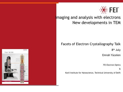
Imaging and analysis with electronsNew developments in TEMFacets of Electron <strong>Crystallography</strong> Talk8 th JulyEmrah Yücelen<strong>FEI</strong> Electron OpticsKavli Institute for Nanoscience, Technical University of Delft&
Titan Family in NanoresearchTitan ETEMTitan G2 60-300Titan 3 G2 60-3002STEM 10MxTEM 10 kx
Launch of the Titan G2 familyTechnical highlights• G2 family of Titan has been launched at M&M 2009• Redesign includes improvements <strong>FEI</strong> learned during the TEAM projectTechnical highlights• Voltage range extended to 60kV• Enhanced specifications in Cs-corrected STEM and TEMto 80pm level on Titan G2 60-300to 70pm level on Titan 3 G2 60-300(see specification table in new product data sheet)• X-FEG electron gun• New DCOR Probe Cs-corrector and electronics improvements• Cs-corrected field free imaging Lorentz microscopy3
20 nmFlexibility : Titan G2, not only a Corrector platformThe full functionality in S/TEM application is available…• 70pm in STEM and TEM at Titan 3 G2• SmartCam and enclosure to improve stability on Titan 3 G2• Full remote control operation with Collaboratory SW• X-FEG with highest analytical probe currents• Monochromator (100 Titans)with large reference user base
The optional X-FEG gun module on Titan G2• Product introduced since M&M 2008; >8 installed• Provides probe currents 250pA in a 0.2nm probe ona non Cs corrected Titans with a smaller probeconvergence angles to minimize the excitedvolume in the sample• 2000pA in a 0.2nm probe (Cs-corrected @ 300kV)• 1300pA in a 0.2nm probe (Cs-corrected @ 200kV)• Life time unchanged compared to S-FEG (
Performance with X-FEG/Probe Cs-corrector Titan at 300kVHAADF-STEM images on silicon with probe current/size measurement30mrad30mrad30mrad30mrad30mrad17mrad136pm 0.5nA6Measurement of the achievable currents in dependence of probe diameter of the X-FEGThe probe current varies from
New results on XFEG: outstanding holography performanceHR holography on gold grain boundaryHigh coherenceof the source20 nmImage of a parallel probe 2/409(5x better than Tecnai ICs)single hydrogen atomH 2/245M. Linck, B. Freitag, M. Lehmann submitted to Ultramicroscopy 20107Martin Linck, Michael Lehmann, Bert Freitag, Stephan Kujawa, Tore Niermann:Applied wave optics on the atomic scale: Electron holography materials characterization in a Titan TEM,Proc. MC2009, Vol. 1: Instrumentation and Methodology, Verlag der TU Graz 2009, 17-18.DOI 10.3217/978-3-85125-062-6-007.
Monochromator :Comparison Monochromator TEM with X-ray synchrotronon Ba 2 SiTi 2 O 8SynchrotronMonochromator TEMB.Freitag,<strong>FEI</strong>, Eindhoven, Dr Thomas Hoeche,Leibniz-Institute,Leipzig8• Energy resolution is as good as synchrotron• but with nanometer spatial resolution
Monochromator :EELS on polycarbonate at Helium temperatureO=CO-CC-HC-CC=CC=OProject with Hofer et al. Felmi, Graz, Austria9
SYNERGYX-FEGmono• X-FEG + Mono + C s -correction powerfulcombination• Ultimate…spatial resolutionenergy spreadhigh probe currentstability(NB: specs are for 300kV) TEM info limit < 70 pm STEM resolution < 70 pm 2 nA in 0.2 nm probe energy resolution 0.8eV 200pA in 0.2nm energy resolution < 0.2 eVcondensersystemprobecorrectorspecimen10
Mono/Image CsTEM information limit• X-FEG + Mono + C s -correctionpowerful combination• Ultimate…spatial resolutionenergy spreadhigh probe currentstability(NB: specs are for 300kV) TEM info limit < 70 pm STEM resolution < 70 pm 2 nA in 0.2 nm probe energy resolution < 0.2 eV1 2222Cc ΔV ΔE ΔII42 V V I 1 4Titan with image Cs-corrector and S-FEG (DE=0.7eV)Titan with image Cs-corrector and mono X-FEG (DE
Titan G2 performance exemplified in results:Best S/TEM resolution, analytics, and material scienceBest HR-S/TEM performance in the market (70pm)14Detailed description of the results in new applications brochure on Titan G2
Detect every signal at the same time :New <strong>FEI</strong> triple On-axis BF/DF detectorDeveloped by <strong>FEI</strong> and successfully introduced on Titane -One BF and two different DF detectors (DF2, DF4)• Can be used independently,i.e. BF and DF1/DF2 simultaneously• Optimized for combined use with EELS(signal is either collected by GIF/FS-1 or falls on DF detector)Accommodates higher currents (~3 nA) than Gatan 805/Fishioneplus simultaneous BF and DF imagingDF1DF2BFBFDF4HAADF15
Experimental ABF/HAADF STEM and HR-TEM imagesLaB 6 [100] specimenHR-TEMABFHAADFImages : S.Lazar,B.Freitag, <strong>FEI</strong>,J. Etheridge, Monash University, AustraliaLaBComparison between the different imaging techniques (HR-TEM/HR-STEM)on one material16
The new DCOR (dodecapole corrector)third generation probe Cs-correctorNew User interfaceelectronics cabinetBenefits :includes optical elements to correct higher order aberrations-> Allows for higher opening angles :Deep Sub-Ångström performance with wide pole piece gap (
„theoretical‟ comparisonthe impact of the higher order aberrations on probe shapeshexapole vs. DCORprobe C S correctorSimulations by Joerg Jinschekprogram: “Dr. Probe”by Juri Barthel (er-c, FZ Jülich)18
Ronchigram & probe shape simulations on DCOR and hexapole Cs-correctorwith guaranteed aberration numbers using new simulation SW Dr. ProbeHigher order aberration are higheron the hexapole than DCORand can be tuned by DCORtypical Hexapole100mrad30 mradDCOR Titan G2100mrad30 mradcalculated usingDr. Probeby Juri Barthel (FZ Jülich)sponsor: <strong>FEI</strong> CompanyDr. Probe SW available via <strong>FEI</strong> for owner platform H2 201019
hexapole probe corrector30 mrad probe200kVB2=0 nmA2=0 nmC3=±5 μmS3=±3 μmA3=±3 μmA4=30 μmB4=30 μmD4=30 μmC5=2000 μmA5=800 μm100mradTypical specifications for hexapole correctorsprogram: “Dr. Probe” by J. Barthel (er-c, FZ Jülich)20
DCOR probe corrector30 mrad probe200kVB2=0 nmA2=0 nmC3=±1 μmS3=±0.2 μmA3=±0.2 μmA4=5 μmB4=5 μmD4=5 μmC5=200 μmA5=200 μm21100mradconfidence level values for DCOR correctorsprogram: “Dr. Probe” by J. Barthel (er-c, FZ Jülich)
hexapole probe corrector30 mrad probe200kVB2=100 nmA2=0 nmC3=±5 μmS3=±3 μmA3=±3 μmA4=30 μmB4=30 μmD4=30 μmC5=2000 μmA5=800 μm100mradSpecification on B2 is 100nmYou cannot see it in the static Ronchigram!program: “Dr. Probe” by J. Barthel (er-c, FZ Jülich)22
DCOR probe corrector30 mrad probe200kVB2=30 nmA2=0 nmC3=±1 μmS3=±0.2 μmA3=±0.2 μmA4=5 μmB4=5 μmD4=5 μmC5=200 μmA5=200 μm23100mradDCOR level of confidence 30nmprogram: “Dr. Probe” by J. Barthel (er-c, FZ Jülich)
AGENDA• Flexibility24Confidential
FLEXIBILITY 3 condensers + minilens• 3-condenser zoom-systemcontrolled by Smart Optics TM• Beam parallelism andisoplanicity for a large rangeof TEM illuminationQuantitative 3 lens condenser system• Full control over probeconvergence in STEM,analysis, or CBEDExample :NBD,CBED, SAEDstrain analysis• NBD: parallel illuminationcan be restricted to 4nmdiameter at 300kV26
FLEXIBILITYDe-scan on every Titan standard• De-scan; Why is it important?• EELS: no ZL-peak energy shift duringSI acquisition• New imaging techniquesgoing public at M&M/IMC2010• SCEM , confocal micorscopy(atomic 3D)De-scan activeNo de-scan27
FLEXIBILITYHT range from 60 to 300kV• Can balance effects of• Knock-on damage vs. radiolysis• Contrast vs. penetration• Cross-section vs. brightness• Energy spread vs. brightness& resolutionSWCNTbeam-sensitive materialsTEM imaging, tomographyEDS & EELSEELSGe2 n mAu nanoparticlesYoung fringesAmorphous C-filmMulti wall CNTSingle wall CNTCNT type 1CNT type 2Amorphous C-filmBonding state analysis at 80kV0 . 5 n mAtomic resolution at 60kV100 pm28
Inelastic MFP [nm]Theoretical Consideration: Sample Penetration/interactioninelastic and inelastic scattering dependence on atomic number and high tensionInelastic MFP dependence on HTinelastic MFP dependence on z200300kV200kV1501005003 23 43 63 83Atomic Number [Z}Mean-free-path dependence on high-tension foraluminum and carbon. The MFP increases by 20-30%from 200kV to 300kV.Inelastic mean-free path calculated for amorphousmaterials with different average atomic number Zat 200 kV and 300kV.The MFP increases by 20-30% from 200kV to 300kV.29
HR-TEM on gold nanoparticles on carbon filmTITAN image corrected with 80,200,300kV80kV200kV300kV2 n m• Cs-corrected images on one instrument at the same area with different acceleration voltages• At heavy elements 300kV shows the clearest image of the surface• At 80kV the carbon contrast is maximized and a step in thickness in the center of theparticle becomes visibleE Yücelen Ph.D. Thesis (<strong>FEI</strong>)30
Practical benefit of 300kV on carbon support film samples :Pt clusters and single atoms on thin carbon support filmTitan 80-300 with image Cs-corrector at 300kVSingle atoms and Sub NanometerPt-clusters can be image artifactfree due to the high penetrationpower of the electrons at 300kVacceleration voltage.The carbon support film is almostas invisible and as transparent asthe hole in the film (upper rightcorner)Only possible with 300kVImages : Dr. R. Schneider, Laboratory for Electron Microscopy Universität Karlsruhe (TH)Sample : Dr. A. Byier, Universität Bielefeld, Holger Blank (LEM, Universität Karlsruhe)31 31
The Need for High Tension FlexibilityFresh areasame area after 1min in e-beamDamaged tubes5 n mImages : B.Freitag, sample : Prof Kiselev, Moscow, Russia5 n m32Atomic resolution images of C-single wall nano-tubes with CuI filling @ 300kV shows beam damageafter ~1-2min in the e-beam
Seeing Linked Structures: Titan at 80kV2 n m2 n mAtomic resolution at 80kV with ultra stable conditions and high contrast for SWCNTThe delicate relationship between the tubes and the surface carbon can be studied withatomic resolution.33
Atomic 3D on graphen double and single layersusing new Trueimage Atlas SW atExperimentatomic modelFocus series at 80kVCarbon dumbbell can be resolved at 80kV• Atomic positions of 2 carbon atomsand single carbon atom can bedistinguishedsimulation• Atomic 3D information can be obtained• Different heights of single atoms can bemeasured (3A)34Joerg R. Jinschek, Emrah Yucelen, Hector A. Calderon, Bert Freitag, Quantitative atomic 3-D imaging of single/double sheet graphenestructure, Carbon, Volume 49, Issue 2, February 2011, Pages 556-562, ISSN 0008-6223, DOI: 10.1016/j.carbon.2010.09.058.
Beam damage : not everything is knock-on damageImage : B. Freitag , <strong>FEI</strong>; R.Erni, NCEM, Berkeley• Grain boundary flip in gold 110 in HR-STEM imaging.• Surface migration of gold atoms; melting of CuI crystal in SWCNT• Mechanisms unclear…• Knock- on damage energy is different in bulk than on grain boundary or surface35
AGENDAEELSChemical information on the atomic level36Confidential
Atomic HR-STEM/EELS on BaTiO 3 /SrTiO 3 interfaceADFEELS map 80kV,46x46pix, 30ms/pixBaTiBaSrAtomically sharp interfaceshows minimumdelocalization by atomicresolved EELSSr37Gianluigi A. Botton, Sorin Lazar, Christian Dwyer, Elemental mapping at the atomic scale using low accelerating voltages,Ultramicroscopy, Volume 110, Issue 8, PROCEEDINGS OF THE INTERNATIONAL WORKSHOP ON ENHANCED DATA GENERATEDBY ELECTRONS, July 2010, Pages 926-934, ISSN 0304-3991,
e-Where does the delocalization come from?<strong>Open</strong>ing angle &sample thickness, 3D probe geometry2D Probe shape in Vacuum3D volume in sample with thickness t excited by probe24022020018016014010 mrad30 mrad120100806040b = t 2 tan 2000 . 2 n m0.20 0.25 0.30 0.35 0.40 0.45 0.50 0.55 0.60 0.65nmAverage FWHM of 77pm ( in vacuum)Filtered STEM , energy resolution of 0.15eVtbExample b = 30nmx 2x 0.03 = 1.8nm= 5nmx 2x 0.03 = 0.3nmttbThe higher the opening angle, the bigger the current (signal) ,but on real sample (t/l~ 0.3 ~ 30-50nm) the bigger the excited volume38Direct measurement of the smallest probe diameter in 2D shows Sub Ångström size,but the electron probe has limited focal depth due to the opening angle,which leads to cross talk in atomic spectroscopyTherefore the excited volume increases with opening angle and sample thickness
Where does the cross talk come from?Bloch wave delocalization (Channeling/de-channeling) in SrTiO 3HAADF STEM imageSearch HAADFLine-scan of the image the probeacross SrTiO 3Search CCD300kV = 10mradImage Cs-correctedThickness ~0.38MFP2 nm1nm500 nmB.Freitag,C.Mitterbauer, <strong>FEI</strong>39Imaging the electron probe on the specimen with an image Cs-correctorshows wide distribution of electrons in the real space.The next neighboring atoms are illuminated by the electrons (channeling/de-channeling)
Where does the cross talk come from and how can we influence it?Spectroscopy performance : EELS map on SrTiO3 at 80kVSTEM/EELS mapsRatio between elastic to inelastic scattering factors in /s elSrTi31.20.75ORGBGianluigi A. Botton, Sorin Lazar, Christian Dwyer, Elemental mapping atthe atomic scale using low accelerating voltages, Ultramicroscopy,Volume 110, Issue 8, PROCEEDINGS OF THE INTERNATIONALWORKSHOP ON ENHANCED DATA GENERATED BY ELECTRONS,July 2010, Pages 926-934, ISSN 0304-3991,40Atomic STEM/EELS map at 80kV is possible (resolution ~0.4nm)Lower voltage improves sensitively (cross sections), higher voltage minimizes excited volume (convergence angle)But the ratio between elastic and inelastic scattering factor is varying greatly with atomic numberWhich signal is chemical, which is elasic? Simulations& more experiments…required
Tecnai Osiris TM : Super-X• Silicon Drift Detectors (SDD) replace thelithium drifted silicon (Si(Li)) detectors<strong>FEI</strong> designed a new detector within a new pole piecefor ultimate performance in EDS analysis in a S/TEM(patent pending).Benefits of new <strong>FEI</strong> design:- Collection angle: 0.9 srad 3-7 times more than existing- Throughput rate >240 kcps ~5 times more- Pixel dwell time for mapping down to 10 μs/pixel >1000x faster- Windowless design (with shutters) Higher sensitivity forlight elements (N,O,B, etc.)- Energy resolution
Output Count Rate [kcps]Super-X Detector: SDD BasicsDetector designSDD max. output count rate is muchhigher than for standard Si(Li)OutputCountRate[kcps]250200Measured Count/s versus Input Count/sXFlash Detector 3001SDDQUANTAX , high speed150concept patented by Kemmer & Lutz in 198910050Si(Li)Competitor A, high speed,00 100 200 300 400 500 600 700 800 900 1000Input Count Rate [kcps]Input Count Rate [kcps]SDD advantage :low capacitance = high throughput= low dead time at high count rates42An integrated multiple silicon drift detector system for transmission electron microscopesH S von Harrach et al 2010 J. Phys.: Conf. Ser. 241 012015
normalised count rateSuper-X Detector on OsirisTEM PCBruker signalprocessorRelative count rate at 200kV, NiOx film,constant probe currentPNSensor SDD(4x)Vacuum feed through1.210.80.60.40.20Shutter-30 -20 -10 Lower pole0 10 20 30Cold trapalpha tilt angleSuperXSi(Li) 0.3 srLiquid N 2dewar• 4 Silicon Drift Detectors (SDD) symmetrically around sample :120 mm 2 detector area• 0.9 srad collection angle with symmetric design allowing for tilt flexibility in EDS• Enhanced sensitivity for light elements• 200,000 cps (output) were measured• Dwell times per pixel down to 10 µs, i.e. 100,000 spectra/sec43Microscopy Today (2010), 18:14-20 Cambridge University Press
kcpskcpsSuper-X Performance on Tecnai OsirisThe benefit of collection angle improvementand higher throughput of SSD technology700506004030Measured input counts50020100.3 sr Si(Li) plus Schottky FEG40030020000 0.2 0.4 0.6 0.8 1Beam current [nA]Super-X plus X-FEGIn both experimentsthe same FIB-cut InP samplewas usedwith a thickness of about 200 nm.100Calculated output counts00 2 4 6 8 10 12 14Beam current [nA]Higher sensitivity of the design allow for more X-ray counts per electron (nA)than any other EDS detector on a S/TEM44Microscopy Today (2010), 18:14-20 Cambridge University Press
Super-X: SDD Technology and Fast Mapping• Enhanced sensitivity for light elements• 300,000 cps (output) were measured• Dwell times per pixel down to 10 µs, i.e. 100,000 spectra/sec• Mapping time reduced from 2 hr to 2 minutes• Speed can also be traded in for larger maps (more pixels):larger field-of-view45
Super-X Detector: Light Element Detection40000350003000025000O-K Ni-Lwindowless SDDSi(Li)Ni-K20000150001000050000C-K0 1 2 3 4 5 6 7 8NiO x film on carbon, 200 kVkeVWindowless detector has more transmissivity for low-energy X-rays,e.g. ~3x more signal for O-K than with Moxtek window46Microscopy Today (2010), 18:14-20 Cambridge University Press
Fast Mapping with Super-X: FinFETComparison of Tecnai Osiris with TF20 XTHAADF STEMSi K Hf L Ti KTecnai TF20XTNi K O K N K100 x 100 pixel500 msec dwell time~0.7 nm spot, 0.4 nA1 h 54 min total time ~ 2 hrsFull quantificationImages and maps by A. Carlsson, <strong>FEI</strong>HAADF STEMSi K Hf L Ti KTecnai Osiris (X-FEG, Super-X)Ni K O K N K100 x 100 pixel5 msec dwell time~0.3 nm spot, 1 nA115 sec total time ~ 2 minFully quantified (binning 2)Sample courtesy of NXP ResearchImages and maps by D. Klenov, <strong>FEI</strong>47http://www.fei.com/products/transmission-electron-microscopes/tecnai/osiris.aspx
Super_X : Minimum mass fraction (MMF) limitsNew record on certified NIST steel No 46149Beat the best AEM results of Watanabe&Williams UM 78 (1999) in MMF on Cu 0.12wt%Mn
MMF performance versus spatial resolutionExample chemical detection of As dopant profile in siliconSemi conducting deviceOsirisWatanabe et al. Micro.&Microanal.12 2006As dopant ~ 10 -19 ~0.03wt%Lateral resolution ~ 5nmEstimate :1 atom in a volume exitedWith a 1nm probe sizeof a 100nm thick samplewill become detectable!!!600x600 pix, 50 sec dwell time, multiple frames,78 min total time, 2.2 nA, drift corr50
51Atomic EDS: How does it compare to EELS?SiLi conventional detector results
Super-X on Titan G2 60-300• 4 Silicon Drift Detectors (SDD) symmetrically around sample :120 mm 2 detector area• 0.7 srad collection angle with symmetric design allowing for tilt flexibility in EDS• Enhanced sensitivity for light elements• 200,000 cps (output) were measured• Dwell times per pixel down to 10 µs, i.e. 100,000 spectra/sec• Patent pending• Super-X on Titan has high sensitivity like Osiris, but additionally• high spatial resolution for atomic EDS (due to Cs-correction)• atomic resolution at low voltage (less knock-on damage)• Tecnai speed-> Osiris from hours to minutesTitanspeed->Probe Cs-corrected/XFEG from minutes to seconds52
Electron Diffraction on TITANTITAN 3-condenser lens system provides wide range of possibilities fordiffraction experiments:•Nano size paralell beam.•Variable beam convergence for fixed aperture sizeNano size coherent parallel electronbeam formation:•Nanoprobe mode or MicroprobeMode•Choice of small C2 apertures 20umto 5um.•High Spot numbers and Strong Gunlens settings53
what is new: Precession Electron DiffractionAvailable with TITAN SW 1.2 (release mid 2011)Controlled from TITAN user interface54
BeamDeflectionCoilsIn TITAN SWDynamical Conical DarkField Alignments:Adjust Pivot Pointsandcorrects distortions inDiffraction modeImageDeflectionCoilsBack Focal PlaneTITAN SW 1.2 (will berelaesed end of 2010)Activation of De-scan:Beam movement ismade stationaryDiffraction ModeE Yücelen Ph.D. Thesis (<strong>FEI</strong>)55
(Ba , Na) 3 Nb 5 O 15 Crystal seen along c directiona=1.759nmb=1.762nmc=0.3995nmSpace group Cmm2Experimentalmethods to acquiredata for electroncrystallographyE Yücelen Ph.D. Thesis (<strong>FEI</strong>)56
(Ba , Na) 3 Nb 5 O 15 Kinematical Diffraction pattern seen along [001] directionE Yücelen Ph.D. Thesis (<strong>FEI</strong>)57Simulations using JEMS by Prof. Stadelmann
Recording Images on FLUCAM20 nm 20 nmE Yücelen Ph.D. Thesis (<strong>FEI</strong>)58
Beam Profile2 0 n mMicroprobe modeBeam size at FWHM is 4.5nmE Yücelen Ph.D. Thesis (<strong>FEI</strong>)59
Nano Beam Diffractionwith4.5nm focused electron beamNano Beam Diffractionwith35nm parallel electron beamE Yücelen Ph.D. Thesis (<strong>FEI</strong>)60
Nano Beam Diffraction with 4.5nm focused electron beamHelp by activatingDark Field Modeandaccessing beam tiltto achieve nearZone axisConvergence semi angle lower than 1mradE Yücelen Ph.D. Thesis (<strong>FEI</strong>)61
Nano Beam Diffraction PatternPrecession Diffraction PatternPrecession Angle is 50 mradE Yücelen Ph.D. Thesis (<strong>FEI</strong>)62
EFTEM Thickness Maps1 23 4E YücelenPh.D. Thesis(<strong>FEI</strong>)63
Thickness Maps: Profiles1 23 464Thickness change drastically within 20 nm!E Yücelen Ph.D. Thesis (<strong>FEI</strong>)
Structure ImagingUsing HRTEMWhere are atoms?65E Yücelen Ph.D. Thesis (<strong>FEI</strong>)
Phase of theexit waveExit waveReconstructionAfter processing20 HRTEM2k x 2k imagesNb, O, Ba columnsandNa/Ba columnscan be identifiedInPhase image ofElectron Exit waveE Yücelen Ph.D. Thesis (<strong>FEI</strong>)66
Amplitude of theexit waveE Yücelen Ph.D. Thesis (<strong>FEI</strong>)67
HAADF STEMNon Probe Corrected TITANE Yücelen Ph.D. Thesis (<strong>FEI</strong>)68
Acknowledgements• Dr. Bert Freitag• Dr. Stephan Kujuwa• Dr. Joerg Jinschek• Dr. Jouk Janssen (TU Delft)• Prof. Henny Zandbergen (TU Delft)69