AM/FM tuner for car radio hifi applications - STMicroelectronics
AM/FM tuner for car radio hifi applications - STMicroelectronics
AM/FM tuner for car radio hifi applications - STMicroelectronics

Create successful ePaper yourself
Turn your PDF publications into a flip-book with our unique Google optimized e-Paper software.
<strong>FM</strong>-PART<br />
■ RF AGC GENERATION BY RF AND IF<br />
DETECTION FOR PIN DIODES AND MOSFET<br />
(PRESTAGE)<br />
■ 1 ST MIXER FOR 1ST <strong>FM</strong> IF 10.7MHz WITH<br />
PROGR<strong>AM</strong>MABLE IF TANK ADJUST FOR <strong>FM</strong><br />
AND <strong>AM</strong> UPCONVERSION<br />
■ 2 PROGR<strong>AM</strong>MABLE IF-GAIN STAGES<br />
■ 2 ND MIXER FOR 2ND IF 450KHz<br />
■ INTERNAL IF BANDPASS FILTER WITH<br />
THREE BANDWIDTHS CONTROLLED BY ISS<br />
(INCLUDING WEATHER BAND)<br />
■ FULLY INTEGRATED <strong>FM</strong>-DEMODULATOR<br />
<strong>AM</strong>-PART<br />
■ WIDE AND NARROW AGC GENERATION<br />
■ PRE<strong>AM</strong>PLIFIER AND MIXER FOR 1ST IF<br />
10.7MHZ,<br />
<strong>AM</strong> UPCONVERSION<br />
■ 2 ND MIXER FOR 2ND IF 450KHZ<br />
■ INTEGRATED <strong>AM</strong>-DEMODULATOR<br />
■ OUTPUT FOR <strong>AM</strong>-STEREO-DECODER<br />
ADDITIONAL FEATURES<br />
■ HIGH PERFORMANCE FAST PLL FOR RDS-<br />
SYSTEM<br />
■ IF COUNTER FOR <strong>FM</strong> AND <strong>AM</strong><br />
UPCONVERSION WITH SEARCH STOP<br />
SIGNAL<br />
■ QUALITY DETECTOR FOR LEVEL,<br />
DEVIATION, ADJACENT CHANNEL AND<br />
November 2001<br />
MULTIPATH<br />
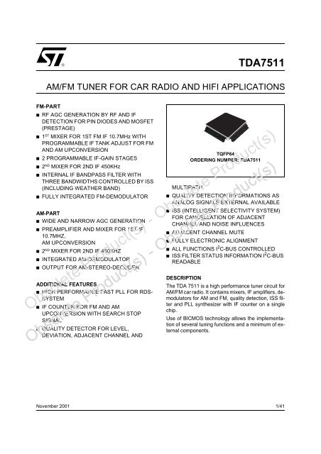
TDA7511<br />
<strong>AM</strong>/<strong>FM</strong> TUNER FOR CAR RADIO AND HIFI APPLICATIONS<br />
TQFP64<br />
ORDERING NUMBER: TDA7511<br />
■ QUALITY DETECTION INFORMATIONS AS<br />
ANALOG SIGNALS EXTERNAL AVAILABLE<br />
■ ISS (INTELLIGENT SELECTIVITY SYSTEM)<br />
FOR CANCELLATION OF ADJACENT<br />
CHANNEL AND NOISE INFLUENCES<br />
■ ADJACENT CHANNEL MUTE<br />
■ FULLY ELECTRONIC ALIGNMENT<br />
■ ALL FUNCTIONS I 2 C-BUS CONTROLLED<br />
■ ISS FILTER STATUS INFORMATION I 2 C-BUS<br />
READABLE<br />
DESCRIPTION<br />
The TDA 7511 is a high per<strong>for</strong>mance <strong>tuner</strong> circuit <strong>for</strong><br />
<strong>AM</strong>/<strong>FM</strong> <strong>car</strong> <strong>radio</strong>. It contains mixers, IF amplifiers, demodulators<br />
<strong>for</strong> <strong>AM</strong> and <strong>FM</strong>, quality detection, ISS filter<br />
and PLL synthesizer with IF counter on a single<br />
chip.<br />
Use of BICMOS technology allows the implementation<br />
of several tuning functions and a minimum of external<br />
components.<br />
Obsolete Product(s) - Obsolete Product(s)<br />
Obsolete Obsolete Product(s) Product(s) - - Obsolete Obsolete Product(s) Product(s)<br />
1/41
TDA7511<br />
BLOCK DIAGR<strong>AM</strong><br />
Obsolete Obsolete Product(s) Product(s) - - Obsolete Obsolete Product(s) Product(s)<br />
2/41<br />
<strong>AM</strong>IFin<br />
25 26 33 36 51 49<br />
57 59 54 52 50 46 45<br />
53<br />
61 62 60<br />
5<br />
6<br />
48<br />
V V CC1 CC2<br />
Supply<br />
I 2 C Bus<br />
11<br />
AGC<br />
REF<br />
Dem<br />
S-Meter 10.7MHz<br />
Divider<br />
MPX<br />
Dem<br />
450KHz<br />
Adjacent Channel<br />
Detection<br />
Multipath<br />
Detection<br />
Deviation<br />
Detection<br />
IFC<br />
PLL<br />
PD<br />
+<br />
VCO<br />
Soft/AC<br />
Mute<br />
CP<br />
AF<br />
ISS<br />
Xtal<br />
7<br />
9<br />
8<br />
16<br />
18<br />
19<br />
17<br />
30<br />
31<br />
32<br />
28<br />
10<br />
12<br />
<strong>FM</strong><br />
35<br />
44<br />
47<br />
PIN<br />
Logic<br />
42<br />
37<br />
+<br />
DAGC<br />
Divider<br />
PIN<br />
Dem<br />
1<br />
<strong>AM</strong><br />
S-Meter<br />
2<br />
Stopstation<br />
34<br />
MUX<br />
WAGC<br />
3<br />
4<br />
64<br />
15 43 38 39 41 40<br />
27 23 20 21 22 24 58 14 55 56 20 13<br />
63<br />
<strong>AM</strong>IF1in<br />
Obsolete Product(s) - Obsolete Product(s)<br />
V CC3<br />
99AT0052
PIN CONNECTION (Top view)<br />
99AT0053<br />
PIN DESCRIPTION (continued)<br />
<strong>AM</strong>PINDR<br />
GNDVCO<br />
<strong>AM</strong>RFAGCTC<br />
VCOB<br />
MIX1OUT1<br />
VCOE<br />
N° Pin Function<br />
1 <strong>AM</strong>MIX1IN2 <strong>AM</strong> Input2 Mixer1<br />
2 <strong>AM</strong>MIX1IN1 <strong>AM</strong> Input1 Mixer1 Reference<br />
3 <strong>AM</strong>RFAGCIN Input <strong>AM</strong> RF AGC<br />
4 <strong>AM</strong>RFAGCOUT Output <strong>AM</strong> RF AGC<br />
5 <strong>FM</strong>PINDR <strong>FM</strong> PIN Diode Driver Output<br />
6 <strong>FM</strong>MOSDR <strong>FM</strong> MOS Driver Output<br />
7 <strong>FM</strong>MIX1IN1 <strong>FM</strong> Input1 Mixer1<br />
8 GNDRF RF Ground<br />
9 <strong>FM</strong>MIX1IN2 <strong>FM</strong> Input2 Mixer1<br />
10 TV1 Tuning Voltage 1<br />
11 <strong>FM</strong>RFAGCIN <strong>FM</strong> RF AGC Input<br />
12 TV2 Tuning Voltage 2<br />
13 ADJCH Ident. Adjacent Channel Output<br />
14 FSU Unweighted Fieldstrength Output<br />
MIX1OUT2<br />
DEVTC<br />
<strong>FM</strong>IFAGCIN<br />
XTALD<br />
GNDIF<strong>AM</strong>P<br />
XTALG<br />
<strong>AM</strong>IF1IN<br />
TDA7511<br />
Obsolete Obsolete Product(s) Product(s) - - Obsolete Obsolete Product(s) Product(s)<br />
<strong>FM</strong><strong>AM</strong>P1IN<br />
64 63 62 61 60 59 58 57 56 55 54 53 52 51 50 49<br />
<strong>AM</strong>MIX1IN2 1<br />
48 VREF1<br />
<strong>AM</strong>MIX1IN1 2<br />
47 GNDDEM<br />
<strong>AM</strong>RFAGCIN 3<br />
46 <strong>FM</strong>MIX2IN1<br />
<strong>AM</strong>RFAGCOUT 4<br />
45 <strong>FM</strong>MIX2IN2<br />
<strong>FM</strong>PINDR 5<br />
44 <strong>FM</strong>DEMC<br />
<strong>FM</strong>MOSDR 6<br />
43 <strong>AM</strong>IF2IN<br />
<strong>FM</strong>MIX1IN1 7<br />
42 MUTETC<br />
GNDRF 8<br />
41 <strong>AM</strong>DETC<br />
<strong>FM</strong>MIX1IN2 9<br />
40 <strong>AM</strong>AGC2TC<br />
TV1 10<br />
39 <strong>AM</strong>IFBPF<br />
<strong>FM</strong>RFAGCIN 11<br />
38 <strong>AM</strong>IFREF<br />
TV2 12<br />
37 MPX/AF<strong>AM</strong><br />
ADJCH 13<br />
36 VCC1<br />
FSU 14<br />
35 FSW<br />
ISSTC 15<br />
34 <strong>AM</strong>ST/MP<br />
VCCVCO 16<br />
33 GNDVCC1<br />
17 18 19 20 21 22 23 24 25 26 27 28 29 30 31 32<br />
<strong>AM</strong>MIX2OUT1<br />
<strong>AM</strong>MIX2OUT2<br />
<strong>FM</strong><strong>AM</strong>P1OUT<br />
<strong>FM</strong>IF1REF<br />
<strong>FM</strong><strong>AM</strong>P2IN<br />
VCC2<br />
<strong>FM</strong><strong>AM</strong>P2OUT<br />
GNDVCC2<br />
GNDVCC3<br />
SSTOP<br />
SDA<br />
SCL<br />
VCC3<br />
LPOUT<br />
VREF2<br />
LP<strong>AM</strong><br />
LP<strong>FM</strong><br />
LPHC<br />
Obsolete Product(s) - Obsolete Product(s)<br />
3/41
TDA7511<br />
PIN DESCRIPTION (continued)<br />
N° Pin Function<br />
Obsolete Obsolete Product(s) Product(s) - - Obsolete Obsolete Product(s) Product(s)<br />
4/41<br />
15 ISSTC Time Constant <strong>for</strong> ISS Filter Switch<br />
16 VCCVCO VCO Supply<br />
17 GNDVCO VCO Ground<br />
18 VCOB VCO Input Base<br />
19 VCOE VCO Output Emitter<br />
20 DEVTC Deviation Detector Time Constant<br />
21 XTALD Xtal Oscillator to MOS Drain<br />
22 XTALG Xtal Oscillator to MOS Gate<br />
23 GNDVCC3 VCC3 Ground<br />
24 SSTOP Search Stop Output<br />
25 SDA I 2 C-Bus Data<br />
26 SCL I2C-Bus Clock<br />
27 VCC3 Supply Tuning Voltage<br />
28 LPOUT Op Amp Output to PLL Loop Filters<br />
29 VREF2 Voltage Reference <strong>for</strong> PLL Op Amp<br />
30 LP<strong>AM</strong> Op Amp Input to PLL Loop Filters <strong>AM</strong><br />
31 LP<strong>FM</strong> Op Amp Input to PLL Loop Filters <strong>FM</strong><br />
32 LPHC High Current PLL Loop Filter Input<br />
33 GNDVCC1 Digital Ground<br />
34 <strong>AM</strong>ST/MP <strong>AM</strong> Stereo Out / Ident. Multipath Output<br />
35 FSW Weighted Fieldstrength Output<br />
36 VCC1 Digital Supply<br />
37 MPX/AF<strong>AM</strong> MPX Output / <strong>AM</strong> AF Output<br />
38 <strong>AM</strong>IFREF Reference Voltage <strong>AM</strong> IF Amp<br />
39 <strong>AM</strong>IFBPF <strong>AM</strong> IF Filter<br />
40 <strong>AM</strong>AGC2TC <strong>AM</strong> AGC2 Time Constant<br />
41 <strong>AM</strong>DETC <strong>AM</strong> Detector Capacitor<br />
42 MUTETC Softmute Time Constant<br />
43 <strong>AM</strong>IF2IN Input <strong>AM</strong> IF2<br />
44 <strong>FM</strong>DEMC <strong>FM</strong> Demodulator Reference<br />
45 <strong>FM</strong>MIX2IN2 <strong>FM</strong> IF1 MIX2 Input1<br />
46 <strong>FM</strong>MIX2IN1 <strong>FM</strong> IF1 MIX2 Input2<br />
47 GNDDEM Ground <strong>FM</strong> Demodulator<br />
48 VREF1 Reference 5V<br />
49 GNDVCC2 Analog Ground<br />
50 <strong>FM</strong><strong>AM</strong>P2OUT <strong>FM</strong> IF1 Amplifier2 Output<br />
Obsolete Product(s) - Obsolete Product(s)
PIN DESCRIPTION (continued)<br />
N° Pin Function<br />
51 VCC2 Analog Supply<br />
52 <strong>FM</strong><strong>AM</strong>P2IN <strong>FM</strong> IF1 Amplifier2 Input<br />
53 <strong>FM</strong>IF1REF <strong>FM</strong> IF1 Amplifier Reference<br />
54 <strong>FM</strong><strong>AM</strong>P1OUT <strong>FM</strong> IF1 Amplifier1 Output<br />
55 <strong>AM</strong>MIX2OUT2 <strong>AM</strong> Tank 450kHz<br />
56 <strong>AM</strong>MIX2OUT1 <strong>AM</strong> Tank 450kHz<br />
57 <strong>FM</strong><strong>AM</strong>P1IN <strong>FM</strong> IF1 Amplifier1 Input<br />
58 <strong>AM</strong>IF1IN <strong>AM</strong> IF1 Input<br />
59 GNDIF1<strong>AM</strong>P <strong>FM</strong> IF1 Amplifier Ground<br />
60 <strong>FM</strong>IF1AGCIN <strong>FM</strong> IF1 AGC Input<br />
61 MIX1OUT2 MIX Tank 10.7MHz<br />
62 MIX1OUT1 MIX Tank 10.7MHz<br />
63 <strong>AM</strong>RFAGCTC <strong>AM</strong> RF AGC Time Constant<br />
64 <strong>AM</strong>PINDR <strong>AM</strong> PIN Diode Driver Output<br />
ABSOLUTE MAXIMUM RATINGS<br />
THERMAL DATA<br />
TDA7511<br />
Symbol Parameter Value Unit<br />
VS Supply Voltage 10.5 V<br />
Tamb Ambient Temperature -40 to 85 °C<br />
Tstg Storage Temperature -55 to +150 °C<br />
Symbol Parameter Value Unit<br />
RTh(j-amb) Thermal resistance 68 °C/W<br />
Obsolete Product(s) - Obsolete Product(s)<br />
ELECTRICAL CHARACTERISTCS<br />
Tamb = +25°C, VCC1 = VCC2 = VCC3 = VCCVCO = VCCMIX1 = 8.5V, fRF = 98MHz, dev. = 40kHz,<br />
fMOD =1kHz, fIF1 = 10.7MHz, fIF2 = 450KHz, fXtal = 10.25MHz, in test or application circuit, unless otherwise<br />
specified.<br />
Obsolete Obsolete Product(s) Product(s) - - Obsolete Obsolete Product(s) Product(s)<br />
Symbol<br />
Supply<br />
Parameter Test Condition Min. Typ. Max. Unit<br />
VCC1 Digital supply voltage 7.5 8.5 10 V<br />
VCC2 Analog supply voltage 7.5 8.5 10 V<br />
VCC3 Analog tuning voltage 7.5 8.5 10 V<br />
VCCVCO VCO supply voltage 7.5 8.5 10 V<br />
5/41
TDA7511<br />
ELECTRICAL CHARACTERISTCS (continued)<br />
Tamb = +25°C, VCC1 = VCC2 = VCC3 = VCCVCO = VCCMIX1 = 8.5V, fRF = 98MHz, dev. = 40kHz,<br />
fMOD =1kHz, fIF1 = 10.7MHz, fIF2 = 450KHz, fXtal = 10.25MHz, in test or application circuit, unless otherwise<br />
specified.<br />
Symbol Parameter Test Condition Min. Typ. Max. Unit<br />
VCCMIX1 MIX1 supply voltage 7.5 8.5 10 V<br />
VCCMIX2 MIX2 supply voltage 7.5 8.5 10 V<br />
Obsolete Obsolete Product(s) Product(s) - - Obsolete Obsolete Product(s) Product(s)<br />
6/41<br />
ICC1 Supply current <strong>FM</strong> ON 7.5 mA<br />
ICC1 Supply current <strong>AM</strong> ON 10 mA<br />
ICC2 Supply current <strong>FM</strong> ON 50 mA<br />
ICC2 Supply current <strong>AM</strong> ON 60 mA<br />
ICC3 Supply current 2 mA<br />
ICCVCO Supply current 2.5 mA<br />
ICCMIX1 Supply current <strong>FM</strong> ON 6 mA<br />
ICCMIX1 Supply current <strong>AM</strong> ON 5 mA<br />
ICCMIX2 Supply current <strong>AM</strong> ON 5 mA<br />
Reference Voltages<br />
VREF1 Internal reference voltage IREF1 = 0mA 5 V<br />
VREF2 Internal reference voltage IREF2 = 0mA 2.5 V<br />
Wide Band RF AGC<br />
V11 Threshold AGC start V6 = VCC2/2 80 dBμV<br />
RIN Input resistance 500 Ω<br />
CIN Input capacitance 2.5 pF<br />
Narrow Band RF & Keying AGC<br />
V60 Lower threshold <strong>FM</strong>AGC, V11 = 0mVRMS 82 dBμV<br />
V60 Upper threshold <strong>FM</strong>AGC, V11 = 0mVRMS 92 dBμV<br />
RIN Input resistance 10 kΩ<br />
CIN Input capacitance 2.5 pF<br />
Obsolete Product(s) - Obsolete Product(s)<br />
AGC MOSFET Driver Output<br />
V6 Max. AGC output voltage V11 = 0mVRMS VCC2<br />
-0.5V<br />
V6 Min. AGC output voltage V11 = 50mVRMS 0.5 V<br />
I6 Min. AGC charge current V11 = 0mVRMS,V6 = VCC2/2 -12.5 μA<br />
I6 Max. AGC discharge current V11 = 50mVRMS,V6 = VCC2/2 1.25 mA<br />
AGC PIN Diode Driver Output<br />
I5 AGC OUT, current min. V11 = 0mVRMS, V5 = 2V 50 μA<br />
I5 AGC OUT, current max. V11 = 50 mVRMS, V5 = 2V -6 mA<br />
Mixer1 (10.7MHz)<br />
RIN Input impedance Balanced, f = 98MHz 9 Ω<br />
V
TDA7511<br />
ELECTRICAL CHARACTERISTCS (continued)<br />
Tamb = +25°C, VCC1 = VCC2 = VCC3 = VCCVCO = VCCMIX1 = 8.5V, fRF = 98MHz, dev. = 40kHz,<br />
fMOD =1kHz, fIF1 = 10.7MHz, fIF2 = 450KHz, fXtal = 10.25MHz, in test or application circuit, unless otherwise<br />
specified.<br />
Symbol Parameter Test Condition Min. Typ. Max. Unit<br />
IP3 3rd order intercept point 122 dBμV<br />
F Noise figure 6 dB<br />
AC Conversion gain 120 mS<br />
IF1 Amplifier1 & 2 (10.7MHz)<br />
Amin Min. gain IFG 9 dB<br />
Amax Max. gain IFG 15 dB<br />
RIN Input resistance 330 Ω<br />
ROUT Output resistance 330 Ω<br />
P1dB 1dB compression point Output referred 120 dBμV<br />
IP3 3rd order Intercept Point Output referred 132 dBμV<br />
Mixer2 (450kHz)<br />
RIN Input impedance 330 Ω<br />
V46 Max. input voltage 900 mVRM<br />
S<br />
V48 Limiting sensitivity S/N = 20dB 25 μV<br />
A Mixer gain 18 dB<br />
Limiter 1 (450kHz)<br />
GLimiter Gain 80 dB<br />
Demodulator, Audio Output<br />
THD Dev.= 75kHz, V46 = 10mVRMS 0.1 %<br />
VMPX MPX output signal Dev.= 75kHz 500 mVRM<br />
S<br />
ROUT Output resistance 350 Ω<br />
|ΔV|min DC offset fine adjust DEM, MENA=1 6 mV<br />
Obsolete Product(s) - Obsolete Product(s)<br />
|ΔV|max DC offset fine adjust DEM, MENA=1 186 mV<br />
S/N Dev.= 40kHz,V46 = 10mVRMS 75 dB<br />
Quality Detection<br />
S-meter, Unweighted Fieldstrength<br />
Obsolete Obsolete Product(s) Product(s) - - Obsolete Obsolete Product(s) Product(s)<br />
V46 Min. input voltage MIX2 10 μV<br />
ΔV Per decade SMSL = 0 1 V<br />
ΔV Per decade SMSL = 1 1.5 V<br />
V14 Fieldstrength output V46 = 0VRMS 0.1 V<br />
V14 Fieldstrength output V46 = 1VRMS 4.9 V<br />
ROUT Output resistance 4 kΩ<br />
7/41
TDA7511<br />
ELECTRICAL CHARACTERISTCS (continued)<br />
Tamb = +25°C, VCC1 = VCC2 = VCC3 = VCCVCO = VCCMIX1 = 8.5V, fRF = 98MHz, dev. = 40kHz,<br />
fMOD =1kHz, fIF1 = 10.7MHz, fIF2 = 450KHz, fXtal = 10.25MHz, in test or application circuit, unless otherwise<br />
specified.<br />
Symbol Parameter Test Condition Min. Typ. Max. Unit<br />
Obsolete Obsolete Product(s) Product(s) - - Obsolete Obsolete Product(s) Product(s)<br />
8/41<br />
ΔV14 S-meter shift voltage SL -1.8 1.8 V<br />
TK Temp coeff. 0 ppm/K<br />
S-meter, Weighted Fieldstrength<br />
V35 Fieldstrength output V46 = 0VRMS 2.5 V<br />
V35 Fieldstrength output V46 = 1VRMS 4.9 V<br />
ROUT Output resistance 12 kΩ<br />
Adjacent Channel Gain<br />
Amin Gain minimum ACG 32 dB<br />
Amax Gain maximum ACG 38 dB<br />
Adjacent Channel Filter<br />
fHP -3dB frequency highpass ACF 100 kHz<br />
fBP Centre frequency ACF 100 kHz<br />
f-20dB Attenuation 20dB 70 kHz<br />
Adjacent Channel Output<br />
V13 Output voltage low 0.1 V<br />
V13 Output voltage high 4.9 V<br />
ROUT Output resistance 4 kΩ<br />
Multipath Channel Gain<br />
Amin Gain minimum MPG 12 dB<br />
Amax Gain maximum MPG 23 dB<br />
Multipath Bandpass Filter<br />
fLower Centre frequency low MPF 19 kHz<br />
fUpper Centre frequency up MPF 31 kHz<br />
Obsolete Product(s) - Obsolete Product(s)<br />
Q Quality factor 5 10<br />
Multipath Output<br />
V34 Output voltage low 0.1 V<br />
V34 Output voltage high 4.9 V<br />
ROUT Output resistance 2.5 kΩ<br />
ISS (intelligent Selectivity System)<br />
Filter 450kHz<br />
fcentre Centre frequency fREF_intern = 450kHz 450 kHz<br />
BW 3dB Bandwidth, -3dB ISS80 = 1 80 kHz<br />
BW<br />
20dB<br />
Bandwidth, -20dB ISS80 = 1 150 kHz
TDA7511<br />
ELECTRICAL CHARACTERISTCS (continued)<br />
Tamb = +25°C, VCC1 = VCC2 = VCC3 = VCCVCO = VCCMIX1 = 8.5V, fRF = 98MHz, dev. = 40kHz,<br />
fMOD =1kHz, fIF1 = 10.7MHz, fIF2 = 450KHz, fXtal = 10.25MHz, in test or application circuit, unless otherwise<br />
specified.<br />
Symbol Parameter Test Condition Min. Typ. Max. Unit<br />
BW 3dB Bandwidth, -3dB ISS80 = 0 120 kHz<br />
BW<br />
20dB<br />
Bandwidth, -20dB ISS80 = 0 250 kHz<br />
BW 3dB Bandwidth weather band ISS30 = 1 30 kHz<br />
BW<br />
20dB<br />
-20dB weather band ISS30 = 1 80 kHz<br />
Δfmin Fine adjust AISS -20 kHz<br />
Δfmax Fine adjust AISS 10 kHz<br />
Adjacent Channel ISS Filter Threshold<br />
VNTH Internal low threshold ACNTH 0 V<br />
VNTH Internal high threshold ACNTH 0.3 V<br />
VWTH Internal low threshold ACWTH 0.25 V<br />
VWTH Internal high threshold ACWTH 0.95 V<br />
Multipath Threshold<br />
VTHMP Internal low threshold MPTH 0.50 V<br />
VTHMP Internal high threshold MPTH 1.25 V<br />
ISS Filter Time Constant<br />
I15 Charge current low mid TISS, ISSCTL = 1 -74 μA<br />
I15 Charge current high mid TISS, ISSCTL = 1 -60 μA<br />
I15 Charge current low narrow TISS, ISSCTL = 1 -124 μA<br />
I15 Charge current high narrow TISS, ISSCTL = 1 -110 μA<br />
I15 Discharge current low TISS, ISSCTL = 0 1 μA<br />
I15 Discharge current high TISS, ISSCTL = 0 15 μA<br />
V15 Low voltage ISSCTL = 0 0.1 V<br />
Obsolete Product(s) - Obsolete Product(s)<br />
V15 High voltage ISSCTL = 1 4.9 V<br />
ISS Filter Switch Threshold<br />
V15 Threshold ISS on ISSCTL = 0 3 V<br />
V15 Threshold ISS off ISSCTL = 0 1 V<br />
Obsolete Obsolete Product(s) Product(s) - - Obsolete Obsolete Product(s) Product(s)<br />
V15 Threshold ISS narrow on ISSCTL = 0 4 V<br />
V15 Threshold ISS narrow off ISSCTL = 0 2 V<br />
I20 Charge current low TDEV -20 μA<br />
I20 Charge current high TDEV -34 μA<br />
I20 Discharge current low TDEV 6 μA<br />
I20 Discharge current high TDEV 20 μA<br />
9/41
TDA7511<br />
ELECTRICAL CHARACTERISTCS (continued)<br />
Tamb = +25°C, VCC1 = VCC2 = VCC3 = VCCVCO = VCCMIX1 = 8.5V, fRF = 98MHz, dev. = 40kHz,<br />
fMOD =1kHz, fIF1 = 10.7MHz, fIF2 = 450KHz, fXtal = 10.25MHz, in test or application circuit, unless otherwise<br />
specified.<br />
Symbol Parameter Test Condition Min. Typ. Max. Unit<br />
DEVWTH Internal low threshold DWTH 30 kHz<br />
DEVWTH Internal high threshold DWTH 75 kHz<br />
RATIOmi<br />
n<br />
RATIOm<br />
ax<br />
Softmute<br />
Obsolete Obsolete Product(s) Product(s) - - Obsolete Obsolete Product(s) Product(s)<br />
10/41<br />
Referred to threshold DTH 1<br />
Referred to threshold DTH 1.5<br />
VANT Upper startpoint SMTH, SMD, SLOPE = 0 16 dBμV<br />
VANT lower startpoint SMTH, SMD, SLOPE = 0 3 dBμV<br />
aSMmin Min. softmute depth SMD, SLOPE = 0, SMTHUpper 18 dB<br />
aSMmax Max. softmute depth SMD, SLOPE = 0, SMTHUpper 36 dB<br />
aSMTHIS<br />
S<br />
Mute depth threshold <strong>for</strong> ISS filter<br />
on<br />
SMCTH 0.2 2 dB<br />
VACTH Internal AC mute threshold ACM 60 220 mV<br />
aSMAC AC mute depth 6 dB<br />
I42 Charge current -47.5 μA<br />
I42 Discharge current 2.5 μA<br />
S/N Over All<br />
S/N VIN_min = 60dBμV,<br />
dev.= 40kHz,LP=15KHz<br />
deemphasis t = 50μs<br />
66 dB<br />
ELECTRICAL CHARACTERISTICS<br />
Tamb = +25°C, VCC1 = VCC2 = VCC3 = VCCVCO = VCCMIX1 = VCCMIX2 =8.5V, fRF =1MHz, fMOD = 400Hz at 30%<br />
<strong>AM</strong>fIF1 = 10.7MHz, fIF2 = 450kHz, fxtal = 10.25MHz, in test or application circuit, (unless otherwise noted, VinRF<br />
antenna input).<br />
Symbol Parameter Test Condition Min. Typ. Max. Unit<br />
Obsolete Product(s) - Obsolete Product(s)<br />
<strong>AM</strong> SECTION<br />
Global<br />
VINRF<br />
min<br />
Max. sensitivity Ref.: VINRF = 74dBμV,<br />
ΔV37 = -10dB<br />
19 dBμV<br />
VINRF us Usable sensitivity (S+N)/N = 20 dB 30 26 dBμV<br />
ΔVINRF AGC Range Ref.: VINRF = 74dBμV,<br />
ΔV37 = -10dB<br />
51 dB<br />
(S+N)/N Signal to Noise Ratio Ref.: VINRF = 74dBμV 49 56 dB
aIF IF rejection Ref: VINRF = 74dBμV,<br />
IF1 = 10.7MHz<br />
IF2 = 450kHz<br />
ΔV37 = -10dB<br />
TDA7511<br />
ELECTRICAL CHARACTERISTICS (continued)<br />
Tamb = +25°C, VCC1 = VCC2 = VCC3 = VCCVCO = VCCMIX1 = VCCMIX2 =8.5V, fRF =1MHz, fMOD = 400Hz at 30%<br />
<strong>AM</strong>fIF1 = 10.7MHz, fIF2 = 450kHz, fxtal = 10.25MHz, in test or application circuit, (unless otherwise noted, VinRF<br />
antenna input).<br />
Symbol Parameter Test Condition Min. Typ. Max. Unit<br />
aTW Tweet C28 = 22μF -3 -0.7 dB<br />
fAF Frequency response Ref.: VINRF = 74dBμV,<br />
ΔVAF = -3 dB<br />
Obsolete Obsolete Product(s) Product(s) - - Obsolete Obsolete Product(s) Product(s)<br />
100<br />
100<br />
dB<br />
dB<br />
3.6 kHz<br />
VINRFSS Seek Stop Sensitivity <strong>AM</strong>SS 20 35 45 dBμV<br />
THD Total Harmonic Distortion VINRF = 74 dBμV, m = 0.8<br />
m = 0.3<br />
VINRF = 120 dbμV, m = 0.8<br />
m = 0.3<br />
V37 Output level VINRF = 74 dBμV 220 mVRM<br />
S<br />
V34 Output level VINRF = 74 dBμ, m=off 190 mVRM<br />
S<br />
V3<br />
V58<br />
V3<br />
Min. RF AGC threshold<br />
Max. RF AGC threshold<br />
Min. IF AGC threshold<br />
Max. IF AGC threshold<br />
Min. IF AGC threshold<br />
Max. IF AGC threshold<br />
<strong>AM</strong>AGC<br />
Wide<br />
<strong>AM</strong>AGC<br />
Middle<br />
DAGC<br />
Narrow<br />
R63OUT Output impedance 100 kΩ<br />
R40OUT Output impedance <strong>AM</strong>SEEK = 0 150 kΩ<br />
R40OUT Output impedance <strong>AM</strong>SEEK = 1 5 kΩ<br />
AGC Voltage Driver Output<br />
Obsolete Product(s) - Obsolete Product(s)<br />
V4 Max. AGC output voltage 3.5 V<br />
V4 Min. AGC output voltage 0.5 V<br />
|I4| AGC current 100 μA<br />
AGC PIN Diode Driver Output<br />
I64 AGC driver current 1.5 mA<br />
<strong>AM</strong> Mixer1 (10.7MHz)<br />
RIN Input impedance 1.2 kΩ<br />
0.5<br />
0.3<br />
1.0<br />
0.3<br />
82<br />
98.8<br />
80.1<br />
96.8<br />
32.6<br />
80.7<br />
%<br />
dBμV<br />
dBμV<br />
dBμV<br />
dBμV<br />
dBμV<br />
dBμV<br />
IP3 3rd order intercept point 140 dBμV<br />
F Noise figure 7 dB<br />
11/41
TDA7511<br />
ELECTRICAL CHARACTERISTICS (continued)<br />
Tamb = +25°C, VCC1 = VCC2 = VCC3 = VCCVCO = VCCMIX1 = VCCMIX2 =8.5V, fRF =1MHz, fMOD = 400Hz at 30%<br />
<strong>AM</strong>fIF1 = 10.7MHz, fIF2 = 450kHz, fxtal = 10.25MHz, in test or application circuit, (unless otherwise noted, VinRF<br />
antenna input).<br />
Symbol Parameter Test Condition Min. Typ. Max. Unit<br />
Obsolete Obsolete Product(s) Product(s) - - Obsolete Obsolete Product(s) Product(s)<br />
12/41<br />
A Gain 6 dB<br />
Cmin Min. capacitance step IF1T 0.55 pF<br />
Cmax Max. capacitance IF1T 8.25 pF<br />
C61-62 IF1T 2 pF<br />
<strong>AM</strong> Mixer2 (450kHz)<br />
RIN Input impedance Dependent on application 5 kΩ<br />
IP3 3rd order intercept point 140 dBμV<br />
F Noise figure 12 dB<br />
A Max. gain Mixer2 tank output 15 dB<br />
ΔA Gain control range 20 dB<br />
Cmin Min. cap step IF2T 1.6 pF<br />
Cmax Max. cap IF2T 24 pF<br />
C55-56 IF2T 2 pF<br />
ELECTRICAL CHARACTERISTICS<br />
Symbol Parameter Test Condition Min. Typ. Max. Unit<br />
ADDITIONAL PAR<strong>AM</strong>ETERS<br />
Outputs of Tuning Voltage(TV1, TV2)<br />
VOUT Output voltage TVR,TVO 1 VCC3-<br />
1V<br />
ROUT Output impedance 20 kΩ<br />
Obsolete Product(s) - Obsolete Product(s)<br />
Xtal Reference Oscillator<br />
fLO Reference frequency CLoad = 15pF 10.25 MHz<br />
CStep Min. cap step XTAL 0.6 pF<br />
Cmax Max. cap XTAL 19.4 pF<br />
Δf/f Freq. deviation versus VCC2 ΔVCC2 = 1V 1.5 ppm/V<br />
Δf/f Freq. deviation versus temp -40°C < T < +85°C 0.2 ppm/K<br />
I 2 C-Bus interface<br />
fSCL Clock frequency 400 kHz<br />
VIL Input low voltage 1 V<br />
V
ELECTRICAL CHARACTERISTICS (continued)<br />
TDA7511<br />
Symbol Parameter Test Condition Min. Typ. Max. Unit<br />
VIH Input high voltage 3 V<br />
IIN Input current -5 5 μA<br />
VO Output voltage SDA acknowledge IO = 1.6mA 0.4 V<br />
Loop Filter Input/Output<br />
-IIN Input leakage current VIN = GND, PDOUT = Tristate -0.1 0.1 μA<br />
IIN Input leakage current VIN = VREF1<br />
PDOUT = Tristate<br />
-0.1 0.1 μA<br />
VOL Output voltage Low IOUT = -0.2mA 0.05 0.5 V<br />
VOH Output voltage High IOUT = 0.2mA VCC3<br />
-0.5<br />
VCC3<br />
-0.05<br />
IOUT Output current, sink VOUT = 1V to VCC3-1V 10 mA<br />
IOUT Output current, source VOUT = 1V to VCC3-1V -10 mA<br />
Voltage Controlled Oscillator (VCO)<br />
fVCOmin Minimum VCO frequency 50 MHz<br />
fVCOmax Maximum VCO frequency 200 MHz<br />
C/N Carrier to Noise 1KHz offset 85 dBc<br />
SSTOP Output<br />
V24 Output voltage low I24 = -20μA 0.2 V<br />
V24 Output voltage high I24 = 20μA 3 V<br />
V46 IF counter sensitivity Antenna input 6 dBμV<br />
Obsolete Product(s) - Obsolete Product(s)<br />
Obsolete Obsolete Product(s) Product(s) - - Obsolete Obsolete Product(s) Product(s)<br />
V<br />
13/41
TDA7511<br />
1 FUNCTIONAL DESCRIPTION<br />
1.1 <strong>FM</strong> Section<br />
1.2 Mixer1, AGC and 1.IF<br />
Mixer1 is a wide dynamic range stage with low noise and large input signal per<strong>for</strong>mance. The mixer1 tank can<br />
be adjusted by software (IF1T). The AGC operates on different sensitivities and bandwidths (<strong>FM</strong>AGC) in order<br />
to improve the input sensitivity and dynamic range (keying AGC). The output signals of AGC are controlled voltage<br />
and current <strong>for</strong> preamplifier and prestage pin diode attenuator. (look at Figure 4)<br />
Two 10.7MHz programmable amplifiers (IFG1, IFG2) correct the IF ceramic insertion loss and the costumer level<br />
plan application.<br />
1.3 Mixer2, Limiter and Demodulator<br />
In this 2. mixer stage the first 10.7MHz IF is converted into the second 450kHz IF. A multi-stage limiter generates<br />
signals <strong>for</strong> the complete integrated demodulator without external tank. MPX output DC offset compensation is<br />
possible by software (DEM).<br />
1.4 Quality Detection and ISS (look at Figure 2)<br />
Fieldstrength<br />
Parallel to mixer2 input a 10.7MHz limiter generates a signal <strong>for</strong> digital IF counter and a fieldstrength output signal.<br />
This internal unweighted fieldstrength is used <strong>for</strong> keying AGC, adjacent channel and multipath detection<br />
and is available at PIN14 (FSU) after +6dB buffer stage. The behaviour of this output signal can be corrected<br />
<strong>for</strong> DC offset (SL) and slope (SMSL). The internal generated unweighted fieldstrength is filtered at PIN35 and<br />
used <strong>for</strong> softmute function and generation of ISS filter switching signal <strong>for</strong> weak input level (sm).<br />
Adjacent Channel Detector<br />
The input of the adjacent channel detector is AC coupled from internal unweighted fieldstrength. A programmable<br />
highpass or bandpass (ACF) and amplifier (ACG) as well as rectifier determines the influences. This voltage<br />
is compared with adjustable comparator1 thresholds (ACWTH, ACNTH). The output signal of this comparator<br />
generates a DC level at PIN15 by programmable time constant. Time control (TISS) <strong>for</strong> a present adjacent channel<br />
is made by charge and discharge current after comparator1 in an external capacitance. The charge current<br />
is fixed and the discharge current is controlled by I 2 C Bus. This level produces digital signals (ac, ac+) in an<br />
additional comparator4. The adjacent channel in<strong>for</strong>mation is available as analog output signal after rectifier and<br />
+8dB output buffer.<br />
Multipath Detector<br />
The input of the multipath detector is AC coupled from internal unweighted fieldstrength. A programmable bandpass<br />
(MPF) and amplifier (MPG) as well as rectifier determines the influences. This voltage is compared with<br />
an adjustable comparator2 thresholds (MPTH). The output signal of this comparator2 is used <strong>for</strong> the "Milano"<br />
effect. In this case the adjacent channel detection is switched off. The "Milano" effect is selectable by I 2 C Bus<br />
(MPOFF). The multipath in<strong>for</strong>mation is available as analog output signal after rectifier and +8dB output buffer.<br />
Obsolete Product(s) - Obsolete Product(s)<br />
Obsolete Obsolete Product(s) Product(s) - - Obsolete Obsolete Product(s) Product(s)<br />
450kHz IF Narrow Bandpass Filter (ISS filter)<br />
The device gets an additional second IF narrow bandpass filter <strong>for</strong> suppression noise and adjacent channel signal<br />
influences. This narrow filter has three switchable bandwidthes, narrow range of 80kHz, mid range of<br />
120kHz and 30KHz <strong>for</strong> weather band in<strong>for</strong>mation. Without ISS filter the IF bandwidth (wide range) is defined<br />
only by ceramic filter chain. The filter is switched in after mixer2 be<strong>for</strong>e 450kHz limiter stage. The centre frequency<br />
and matching to the demodulator center frequency can be fine adjusted (AISS) by software..<br />
Deviation Detector<br />
In order to avoid distortion in audio output signal the narrow ISS filter is switched OFF <strong>for</strong> present overdeviation.<br />
14/41
TDA7511<br />
Hence the demodulator output signal is detected. A lowpass filtering and peak rectifier generates a signal that<br />
is defined by software controlled current (TDEV) in an external capacitance. This value is compared with a programmable<br />
comparator3 thresholds (DWTH, DTH) and generates two digital signals (dev, dev+).<br />
ISS Switch Logic<br />
All digital signals coming from adjacent channel detector, deviation detector and softmute are acting via switching<br />
matrix on ISS filter switch. The IF bandpass switch mode is controlled by software (ISSON, ISS30, ISS80,<br />
ISSCTL). The switch ON of the IF bandpass is also available by manipulation of the voltage at PIN15. Two application<br />
modes are available (APPM). The conditions are described in table 37.<br />
1.5 Soft Mute Control<br />
The external fieldstrength signal at PIN 35 is the reference <strong>for</strong> mute control. The startpoint, mute depth and slope<br />
are programmable (SMTH, SMD, SLOPE) in a wide range. The time constant is defined by external capacitance.<br />
Additional adjacent channel mute function is supported. A highpass filter with -3dB threshold frequency of<br />
100kHz, amplifier and peak rectifier generates an adjacent noise signal from MPX output with the same time constant<br />
<strong>for</strong> softmute. This value is compared with comparator5 thresholds (ACM). For present strong adjacent channel<br />
the MPX signal is attenuated typical 6dB.<br />
1.6 <strong>AM</strong> Section<br />
The upconversion mixer1 is combined with a gain control circuit 1 sensing three input signals, narrow band in<strong>for</strong>mation<br />
at PIN 39, upconversion signal at PIN 58 and wide band in<strong>for</strong>mation at PIN 3.This gain control circuit<br />
gives two output signals. The first one is a current <strong>for</strong> pin diode attenuator and the second one is a voltage <strong>for</strong><br />
preamplifier. It is possible to put in a separate narrow bandpass filter be<strong>for</strong>e mixer2 at PIN 58. The intervention<br />
point <strong>for</strong> first AGC (<strong>AM</strong>AGC) is programmable by software.<br />
The oscillator frequency <strong>for</strong> mixer1 is generated by dividing the <strong>FM</strong> VCO frequency (<strong>AM</strong>D).<br />
In mixer2 the IF1 is downconverted into the IF2 450kHz. Be<strong>for</strong>e the output signal reaches the 450kHz tank an<br />
attenuator <strong>for</strong> IF gain control 2 is passed. Mixer1 and mixer2 tanks are software controlled adjustable<br />
(IF1T, IF2T).<br />
After filtering by ceramic filter a 450kHz amplifier with a gain control 3 is included. The gain control 2 and 3 are<br />
the second AGC and programmable too by software (DAGC). In order to avoid an oscillation in intervention point<br />
it is important to know that the DAGC threshold has to be smaller than <strong>AM</strong>AGC! .<br />
The demodulator is a peak detector. A further time constant with capacitor at pin40 produces a DC AGC reference<br />
voltage dependent on input signal. The time constant is switchable by ratio of 30. This is necessary <strong>for</strong> the<br />
station search function. The switching is software controlled (<strong>AM</strong>SEEK).<br />
An internal comparator compares the AGC voltage with a programmable reference (<strong>AM</strong>SS). Consequently it is<br />
possible to generate a seekstop impulse over a defined range.<br />
A separate output is available <strong>for</strong> <strong>AM</strong>IF stereo or a permanent seek stop signal(SSTSEL).<br />
Obsolete Product(s) - Obsolete Product(s)<br />
1.7 PLL and IF Counter Section<br />
PLL Frequency Synthesizer Block<br />
This part contains a frequency synthesizer and a loop filter <strong>for</strong> the <strong>radio</strong> tuning system. Only one VCO is required<br />
to build a complete PLL system <strong>for</strong> <strong>FM</strong> and <strong>AM</strong> upconversion. For auto search stop operation an IF counter<br />
system is available.<br />
The counter works in a two stages configuration. The first stage is a swallow counter with a two modulus (32/33)<br />
precounter. The second stage is an 11-bit programmable counter.<br />
The circuit receives the scaling factors <strong>for</strong> the programmable counters and the values of the reference frequencies<br />
via an I 2 C-Bus interface.The reference frequency is generated by an adjustable internal (XTAL) oscillator<br />
followed by the reference divider. The reference and step-frequencies are free selectable (RC, PC).<br />
Output signals of the phase detector are switching the programmable current sources. The loop filter integrates<br />
Obsolete Obsolete Product(s) Product(s) - - Obsolete Obsolete Product(s) Product(s)<br />
15/41
TDA7511<br />
their currents to a DC voltage.<br />
The values of the current sources are programmable by 6 bits also received via the I 2 C Bus (A, B, CURRH, LPF).<br />
To minimize the noise induced by the digital part of the system, a special guard area is implemented.<br />
The loop gain can be set <strong>for</strong> different conditions by setting the current values of the chargepump generator.<br />
Frequency Generation <strong>for</strong> Phase Comparison<br />
The RF signals applies a two modulus counter (32/33) pre-scaler, which is controlled by a 5-bit divider(A). The<br />
5-bit register (PC0 to PC4) controls this divider. In parallel the output of the prescaler connects to an 11-bit divider(B).<br />
The 11-bit PC register (PC5 to PC15) controls this divider<br />
Dividing range:<br />
fOSC = (R+1) x fREF<br />
fVCO = [33 x A + (B + 1 - A) x 32] x fREF<br />
fVCO = (32 x B + A + 32) x fREF<br />
Important: For correct operation: A ≤ 32; B ≥ A<br />
Three State Phase Comparator<br />
The phase comparator generates a phase error signal according to phase difference between fSYN and fREF.<br />
This phase error signal drives the charge pump current generator.<br />
Charge Pump Current Generator<br />
This system generators signed pulses of current. The phase error signal decides the duration and polarity of<br />
those pulses. The current absolute values are programmable by A register <strong>for</strong> high current and B register <strong>for</strong><br />
low current.<br />
Inlock Detector<br />
Switching the chargepump in low current mode can be done either via software or automatically by the inlock<br />
detector, by setting bit LDENA to "1".<br />
After reaching a phase difference of 10 - 40nsec and a delay of some times 1/fREF, the chargepump is <strong>for</strong>ced<br />
in low current mode. A new PLL divider alternation by I 2 C-Bus will switch the chargepump in the high current<br />
mode.<br />
Few programmable phase errors (D0, D1) are available <strong>for</strong> inlock detection<br />
The count of detected inlock in<strong>for</strong>mations, to release the inlock signal is adjustable (D2, D3), to avoid a switching<br />
to low current during a frequency jump.<br />
Low Noise CMOS Op-amp<br />
An internal voltage divider at pin VREF2 connects the positive input of the low noise op-amp. The charge pump<br />
output connects the negative input. This internal amplifier in cooperation with external components can provide<br />
an active filter. The negative input is switchable to three input pins, to increase the flexibility in application. This<br />
feature allows two separate active filters <strong>for</strong> different <strong>applications</strong>.<br />
A logical "0" in the LPF register activates PIN LP<strong>FM</strong>, otherwise PIN LP<strong>AM</strong> is active. While the high current mode<br />
is activated LPHC is switched on.<br />
Obsolete Product(s) - Obsolete Product(s)<br />
Obsolete Obsolete Product(s) Product(s) - - Obsolete Obsolete Product(s) Product(s)<br />
IF Counter Block<br />
The input signal <strong>for</strong> <strong>FM</strong> and <strong>AM</strong> upconversion is the same 10.7MHz IF level after limiter. The grade of integration<br />
is adjustable by eight different measuring cycle times. The tolerance of the accepted count value is adjustable,<br />
to reach an optimum compromise <strong>for</strong> search speed and precision of the evaluation.<br />
For the <strong>FM</strong> range the center frequency of the measured count value is adjustable in 32 steps, to get the possibility<br />
of fitting the IF-filter tolerance. In the <strong>AM</strong> upconversion range an IF frequency of 10.689MHz to 10.720MHz<br />
with 1kHz steps is available.<br />
16/41
The IF-Counter Mode<br />
The IF counter works in 2 modes controlled by IFCM register.<br />
Sampling Timer<br />
TDA7511<br />
A sampling timer to generate the gate signal <strong>for</strong> the main counter is build with a 14-bit programmable counter<br />
(IRC). In <strong>FM</strong> mode a 6.25kHz, in <strong>AM</strong> mode a 1kHz basically signal is generated. This is followed by an asynchronous<br />
divider to generate several sampling times.<br />
Intermediate Frequency Main Counter<br />
This counter is a 11 - 21-bit synchronous autoreload down counter. Five bits (CF) are programmable to have<br />
the possibility <strong>for</strong> an adjust to the frequency of the IF-filter. The counter length is automatic adjusted to the chosen<br />
sampling time and the counter mode (<strong>FM</strong>, <strong>AM</strong>-UPC).<br />
At the start the counter will be loaded with a defined value which is an equivalent to the divider value<br />
(tSample xfIF).<br />
If a correct frequency is applied to the IF counter frequency input at the end of the sampling time the main<br />
counter is changing its state from 0h to 1FFFFFh.<br />
This is detected by a control logic and an external search stop output is changing from LOW to HIGH. The frequency<br />
range inside which a successful count result is adjustable by the EW bits.<br />
tTIM = (IRC + 1) / fOSC<br />
tCNT = (CF + 1697) / fIF<br />
tCNT = (CF + 10689) / fIF<br />
Counter result succeeded:<br />
tTIM ≥ tCNT - tERR<br />
tTIM ≤ tCNT + tERR<br />
Counter result failed:<br />
tTIM > tCNT + tERR<br />
tTIM < tCNT - tERR<br />
<strong>FM</strong> mode<br />
<strong>AM</strong> up conversion mode<br />
Obsolete Product(s) - Obsolete Product(s)<br />
tTIM = IF timer cycle time<br />
tCNT = IF counter cycle time<br />
tERR = discrimination window (controlled by the EW registers)<br />
Obsolete Obsolete Product(s) Product(s) - - Obsolete Obsolete Product(s) Product(s)<br />
The IF counter is only started by inlock in<strong>for</strong>mation from the PLL part. It is enabled by software (IFENA).<br />
Adjustment of the Measurement Sequence Time<br />
The precision of the measurements is adjustable by controlling the discrimination window. This is adjustable by<br />
programming the control registers EW0 to EW2.<br />
The measurement time per cycle is adjustable by setting the Register IFS0 - IFS2.<br />
Adjust of the Frequency Value<br />
The center frequency of the discrimination window is adjustable by the control register CF0 to CF4.<br />
17/41
TDA7511<br />
1.8 I 2 C-Bus Interface<br />
The TDA 7511 supports the I 2 C-Bus protocol. This protocol defines any device that sends data onto the bus as<br />
a transmitter, and the receiving device as the receiver. The device that controls the transfer is a master and<br />
device being controlled is the slave. The master will always initiate data transfer and provide the clock to transmit<br />
or receive operations.<br />
Data Transition<br />
Data transition on the SDA line must only occur when the clock SCL is LOW. SDA transitions while SCL is HIGH<br />
will be interpreted as START or STOP condition.<br />
Start Condition<br />
A start condition is defined by a HIGH to LOW transition of the SDA line while SCL is at a stable HIGH level.<br />
This "START" condition must precede any command and initiate a data transfer onto the bus. The TDA 7511<br />
continuously monitors the SDA and SCL lines <strong>for</strong> a valid START and will not response to any command if this<br />
condition has not been met.<br />
Stop Condition<br />
A STOP condition is defined by a LOW to HIGH transition of the SDA while the SCL line is at a stable HIGH<br />
level. This condition terminates the communication between the devices and <strong>for</strong>ces the bus-interface of the TDA<br />
7511 into the initial condition.<br />
Acknowledge<br />
Indicates a successful data transfer. The transmitter will release the bus after sending 8 bits of data. During the<br />
9th clock cycle the receiver will pull the SDA line to LOW level to indicate it receive the eight bits of data.<br />
Data Transfer<br />
During data transfer the TDA 7511 samples the SDA line on the leading edge of the SCL clock. There<strong>for</strong>e, <strong>for</strong><br />
proper device operation the SDA line must be stable during the SCL LOW to HIGH transition.<br />
Device Addressing<br />
To start the communication between two devices, the bus master must initiate a start instruction sequence, followed<br />
by an eight bit word corresponding to the address of the device it is addressing.<br />
The most significant 6 bits of the slave address are the device type identifier.<br />
The TDA 7511 device type is fixed as "110001".<br />
The next significant bit is used to address a particular device of the previous defined type connected to the bus.<br />
The state of the hardwired PIN 41 defines the state of this address bit. So up to two devices could be connected<br />
on the same bus. When PIN 41 is connected to VCC2 the address bit “1” is selected. In this case the <strong>AM</strong> part<br />
doesn’t work. Otherwise the address bit “0” is selected (<strong>FM</strong> and <strong>AM</strong> is working). There<strong>for</strong> a double <strong>FM</strong> <strong>tuner</strong><br />
concept is possible.<br />
The last bit of the start instruction defines the type of operation to be per<strong>for</strong>med:<br />
- When set to "1", a read operation is selected<br />
- When set to "0", a write operation is selected<br />
The TDA 7511 connected to the bus will compare their own hardwired address with the slave address being<br />
transmitted, after detecting a START condition. After this comparison, the TDA 7511 will generate an "acknowledge"<br />
on the SDA line and will do either a read or a write operation according to the state of R/W bit.<br />
Obsolete Product(s) - Obsolete Product(s)<br />
Obsolete Obsolete Product(s) Product(s) - - Obsolete Obsolete Product(s) Product(s)<br />
18/41
Write Operation<br />
TDA7511<br />
Following a START condition the master sends a slave address word with the R/W bit set to "0". The TDA 7511<br />
will generate an "acknowledge" after this first transmission and will wait <strong>for</strong> a second word (the word address<br />
field). This 8-bit address field provides an access to any of the 32 internal addresses. Upon receipt of the word<br />
address the TDA 7511 slave device will respond with an "acknowledge". At this time, all the following words<br />
transmitted to the TDA 7511 will be considered as Data. The internal address will be automatically incremented.<br />
After each word receipt the TDA 7511 will answer with an "acknowledge".<br />
Read Operation<br />
IF the master sends a slave address word with the R/W bit set to "1", the TDA 7511 will transit one 8-bit data<br />
word. This data word includes the following in<strong>for</strong>mations:<br />
bit0 (ISS filter, 1 = ON, 0 = OFF)<br />
bit1 (ISS filter bandwidth, 1 = 80kHz, 0 = 120kHz)<br />
bit2 (MPOUT,1 = multipath present, 0 = no multipath)<br />
bit3 (1 = PLL is locked in , 0 = PLL is locked out).<br />
bit4 (fieldstrength indicator, 1 = lower as softmute threshold, 0 = higher as softmute threshold)<br />
bit5 (adjacent channel indicator, 1 = adjacent channel present, 0 = no adjacent channel)<br />
bit6 (deviation indicator, 1 = strong overdeviation present, 0 = no strong overdeviation)<br />
bit7 (deviation indicator, 1 = overdeviation present, 0 = no overdeviation)<br />
2 Software Specification<br />
The interface protocol comprises:<br />
- start condition (S)<br />
- chip address byte<br />
- subaddress byte<br />
- sequence of data (N bytes + Acknowledge)<br />
- stop condition (P)<br />
Figure 1.<br />
Obsolete Product(s) - Obsolete Product(s)<br />
S 1 1 0 0 0 1 0 X<br />
Obsolete Obsolete Product(s) Product(s) - - Obsolete Obsolete Product(s) Product(s)<br />
99AT0054<br />
CHIP ADDRESS<br />
MSB LSB<br />
ACK = Acknowledge<br />
S = Start<br />
P = Stop<br />
I = Pagemode<br />
X = R/W Bit<br />
SUBADDRESS<br />
MSB LSB<br />
ACK T T I A4 A3 A2 A1 A0<br />
DATA1 - DATAn<br />
MSB LSB<br />
ACK DATA<br />
ACK P<br />
19/41
TDA7511<br />
2.1 Address Organization<br />
Table 1.<br />
Function Addr 7 6 5 4 3 2 1 0<br />
CHARGEPU<br />
MP<br />
0 LPF CURRH B1 B0 A3 A2 A1 A0<br />
LOCKDET 1 LDENA D3 D2 D1 D0 <strong>AM</strong>ON TEST3 RES2<br />
PLL<br />
2 PC7 PC6 PC5 PC4 PC3 PC2 PC1 PC0<br />
COUNTER<br />
3 PC15 PC14 PC13 PC12 PC11 PC10 PC9 PC8<br />
PLL REF 4 RC7 RC6 RC5 RC4 RC3 RC2 RC1 RC0<br />
COUNTER<br />
5 RC15 RC14 RC13 RC12 RC11 RC10 RC9 RC8<br />
TV1 6 TV011 TV010 TVR15 TVR14 TVR13 TVR12 TVR11 TVR10<br />
TV2 7 TV021 TV020 TVR25 TVR24 TVR23 TVR22 TVR21 TVR20<br />
IFC CTRL 1 8 TV013 TV012 TV023 TV022 IFENA EW2 EW1 EW0<br />
IFC CTRL 2 9 IFS2 IFS1 IFS0 CF4 CF3 CF2 CF1 CF0<br />
IF REF CNT1 10 IRC7 IRC6 IRC5 IRC4 IRC3 IRC2 IRC1 IRC0<br />
IF REF CNT2 11 IFCM1 IFCM0 IRC13 IRC12 IRC11 IRC10 IRC9 IRC8<br />
IF1/<strong>FM</strong>AGC 12 - <strong>FM</strong>AGC2 <strong>FM</strong>AGC1 <strong>FM</strong>AGC0 IFG21 IFG20 IFG11 IFG10<br />
DEM ADJ 13 DNB1 DNB0 DEM5 DEM4 DEM3 DEM2 DEM1 DEM0<br />
QUALITY AC 14 ACNTH1 ACNTH0 ACWTH2 ACWTH1 ACWTH0 ACG ACF ISS30<br />
QUALITY MP 15 MPAC APPM2 APPM1 MPTH1 MPTH0 MPG MPF MPOFF<br />
QUALITYDEV 16 - DTH1 DTH0 DWTH1 DWTH0 TDEV2 TDEV1 TDEV0<br />
QUALITYISS 17 AISS1 AISS0 TISS2 TISS1 TISS0 ISS80 ISSON ISSCTL<br />
<strong>AM</strong> CTL1 18 DAGC3 DAGC2 DAGC1 DAGC0 <strong>AM</strong>D1 <strong>AM</strong>D0 <strong>AM</strong>ST <strong>AM</strong>SEEK<br />
<strong>AM</strong> CTL2 19 <strong>AM</strong>SS3 <strong>AM</strong>SS2 <strong>AM</strong>SS1 <strong>AM</strong>SS0 <strong>AM</strong>AGC3 <strong>AM</strong>AGC2 <strong>AM</strong>AGC1 <strong>AM</strong>AGC0<br />
MUTE1 20 SMCTH1 SMCTH0 SLOPE MENA SMD3 SMD2 SMD1 SMD0<br />
MUTE2 21 ACM3 ACM2 ACM1 ACM0 SMTH3 SMTH2 SMTH1 SMTH0<br />
SLIDER 22 - - SL5 SL4 SL3 SL2 SL1 SL0<br />
TANK ADJ 23 IF1T3 IF1T2 IF1T1 IF1T0 IF2T3 IF2T2 IF2T1 IF2T0<br />
XTAL ADJ 24 - - CLKSEP XTAL4 XTAL3 XTAL2 XTAL1 XTAL0<br />
TESTCNTRL 25 ISSIN SMSL SSTSEL ISSCOFF DEMOFF 450LOFF TESTOU<br />
T<br />
TESTIN<br />
TEST 26 - - - - - DIV2 DIV1 DIV0<br />
TEST MODE1 27 OUT7 OUT6 OUT5 OUT4 OUT3 OUT2 OUT1 OUT0<br />
TEST MODE2 28 - - TINMP TINAC OUT11 OUT10 OUT9 OUT8<br />
Obsolete Product(s) - Obsolete Product(s)<br />
2.2 Control Register Function<br />
Table 2.<br />
Obsolete Obsolete Product(s) Product(s) - - Obsolete Obsolete Product(s) Product(s)<br />
Register Name Function<br />
A Charge pump high current<br />
ACF Adjacent channel filter select<br />
ACG Adjacent channel filter gain<br />
ACM Threshold <strong>for</strong> startpoint adjacent channel mute<br />
ACNTH Adjacent channel narrow band threshold<br />
ACWTH Adjacent channel wide band threshold<br />
AISS ISS filter fine adjust<br />
20/41
Table 2. (continued)<br />
Register Name Function<br />
<strong>AM</strong>AGC <strong>AM</strong> wide band AGC threshold<br />
<strong>AM</strong>D <strong>AM</strong> prescaler<br />
<strong>AM</strong>ON <strong>AM</strong>-<strong>FM</strong> switch<br />
<strong>AM</strong>SEEK Switch time constant <strong>for</strong> <strong>AM</strong> seek<br />
<strong>AM</strong>SS <strong>AM</strong> seek stop threshold<br />
<strong>AM</strong>ST <strong>AM</strong> stereo select<br />
APPM Application mode quality detection<br />
B Charge pump low current<br />
CF Center frequency IF counter<br />
CLKSEP Clock separation (only <strong>for</strong> testing)<br />
CURRH Set current high charge pump<br />
D Inlock phase error and delay time <strong>for</strong> lock detector<br />
DAGC <strong>AM</strong> narrow band AGC threshold<br />
DEM Demodulator offset<br />
DEMOFF Demodulator clock “OFF” (only <strong>for</strong> testing)<br />
DNB Demodulator noise blanking<br />
DIV Divider ratio <strong>for</strong> reference frequency (only <strong>for</strong> testing)<br />
DTH Deviation detector threshold <strong>for</strong> ISS filter “OFF”<br />
DWTH Deviation detector threshold <strong>for</strong> ISS filter narrow/wide<br />
EW Frequency error window IF counter<br />
<strong>FM</strong>AGC <strong>FM</strong> AGC threshold<br />
IF1T <strong>FM</strong>/<strong>AM</strong> mixer1 tank adjust<br />
IF2T <strong>AM</strong> mixer2 tank adjust<br />
IFCM IF counter mode<br />
IFENA IF counter enable<br />
IFG IF1 amplifier gain (10.7MHz)<br />
IFS IF counter sampling time<br />
IRC IF reference counter<br />
ISSCOFF ISS filter clock “OFF” (only <strong>for</strong> testing)<br />
ISSCTL ISS filter control<br />
ISSIN Test input <strong>for</strong> ISS filter<br />
ISSON ISS filter “ON”<br />
ISS30 ISS filter 30KHz weather band<br />
ISS80 ISS filter narrow/mid switch<br />
LDENA Lock detector enable<br />
LPF Loop filter input select<br />
MENA Softmute enable<br />
MPAC Adjacent channel control by multipath<br />
MPOFF Multipath control “OFF”<br />
MPF Multipath filter frequency<br />
MPG Multipath filter gain<br />
MPTH Multipath threshold<br />
OUT Test output (only <strong>for</strong> testing)<br />
TDA7511<br />
Obsolete Product(s) - Obsolete Product(s)<br />
Obsolete Obsolete Product(s) Product(s) - - Obsolete Obsolete Product(s) Product(s)<br />
21/41
TDA7511<br />
Table 2. (continued)<br />
PC Counter <strong>for</strong> PLL (VCO frequency)<br />
RC Reference counter PLL<br />
RES Reservation<br />
SL S meter slider threshold<br />
SLOPE Softmute slope select<br />
SMCTH Softmute capacitor threshold <strong>for</strong> ISS “ON”<br />
SMD Softmute depth threshold<br />
SMSL S meter slope<br />
SMTH Softmute startpoint threshold<br />
SSTSEL Search stop select <strong>for</strong> continuous signal<br />
TEST3 Testing PLL/IFC (only <strong>for</strong> testing)<br />
TESTOUT Switch FSW output to TEST output (only <strong>for</strong> testing)<br />
TESTIN Switch FSU input to TEST input (only <strong>for</strong> testing)<br />
TDEV Time constant <strong>for</strong> deviation detector<br />
TINAC Test input adjacent channel (only <strong>for</strong> testing)<br />
TINMP Test input multipath(only <strong>for</strong> testing)<br />
TISS Time constant <strong>for</strong> ISS filter “ON”/”OFF”<br />
TVR Tuning voltage <strong>for</strong> prestage proportional referred to PLL<br />
TVO Tuning voltage offset <strong>for</strong> prestage<br />
XTAL Xtal frequency adjust<br />
450LOFF 450kHz limiter “OFF” (only <strong>for</strong> testing)<br />
Subaddress<br />
Table 3.<br />
MSB LSB<br />
T2 T1 I A4 A3 A2 A1 A0<br />
0 0 0 0 0 Charge pump control<br />
0 0 0 0 1 PLL lock detector<br />
- - - - - -<br />
1 1 1 0 0 Test mode 2<br />
0 Page mode “OFF”<br />
1 Page mode enable<br />
Note: 1. T1, T2 used <strong>for</strong> testing, in application mode they have to be "0".<br />
Obsolete Obsolete Product(s) Product(s) - - Obsolete Obsolete Product(s) Product(s)<br />
22/41<br />
Register Name Function<br />
Function<br />
Obsolete Product(s) - Obsolete Product(s)
2.3 Data Byte Specification<br />
Addr 0 Charge Pump Control<br />
Table 4.<br />
MSB LSB<br />
d7 d6 d5 d4 d3 d2 d1 d0<br />
0 0 0 0 High current = 0mA<br />
0 0 0 1 High current = 0.5mA<br />
0 0 1 0 High current = 1mA<br />
0 0 1 1 High current = 1.5mA<br />
- - - - -<br />
1 1 1 1 High current = 7.5mA<br />
0 0 Low current = 0μA<br />
0 1 Low current = 50μA<br />
1 0 Low current = 100μA<br />
1 1 Low current = 150μA<br />
0 Select low current<br />
1 Select high current<br />
0 Select LP<strong>FM</strong><br />
1 Select LP<strong>AM</strong><br />
Addr 1 PLL Lock Detector<br />
Table 5.<br />
Function<br />
MSB<br />
d7 d6 d5 d4 d3 d2 d1<br />
LSB<br />
d0<br />
Function<br />
0 0 Not used, have to be 0, d1 only <strong>for</strong> testing<br />
0 Select <strong>FM</strong> mode<br />
1 Select <strong>AM</strong> mode<br />
0 0 PD phase difference threshold 10ns<br />
0 1 20ns<br />
1 0 30ns<br />
1 1 40ns<br />
0 0 Not valid<br />
0 1 Activation delay 4 x 1/fREF<br />
1 0 6 x 1/fREF<br />
TDA7511<br />
Obsolete Product(s) - Obsolete Product(s)<br />
1 1 8 x 1/fREF<br />
Obsolete Obsolete Product(s) Product(s) - - Obsolete Obsolete Product(s) Product(s)<br />
0 Lock detector doesn't control charge pump<br />
1 Lock detector controls charge pump<br />
23/41
TDA7511<br />
Addr 2 PLL Counter 1 (LSB)<br />
Table 6.<br />
MSB LSB<br />
d7 d6 d5 d4 d3 d2 d1 d0<br />
0 0 0 0 0 0 0 0 LSB = 0<br />
0 0 0 0 0 0 0 1 LSB = 1<br />
0 0 0 0 0 0 1 0 LSB = 2<br />
- - - - - - - - -<br />
1 1 1 1 1 1 0 0 LSB = 252<br />
1 1 1 1 1 1 0 1 LSB = 253<br />
1 1 1 1 1 1 1 0 LSB = 254<br />
1 1 1 1 1 1 1 1 LSB = 255<br />
Addr 3 PLL Counter 2 (MSB)<br />
Table 7.<br />
MSB LSB<br />
d7 d6 d5 d4 d3 d2 d1 d0<br />
0 0 0 0 0 0 0 0 MSB = 0<br />
0 0 0 0 0 0 0 1 MSB = 256<br />
0 0 0 0 0 0 1 0 MSB = 512<br />
- - - - - - - - -<br />
1 1 1 1 1 1 0 0 MSB = 64768<br />
1 1 1 1 1 1 0 1 MSB = 65024<br />
1 1 1 1 1 1 1 0 MSB = 65280<br />
1 1 1 1 1 1 1 1 MSB = 65536<br />
Note: 1. Swallow mode: fVCO/fSYN = LSB + MSB + 32<br />
Addr 4 PLL Reference Counter 1 (LSB)<br />
Table 8.<br />
MSB LSB<br />
d7 d6 d5 d4 d3 d2 d1 d0<br />
0 0 0 0 0 0 0 0 LSB = 0<br />
0 0 0 0 0 0 0 1 LSB = 1<br />
0 0 0 0 0 0 1 0 LSB = 2<br />
- - - - - - - - -<br />
1 1 1 1 1 1 0 0 LSB = 252<br />
1 1 1 1 1 1 0 1 LSB = 253<br />
1 1 1 1 1 1 1 0 LSB = 254<br />
1 1 1 1 1 1 1 1 LSB = 255<br />
Obsolete Obsolete Product(s) Product(s) - - Obsolete Obsolete Product(s) Product(s)<br />
24/41<br />
Function<br />
Function<br />
Function<br />
Obsolete Product(s) - Obsolete Product(s)
Addr 5 PLL Reference Counter 2 (MSB)<br />
Table 9.<br />
MSB LSB<br />
d7 d6 d5 d4 d3 d2 d1 d0<br />
0 0 0 0 0 0 0 0 MSB = 0<br />
0 0 0 0 0 0 0 1 MSB = 256<br />
0 0 0 0 0 0 1 0 MSB = 512<br />
- - - - - - - - -<br />
1 1 1 1 1 1 0 0 MSB = 64768<br />
1 1 1 1 1 1 0 1 MSB = 65024<br />
1 1 1 1 1 1 1 0 MSB = 65280<br />
1 1 1 1 1 1 1 1 MSB = 65536<br />
Note: 1. fOSC/fREF = LSB + MSB + 1<br />
Addr 6, Addr7, Addr 8 TV1,2 (proportional and offset control referred to tuning voltage V28)<br />
Table 10.<br />
addr8 addr6<br />
d7 d6 d7 d6 d5 d4 d3 d2 d1 d0<br />
addr8 addr7<br />
d5 d4 d7 d6 d5 d4 d3 d2 d1 d0<br />
0 0 0 0 0 0 TVR = 0<br />
0 0 0 0 0 1 TVR = -1<br />
0 0 0 0 1 0 TVR = -2<br />
- - - - - - - - -<br />
0 1 1 1 1 1 TVR = -31<br />
1 0 0 0 0 1 TVR = +1<br />
1 0 0 0 1 0 TVR = +2<br />
- - - - - - - - - - -<br />
1 1 1 1 1 1 TVR = +31<br />
0 0 0 0 TVO = 0<br />
0 0 0 1 TVO = -1<br />
0 0 1 0 TVO = -2<br />
- - - - - - - - - - -<br />
0 1 1 1 TVO = -7<br />
1 0 0 1 TVO = +1<br />
1 0 1 0 TVO = +2<br />
- - - - - - - - - -<br />
1 1 1 1 TVO = +7<br />
TDA7511<br />
Obsolete Obsolete Product(s) Product(s) - - Obsolete Obsolete Product(s) Product(s)<br />
Note: 1. TV1,2 = V28 + V28 * TVR/128 + TVO * 50mV<br />
TVR: -31, -30, ... 0 ... 30, 31<br />
TVO: -7, -6, ... 0 ... 6, 7<br />
Function<br />
Function TV1<br />
Function TV2<br />
Obsolete Product(s) - Obsolete Product(s)<br />
25/41
TDA7511<br />
Addr 8 IF Counter Control 1<br />
Table 11.<br />
MSB<br />
d7 d6 d5 d4 d3 d2 d1<br />
LSB<br />
d0<br />
Function<br />
0 0 0 Not valid<br />
0 0 1 Not valid<br />
0 1 0 Not valid<br />
0 1 1 Δf = 6.25kHz (<strong>FM</strong>)1kHz (<strong>AM</strong> UPC)<br />
1 0 0 Δf = 12.5kHz (<strong>FM</strong>) 2kHz (<strong>AM</strong> UPC)<br />
1 0 1 Δf = 25kHz (<strong>FM</strong>) 4kHz (<strong>AM</strong> UPC)<br />
1 1 0 Δf = 50kHz (<strong>FM</strong>) 8kHz (<strong>AM</strong> UPC)<br />
1 1 1 Δf = 100kHz (<strong>FM</strong>)16kHz (<strong>AM</strong> UPC)<br />
0 IF counter disable / stand by<br />
1 IF counter enable<br />
Addr 9 IF Counter Control 2<br />
Table 12.<br />
MSB<br />
d7 d6 d5 d4 d3 d2 d1<br />
LSB<br />
d0<br />
Function<br />
0 0 0 0 0 fCenter = 10.60625MHz (<strong>FM</strong>)10.689MHz (<strong>AM</strong> UPC)<br />
0 0 0 0 1 fCenter = 10.61250MHz (<strong>FM</strong>)10.690MHz (<strong>AM</strong> UPC)<br />
- - - - - - - - -<br />
0 1 0 1 0 fCenter = 10.66875MHz (<strong>FM</strong>)10.699MHz (<strong>AM</strong> UPC)<br />
0 1 0 1 1 fCenter = 10.67500MHz (<strong>FM</strong>)10.700MHz (<strong>AM</strong> UPC)<br />
0 1 1 0 0 fCenter = 10.68125MHz (<strong>FM</strong>)10.701MHz (<strong>AM</strong> UPC)<br />
0 1 1 0 1 fCenter = 10.68750MHz (<strong>FM</strong>)10.702MHz (<strong>AM</strong> UPC)<br />
0 1 1 1 0 fCenter = 10.69375MHz (<strong>FM</strong>)10.703MHz (<strong>AM</strong> UPC)<br />
0 1 1 1 1 fCenter = 10.70000MHz (<strong>FM</strong>)10.704MHz (<strong>AM</strong> UPC)<br />
1 0 0 0 0 fCenter = 10.70625MHz (<strong>FM</strong>)10.705MHz (<strong>AM</strong> UPC)<br />
1 0 0 0 1 fCenter = 10.71250MHz (<strong>FM</strong>)10.706MHz (<strong>AM</strong> UPC)<br />
- - - - - - - - -<br />
1 1 1 1 1 fCenter = 10.80000MHz (<strong>FM</strong>)10.720MHz (<strong>AM</strong> UPC)<br />
0 0 0 tSample = 20.48ms (<strong>FM</strong>)128ms (<strong>AM</strong> UPC)<br />
0 0 1 tSample = 10.24ms (<strong>FM</strong>)64ms (<strong>AM</strong> UPC)<br />
0 1 0 tSample = 5.12ms (<strong>FM</strong>)32ms (<strong>AM</strong> UPC)<br />
0 1 1 tSample = 2.56ms (<strong>FM</strong>)16ms (<strong>AM</strong> UPC)<br />
1 0 0 tSample = 1.28ms (<strong>FM</strong>)8ms (<strong>AM</strong> UPC)<br />
1 0 1 tSample = 640μs (<strong>FM</strong>)4ms (<strong>AM</strong> UPC)<br />
1 1 0 tSample = 320μs (<strong>FM</strong>)2ms (<strong>AM</strong> UPC)<br />
1 1 1 tSample = 160μs (<strong>FM</strong>)1ms (<strong>AM</strong> UPC)<br />
Obsolete Product(s) - Obsolete Product(s)<br />
Obsolete Obsolete Product(s) Product(s) - - Obsolete Obsolete Product(s) Product(s)<br />
26/41
Addr 10 IF Counter Reference (LSB)<br />
Table 13.<br />
MSB LSB<br />
d7 d6 d5 d4 d3 d2 d1 d0<br />
0 0 0 0 0 0 0 0 LSB = 0<br />
0 0 0 0 0 0 0 1 LSB = 1<br />
0 0 0 0 0 0 1 0 LSB = 2<br />
- - - - - - - - -<br />
1 1 1 1 1 1 0 0 LSB = 252<br />
1 1 1 1 1 1 0 1 LSB = 253<br />
1 1 1 1 1 1 1 0 LSB = 254<br />
1 1 1 1 1 1 1 1 LSB = 255<br />
Addr 11 IF Counter Reference (MSB) and IF Counter Mode Select<br />
Table 14.<br />
Note: 1. fOSC/fTIM = LSB + MSB + 1<br />
Function<br />
MSB<br />
d7 d6 d5 d4 d3 d2 d1<br />
LSB<br />
d0<br />
Function<br />
0 0 0 0 0 0 MSB = 0<br />
0 0 0 0 0 1 MSB = 256<br />
0 0 0 0 1 0 MSB = 512<br />
- - - - - - -<br />
1 1 1 1 0 1 MSB = 15616<br />
1 1 1 1 1 0 MSB = 15872<br />
1 1 1 1 1 1 MSB = 16128<br />
0 0 Not valid<br />
0 1 IF counter <strong>FM</strong> mode<br />
1 0 Not valid<br />
1 1 IF counter <strong>AM</strong> upconversion mode<br />
TDA7511<br />
Obsolete Product(s) - Obsolete Product(s)<br />
Obsolete Obsolete Product(s) Product(s) - - Obsolete Obsolete Product(s) Product(s)<br />
27/41
TDA7511<br />
Addr 12 IF 1 and <strong>FM</strong> AGC<br />
Table 15.<br />
MSB LSB<br />
d7 d6 d5 d4 d3 d2 d1 d0<br />
0 0 IF1 gain1 9dB<br />
0 1 IF1 gain1 11dB<br />
1 0 IF1 gain1 13dB<br />
1 1 IF1 gain1 15dB<br />
0 0 IF1 gain2 9dB<br />
0 1 IF1 gain2 11dB<br />
1 0 IF1 gain2 13dB<br />
1 1 IF1 gain2 15dB<br />
0 0 0 AGC threshold 80dBμV<br />
0 0 1 AGC threshold 82dBμV<br />
0 1 0 AGC threshold 84dBμV<br />
0 1 1 AGC threshold 86dBμV<br />
1 0 0 AGC threshold 88dBμV<br />
1 0 1 AGC threshold 90dBμV<br />
1 1 0 AGC threshold 92dBμV<br />
1 1 1 Keying AGC “OFF”<br />
0 has to be “0”<br />
Addr 13 Demodulator Fine Adjust<br />
Table 16.<br />
MSB LSB<br />
d7 d6 d5 d4 d3 d2 d1 d0<br />
0 0 0 0 0 0 0mV<br />
0 0 0 0 0 1 +6mV<br />
0 0 0 0 1 0 +12mV<br />
- - - - - - -<br />
0 1 1 1 1 1 +186mV<br />
1 0 0 0 0 0 0mV<br />
1 0 0 0 0 1 -6mV<br />
1 0 0 0 1 0 -12mV<br />
- - - - - - -<br />
1 1 1 1 1 1 -186mV<br />
1 1 have to be “1”<br />
Obsolete Obsolete Product(s) Product(s) - - Obsolete Obsolete Product(s) Product(s)<br />
28/41<br />
Function<br />
Function<br />
Obsolete Product(s) - Obsolete Product(s)
Addr 14 Quality Detection Adjacent Channel<br />
Table 17.<br />
MSB<br />
d7 d6 d5 d4 d3 d2 d1<br />
LSB<br />
d0<br />
Function<br />
1 ISS filter 30KHz “ON”<strong>for</strong> weather band<br />
0 AC highpass frequency 100kHz<br />
1 AC bandpass frequency 100kHz<br />
0 AC gain 32dB<br />
1 AC gain 38dB<br />
0 0 0 AC wide band threshold 0.25V<br />
0 0 1 AC wide band threshold 0.35V<br />
0 1 0 AC wide band threshold 0.45V<br />
- - - -<br />
1 1 1 AC wide band threshold 0.95V<br />
0 0 AC narrow band threshold 0.0V<br />
0 1 AC narrow band threshold 0.1V<br />
1 0 AC narrow band threshold 0.2V<br />
1 1 AC narrow band threshold 0.3V<br />
Addr 15 Quality Detection Multipath<br />
Table 18.<br />
MSB<br />
d7 d6 d5 d4 d3 d2 d1<br />
LSB<br />
d0<br />
Function<br />
0 Multipath control “ON”<br />
1 Multipath control “OFF”<br />
0 MP bandpass frequency 19KHz<br />
1 MP bandpass frequency 31KHz<br />
0 MP gain 12dB<br />
1 MP gain 23dB<br />
0 0 MP threshold 0.50V<br />
0 1 MP threshold 0.75V<br />
1 0 MP threshold 1.00V<br />
1 1 MP threshold 1.25V<br />
0 0 Application mode 1<br />
0 1 Application mode 2<br />
0 Multipath eliminates ac<br />
1 Multipath eliminates ac and ac+<br />
TDA7511<br />
Obsolete Product(s) - Obsolete Product(s)<br />
Obsolete Obsolete Product(s) Product(s) - - Obsolete Obsolete Product(s) Product(s)<br />
29/41
TDA7511<br />
Addr 16 Quality Deviation Detection<br />
Table 19.<br />
MSB<br />
d7 d6 d5 d4 d3 d2 d1<br />
LSB<br />
d0<br />
Function<br />
0 0 0 charge current 34μΑ, discharge current 6μΑ<br />
Addr 17 Quality ISS Filter<br />
Obsolete Obsolete Product(s) Product(s) - - Obsolete Obsolete Product(s) Product(s)<br />
30/41<br />
0 0 1 charge current 32μΑ, discharge current 8μΑ<br />
0 1 0 charge current 30μΑ, discharge current 10μΑ<br />
0 1 1 charge current 28μΑ, discharge current 12μΑ<br />
- - - -<br />
1 1 1 charge current 20μΑ, discharge current 20μΑ<br />
0 0 DEV threshold <strong>for</strong> ISS narrow/wide 30kHz<br />
0 1 DEV threshold <strong>for</strong> ISS narrow/wide 45kHz<br />
1 0 DEV threshold <strong>for</strong> ISS narrow/wide 60kHz<br />
1 1 DEV threshold <strong>for</strong> ISS narrow/wide 75kHz<br />
0 0 DEV threshold <strong>for</strong> ISS filter “OFF” ratio 1<br />
0 1 DEV threshold <strong>for</strong> ISS filter “OFF” ratio 1.3<br />
1 0 DEV threshold <strong>for</strong> ISS filter “OFF” ratio 1.4<br />
1 1 DEV threshold <strong>for</strong> ISS filter “OFF” ratio 1.5<br />
0 has to be 0<br />
Table 20.<br />
MSB<br />
d7 d6 d5 d4 d3 d2 d1<br />
LSB<br />
d0<br />
Function<br />
0 ISS filter control “ON”<br />
1 ISS filter control “OFF”<br />
0 Switch ISS filter “OFF”<br />
1 Switch ISS filter “ON”<br />
0 Switch ISS filter 120kHz<br />
1 Switch ISS filter 80kHz<br />
0 0 0 discharge current1μA, charge current mid 74μΑ narrow124μΑ<br />
0 0 1 discharge current3μA, charge current mid 72μΑ narrow122μΑ<br />
Obsolete Product(s) - Obsolete Product(s)<br />
0 1 0 discharge current5μA, charge current mid 70μΑ narrow120μΑ<br />
0 1 1 discharge current7μA, charge current mid 68μΑ narrow118μΑ<br />
- - - -<br />
1 1 1 discharge current15μA,charge current mid 60μΑnarrow110μΑ<br />
0 0 ISS filter fine adjust -20kHz<br />
0 1 ISS filter fine adjust -10kHz<br />
1 0 ISS filter fine adjust 0kHz<br />
1 1 ISS filter fine adjust +10kHz
Addr 18 <strong>AM</strong> Control1<br />
Table 21.<br />
MSB<br />
d7 d6 d5 d4 d3 d2 d1<br />
LSB<br />
d0<br />
Function<br />
0 Normal AGC time constant<br />
1 Short time constant <strong>for</strong> <strong>AM</strong> seek stop<br />
0 Multipath in<strong>for</strong>mation available <strong>FM</strong><br />
1 <strong>AM</strong> stereo output available<br />
0 0 Prescaler ratio 10<br />
0 1 Prescaler ratio 8<br />
1 0 Prescaler ratio 6<br />
1 1 Prescaler ratio 4<br />
0 0 0 0 Narrow band AGC threshold 74.4dBμV<br />
0 0 0 1 Narrow band AGC threshold 78.8dBμV<br />
0 0 1 0 Narrow band AGC threshold 80.0dBμV<br />
0 0 1 1 Narrow band AGC threshold 80.7dBμV<br />
0 1 0 0 Narrow band AGC threshold 53.2dBμV<br />
0 1 0 1 Narrow band AGC threshold 77.1dBμV<br />
0 1 1 0 Narrow band AGC threshold 78.5dBμV<br />
0 1 1 1 Narrow band AGC threshold 79.4dBμV<br />
1 0 0 0 Narrow band AGC threshold 42.7dBμV<br />
1 0 0 1 Narrow band AGC threshold 65.8dBμV<br />
1 0 1 0 Narrow band AGC threshold 77.6dBμV<br />
1 0 1 1 Narrow band AGC threshold 78.5dBμV<br />
1 1 0 0 Narrow band AGC threshold 32.6dBμV<br />
1 1 0 1 Narrow band AGC threshold 55.0dBμV<br />
1 1 1 0 Narrow band AGC threshold 73.3dBμV<br />
1 1 1 1 Narrow band AGC threshold 77.6dBμV<br />
Addr 19 <strong>AM</strong> Control2<br />
Table 22.<br />
MSB<br />
d7 d6 d5 d4 d3 d2 d1<br />
LSB<br />
d0<br />
Function<br />
0 0 0 0 AGC Threshold 82.0dBμV 80.1dBμV<br />
0 0 0 1 AGC Threshold 85.4dBμV 83.4dBμV<br />
0 0 1 0 AGC Threshold 87.5dBμV 85.5dBμV<br />
0 0 1 1 AGC Threshold 89.2dBμV 87.2dBμV<br />
0 1 0 0 AGC Threshold 90.6dBμV 88.6dBμV<br />
0 1 0 1 AGC Threshold 91.9dBμV 89.8dBμV<br />
0 1 1 0 AGC Threshold 92.9dBμV 90.8dBμV<br />
0 1 1 1 AGC Threshold 93.8dBμV 91.8dBμV<br />
1 0 0 0 AGC Threshold 94.6dBμV 92.6dBμV<br />
1 0 0 1 AGC Threshold 95.4dBμV 93.3dBμV<br />
1 0 1 0 AGC Threshold 96.1dBμV 94.0dBμV<br />
TDA7511<br />
Obsolete Product(s) - Obsolete Product(s)<br />
Obsolete Obsolete Product(s) Product(s) - - Obsolete Obsolete Product(s) Product(s)<br />
31/41
TDA7511<br />
Table 22. (continued)<br />
MSB LSB<br />
d7 d6 d5 d4 d3 d2 d1 d0<br />
1 0 1 1 AGC Threshold 96.7dBμV 94.6dBμV<br />
1 1 0 0 AGC Threshold 97.3dBμV 95.2dBμV<br />
1 1 0 1 AGC Threshold 97.8dBμV 95.7dBμV<br />
1 1 1 0 AGC Threshold 98.4dBμV 96.3dBμV<br />
1 1 1 1 AGC Threshold 98.8dBμV 96.8dBμV<br />
0 0 0 0 Seek stop threshold 20.3dBμV<br />
0 0 0 1 Seek stop threshold 20.8dBμV<br />
0 0 1 0 Seek stop threshold 21.3dBμV<br />
0 0 1 1 Seek stop threshold 22.0dBμV<br />
0 1 0 0 Seek stop threshold 22.8dBμV<br />
0 1 0 1 Seek stop threshold 23.7dBμV<br />
0 1 1 0 Seek stop threshold 24.7dBμV<br />
0 1 1 1 Seek stop threshold 25.9dBμV<br />
1 0 0 0 Seek stop threshold 27.0dBμV<br />
1 0 0 1 Seek stop threshold 28.6dBμV<br />
1 0 1 0 Seek stop threshold 30.4dBμV<br />
1 0 1 1 Seek stop threshold 32.5dBμV<br />
1 1 0 0 Seek stop threshold 35.2dBμV<br />
1 1 0 1 Seek stop threshold 37.6dBμV<br />
1 1 1 0 Seek stop threshold 40.2dBμV<br />
1 1 1 1 Seek stop threshold 43.0dBμV<br />
Addr 20 Softmute Control 1<br />
Table 23.<br />
MSB<br />
d7 d6 d5 d4 d3 d2 d1<br />
LSB<br />
d0<br />
Function<br />
0 0 0 0 Mute depth 0 in application 18dB<br />
0 0 0 1 Mute depth 1 in application 20dB<br />
0 0 1 0 Mute depth 2 in application 22dB<br />
0 0 1 1 Mute depth 3 in application 24dB<br />
- - - - - (logarithmically behaviour)<br />
1 1 1 1 Mute depth 15 in application 36dB<br />
0 Mute disable<br />
1 Mute enable<br />
0 Sharp slope<br />
1 Smooth slope<br />
0 0 Function “OFF”<br />
0 1 Mute depth threshold <strong>for</strong> ISS filter “ON” 2dB<br />
1 0 Mute depth threshold <strong>for</strong> ISS filter “ON” 1dB<br />
1 1 Mute depth threshold <strong>for</strong> ISS filter “ON” 0.2dB<br />
Obsolete Obsolete Product(s) Product(s) - - Obsolete Obsolete Product(s) Product(s)<br />
32/41<br />
Function<br />
Obsolete Product(s) - Obsolete Product(s)
Addr 21 Softmute Control 2<br />
Table 24.<br />
MSB<br />
d7 d6 d5 d4 d3 d2 d1<br />
LSB<br />
d0<br />
Function<br />
0 0 0 0 Startpoint mute 0 in application 3dBμV<br />
0 0 0 1 Startpoint mute 1 in application 4dBμV<br />
0 0 1 0 Startpoint mute 2 in application 5dBμV<br />
0 1 0 0 Startpoint mute 3 in application 6dBμV<br />
- - - - -<br />
1 1 1 1 Startpoint mute 15 in application 18dBμV<br />
0 0 0 0 AC mute threshold 60mV<br />
0 0 0 1 AC mute threshold 80mV<br />
0 0 1 1 AC mute threshold 100mV<br />
- - - 0 -<br />
1 0 0 0 AC mute threshold 220mV<br />
1 1 1 1 AC mute “OFF”<br />
Addr 22 S-Meter Slider<br />
Table 25.<br />
MSB LSB<br />
d7 d6 d5 d4 d3 d2 d1 d0<br />
0 0 0 0 0 0 S meter offset 0mV<br />
0 0 0 0 0 1 S meter offset -58mV<br />
0 0 0 0 1 0 S meter offset -116mV<br />
- - - - - - -<br />
0 1 1 1 1 1 S meter offset -1798mV<br />
1 0 0 0 0 0 S meter offset 0mV<br />
1 0 0 0 0 1 S meter offset +58mV<br />
1 0 0 0 1 0 S meter offset +116mV<br />
- - - - - - -<br />
1 1 1 1 1 1 S meter offset +1798mV<br />
x x Not used<br />
Function<br />
TDA7511<br />
Obsolete Product(s) - Obsolete Product(s)<br />
Obsolete Obsolete Product(s) Product(s) - - Obsolete Obsolete Product(s) Product(s)<br />
33/41
TDA7511<br />
Addr 23 Tank Adjust<br />
Table 26.<br />
MSB LSB<br />
d7 d6 d5 d4 d3 d2 d1 d0<br />
0 0 0 0 450kHz 0pF<br />
0 0 0 1 450kHz 1.6pF<br />
0 0 1 0 450kHz 3.2pF<br />
0 0 1 1 450kHz 4.8pF<br />
- - - - -<br />
1 1 1 1 450kHz 24pF<br />
0 0 0 0 10.7MHz 0pF<br />
0 0 0 1 10.7MHz 0.55pF<br />
0 0 1 0 10.7MHz 1.1pF<br />
0 0 1 1 10.7MHz 1.65pF<br />
- - - - -<br />
1 1 1 1 10.7MHz 8.25pF<br />
Addr 24 XTAL Adjust<br />
Table 27.<br />
Addr 25 Test Control<br />
Obsolete Obsolete Product(s) Product(s) - - Obsolete Obsolete Product(s) Product(s)<br />
34/41<br />
Function<br />
MSB<br />
d7 d6 d5 d4 d3 d2 d1<br />
LSB<br />
d0<br />
Function<br />
0 0 0 0 0 CLoad 0pF<br />
0 0 0 0 1 CLoad 0.625pF<br />
0 0 0 1 0 CLoad 1.25pF<br />
0 0 0 1 1 CLoad 1.875pF<br />
0 0 1 0 0 CLoad 2.5pF<br />
- - - - - -<br />
1 1 1 1 1 CLoad 19.4pF<br />
0 Only <strong>for</strong> testing has to be “0”<br />
x x Not used<br />
Obsolete Product(s) - Obsolete Product(s)<br />
Table 28.<br />
MSB<br />
d7 d6 d5 d4 d3 d2 d1<br />
LSB<br />
d0<br />
Function<br />
0 0 0 0 0 Only <strong>for</strong> testing (bits have to be “0”)<br />
0 <strong>AM</strong>IF select<br />
1 Permanent search stop select <strong>for</strong> <strong>AM</strong><br />
0 S meter slope 1V/decade<br />
1 S meter slope 1.5V/decade<br />
0 Only <strong>for</strong> testing (has to be “0”)
Addr 26 Test<br />
Table 29.<br />
MSB<br />
d7 d6 d5 d4 d3 d2 d1<br />
LSB<br />
d0<br />
Function<br />
x x x x x 1 1 0 Only <strong>for</strong> testing (bits have to be set)<br />
Addr 27 Test Mode1<br />
Table 30.<br />
MSB<br />
d7 d6 d5 d4 d3 d2 d1<br />
LSB<br />
d0<br />
Function<br />
0 0 0 0 0 0 0 0 Only <strong>for</strong> testing (bits have to be set)<br />
Addr 28 Test Mode2<br />
Table 31.<br />
MSB<br />
d7 d6 d5 d4 d3 d2 d1<br />
LSB<br />
d0<br />
Function<br />
x x 0 0 0 0 0 0 Only <strong>for</strong> testing (bits have to be set)<br />
TDA7511<br />
Obsolete Product(s) - Obsolete Product(s)<br />
Obsolete Obsolete Product(s) Product(s) - - Obsolete Obsolete Product(s) Product(s)<br />
35/41
TDA7511<br />
APPENDIX<br />
Figure 2.<br />
Pin46<br />
<strong>FM</strong>MIX2IN1<br />
Figure 3.<br />
Obsolete Obsolete Product(s) Product(s) - - Obsolete Obsolete Product(s) Product(s)<br />
36/41<br />
Pin14<br />
FSU<br />
Pin13<br />
ADJCH<br />
Pin34<br />
<strong>AM</strong>ST/MP<br />
00AT0006<br />
AC Detector<br />
10.7 MHz<br />
Limiter<br />
S-Meter<br />
ACWTH<br />
ISS<br />
AC<br />
+<br />
-<br />
+ +<br />
MP Detector ACNTH -<br />
MP<br />
+<br />
MPTH -<br />
<strong>FM</strong>RFAGCIN<br />
Pin11<br />
80dBu<br />
<strong>FM</strong>IFAGCIN<br />
Pin11<br />
82...92dBu<br />
17<br />
MPX<br />
DEM<br />
Y1<br />
High<br />
max 40μA<br />
5μA<br />
Int80 dev<br />
dev+<br />
16<br />
17<br />
Logic<br />
sm<br />
ac<br />
Inton<br />
ac+<br />
Y1 Y2 Y3<br />
ACWTH < AC<br />
1 0 x<br />
ACWTH + ACNTH < AC 1 1 x<br />
MPTH < MP<br />
x x 1<br />
16<br />
Mid<br />
Band<br />
Range<br />
Narrow<br />
Band<br />
Range<br />
Internal<br />
Unweighted <strong>FM</strong>AGC<br />
Fieldstrength<br />
Y2<br />
Y3<br />
15<br />
+<br />
-<br />
15 15<br />
17<br />
+<br />
2.5V<br />
-<br />
0...10dB<br />
V20 > DWTH<br />
V20 > DTH + DWTH<br />
DC 3V<br />
1...15μA<br />
TDEV<br />
50μA<br />
DEVTC<br />
Pin20<br />
DWTH<br />
DTH<br />
AC MUTE<br />
Detector<br />
5V<br />
+<br />
-<br />
75μA<br />
1...15μA<br />
TISS<br />
+<br />
Keying AGC off<br />
(= 0dB)<br />
ISSTC<br />
Pin15<br />
-<br />
+<br />
33nF<br />
DEV<br />
1<br />
1<br />
+<br />
4V<br />
2V<br />
DEV+<br />
0<br />
1<br />
+<br />
-<br />
+<br />
-<br />
SMCTH<br />
+<br />
-<br />
+<br />
-<br />
MUTE<br />
MUTE<br />
TC<br />
+<br />
12kΩ<br />
AC AC+<br />
V15 > 2V 1 0<br />
V15 > 4V 1 1<br />
12.5μA<br />
Pin37<br />
MPX/AF<strong>AM</strong><br />
Pin42<br />
MUTETC<br />
Attack current 50μA<br />
Decay current 2.5μA<br />
Pin35<br />
FSW<br />
- All switches are drawn <strong>for</strong> function "OFF"<br />
- Software explanation:<br />
16 Means address 16 and data d7<br />
Obsolete Product(s) - Obsolete Product(s)<br />
00AT0007<br />
Wide<br />
Band<br />
Range<br />
I Sink max 1.25mA<br />
<strong>FM</strong>MOSDR<br />
Pin6<br />
<strong>FM</strong>PINDR<br />
Pin5
Block Diagram Quality Detection Principle<br />
Table 32.<br />
Part List (Application- and Measurment Circuit)<br />
TDA7511<br />
Signal LOW HIGH<br />
ac No adjacent channel Adjacent channel present<br />
ac+ No strong adjacent channel Adjacent channel higher as ac<br />
sm Fieldstrength higher as softmute threshold Fieldstrength lower as softmute threshold<br />
dev Deviation lower as threshold DWTH Deviation higher as threshold DWTH<br />
dev+ Deviation lower as threshold DTH*DWTH Deviation higher as threshold DTH*DWTH<br />
inton ISS filter off by logic (wide) ISS filter on by logic<br />
int80 ISS filter 120kHz (mid) ISS filter 80kHz (narrow)<br />
Table 33.<br />
Input Signals Mode1 Mode2<br />
ac ac+ sm dev dev+ inton int80 Function inton int80 Function<br />
0 0 0 0 0 0 0 wide 0 0 wide<br />
0 0 0 1 0 0 0 wide 0 0 wide<br />
0 0 0 1 1 0 0 wide 0 0 wide<br />
0 0 1 0 0 1 1 narrow 1 1 narrow<br />
0 0 1 1 0 0 0 wide 1 0 mid<br />
0 0 1 1 1 0 0 wide 0 0 wide<br />
1 0 0 0 0 1 1 narrow 1 0 mid<br />
1 1 0 0 0 1 1 narrow 1 1 narrow<br />
1 0 0 1 0 1 0 mid 1 0 mid<br />
1 1 0 1 1 1 0 mid 1 1 narrow<br />
1 0 1 0 0 1 1 narrow 1 1 narrow<br />
1 1 1 0 0 1 1 narrow 1 1 narrow<br />
1 0 1 1 0 1 0 mid 1 0 mid<br />
1 1 1 1 0 1 0 mid 1 1 narrow<br />
1 0 1 1 1 1 0 mid 1 0 mid<br />
1 1 1 1 1 1 0 mid 1 1 narrow<br />
Table 34.<br />
Item Description<br />
F1 TOKO 7KL 600ENS-9132NK<br />
F2 TOKO 7KL 600ENS-9390AQ<br />
F3 TOKO 7KL V600ENS-9469BS<br />
F4 TOKO 7PSG 628AC-5022N<br />
F5 TOKO PGL 5PGLC-5103N<br />
L1,L5 SIEMENS SIMID03 B82432 1mH<br />
L2,L4 TOKO FSLU 2520-680 68µH<br />
L3 TOKO FSLU 2520-150 15µH<br />
CF1,CF2 MURATA SFE10.7MS3A10-A 180KHz or (TOKO CFSK107M3-AE-20X)<br />
CF3 MURATA SFE10.7MJA10-A 150KHz or (TOKO CFSK107M4-AE-20X)<br />
CF4 MURATA SFPS 450H 6KHz or (TOKO ARLFC450T)<br />
T1,T2 COMPONEX B4F 617PT-1026<br />
D1,D3,D5 TOKO KV1410<br />
D2,D4 TOSHIBA 1SV172<br />
Q1 TOSHIBA 3SK126<br />
Q2 TOSHIBA HN3G01J<br />
Obsolete Product(s) - Obsolete Product(s)<br />
Obsolete Obsolete Product(s) Product(s) - - Obsolete Obsolete Product(s) Product(s)<br />
37/41
TDA7511<br />
3 APPLICATION CIRCUI<br />
Figure 4.<br />
Obsolete Obsolete Product(s) Product(s) - - Obsolete Obsolete Product(s) Product(s)<br />
38/41<br />
5<br />
4<br />
CF2<br />
F4<br />
2<br />
3<br />
99AT0056<br />
5 2<br />
4<br />
3<br />
F5<br />
R 33<br />
12kΩ<br />
1<br />
R13 27Ω<br />
R 15<br />
4.7<br />
Ω<br />
1<br />
V CCIF V CC<strong>AM</strong><br />
C 58<br />
R9 2.2kΩ<br />
C9 100nF<br />
L2<br />
68μH<br />
L1<br />
1mH<br />
R11 1kΩ<br />
C5 68pF<br />
C12 100nF<br />
R12 27Ω<br />
R 14<br />
4.7Ω<br />
CF1<br />
100pF<br />
C7 1μF<br />
C 21<br />
22μF<br />
C20 47μF<br />
C19 100nF<br />
C18 100nF<br />
C17 22nF<br />
C 60<br />
100nF<br />
C22 22μF<br />
49<br />
GNDVCC2<br />
50<br />
<strong>FM</strong><strong>AM</strong>P2OUT<br />
51<br />
VCC2<br />
52<br />
<strong>FM</strong><strong>AM</strong>P2IN1<br />
53<br />
<strong>FM</strong>IF1REF<br />
54<br />
<strong>FM</strong><strong>AM</strong>P1OUT<br />
55<br />
<strong>AM</strong>MIX2OUT2<br />
56<br />
<strong>AM</strong>MIX2OUT1<br />
57<br />
<strong>FM</strong><strong>AM</strong>P1IN<br />
58<br />
<strong>AM</strong>IF1IN<br />
59<br />
GNDIF1<strong>AM</strong>P<br />
60<br />
<strong>FM</strong>IFAGCIN<br />
61<br />
MIX1OUT2<br />
62<br />
MIX1OUT1<br />
63<br />
<strong>AM</strong>RFAGCTC<br />
64<br />
<strong>AM</strong>PINDR<br />
C6<br />
2.2μF<br />
C36 22nF<br />
1<br />
C13 100pF<br />
2.2<br />
kΩ<br />
L4<br />
68<br />
μH<br />
L3<br />
15μH<br />
Q2 R10 910kΩ<br />
<strong>AM</strong>ANT<br />
C10 1μF<br />
330nF<br />
C3 4.7nF<br />
VREF1<br />
<strong>AM</strong>MIX1IN2<br />
C35 22nF<br />
R3 10kΩ<br />
48<br />
CF3<br />
GNDDEM<br />
<strong>AM</strong>MIX1IN1<br />
C11 10nF<br />
47<br />
D4<br />
1SV172<br />
<strong>AM</strong>RFAGCIN<br />
<strong>AM</strong>RFAGCOUT<br />
2 3 4<br />
C37 22<br />
nF<br />
R8 4.7kΩ<br />
CF4<br />
SPTS450<br />
<strong>FM</strong>MIX2IN1 46<br />
<strong>FM</strong>MIX2IN2<br />
C 24<br />
22nF<br />
C 26<br />
470<br />
nF<br />
45<br />
<strong>FM</strong>PINDR<br />
<strong>FM</strong>DEMC 44<br />
5<br />
<strong>AM</strong>IF2IN<br />
<strong>FM</strong>MOSDR<br />
43<br />
6<br />
C 65<br />
<strong>FM</strong>MIX1IN1<br />
5.6<br />
pF<br />
7 8<br />
C 66<br />
R23 56kΩ<br />
D3<br />
KV1410<br />
C33 3.3pF<br />
1<br />
F2<br />
2 3<br />
5 4<br />
V CC<strong>FM</strong><br />
C 25<br />
470<br />
nF<br />
MUTE TC<br />
R 29<br />
27Ω<br />
<strong>AM</strong>DETC<br />
<strong>FM</strong>MIX1IN2<br />
5.6<br />
pF<br />
9<br />
R 28<br />
100kΩ<br />
C 50<br />
100nF<br />
C 1<br />
10nF<br />
C 32<br />
3.9<br />
nF<br />
C 27<br />
10<br />
μF<br />
<strong>AM</strong>AGC2TC<br />
L5<br />
1<br />
mH<br />
<strong>AM</strong>IFBPP<br />
TV1<br />
C 31<br />
10pF<br />
C 29<br />
10nF<br />
C 28<br />
22μF<br />
<strong>FM</strong>RFAGCIN<br />
10 11<br />
C 67<br />
TV2<br />
10<br />
pF<br />
R1<br />
1kΩ<br />
R25 56kΩ<br />
C 61<br />
120<br />
pF<br />
42 41 40 39 38<br />
TDA 7511<br />
GNDRF<br />
<strong>AM</strong>IFREF<br />
MPX/AF<strong>AM</strong><br />
37<br />
12<br />
C26 10nF<br />
R26 330Ω<br />
C49 1μF<br />
C2 10nF<br />
ADJCH<br />
R 27<br />
100kΩ<br />
D2<br />
1SV172<br />
C 53<br />
3.3pF<br />
R 16<br />
100Ω<br />
C 31<br />
47<br />
μF<br />
C 30<br />
100<br />
nF<br />
VCC1 36<br />
FSW<br />
FSU<br />
35<br />
13 14<br />
ISSTC<br />
<strong>AM</strong>ST/MP 34<br />
GNDVCC1<br />
VCCVCO<br />
15 16<br />
R30 56kΩ<br />
D1<br />
KV1410<br />
F1<br />
4 5<br />
C 14<br />
3pF<br />
33<br />
VCC3<br />
26<br />
SCL<br />
25<br />
SDA<br />
27<br />
VREF2<br />
28<br />
LPOUT<br />
29<br />
32<br />
LPHC<br />
31<br />
LP<strong>FM</strong><br />
30<br />
LP<strong>AM</strong><br />
24<br />
SSTOP<br />
18<br />
VCOB<br />
17<br />
GNDVCO<br />
C16 68pF<br />
R 31<br />
56kΩ<br />
R17 100kΩ<br />
C37 100<br />
nF<br />
CX DEVTC<br />
19<br />
C42 VCOE<br />
22nF*<br />
20<br />
XTALG<br />
21<br />
XTALD<br />
22<br />
GNDVCC3<br />
12.25<br />
X1<br />
MHz<br />
23<br />
1<br />
Obsolete Product(s) - Obsolete Product(s)<br />
Q1<br />
C47 100nF<br />
C67 33nF<br />
100nF<br />
C 54<br />
47pF<br />
R 19<br />
8.2kΩ<br />
R18 56kΩ<br />
C35 1nF<br />
C33 2.2nF<br />
C43 3.3pF<br />
4 5<br />
F3<br />
KV1410<br />
C 33<br />
47pF<br />
C45 15pF<br />
C40 47<br />
μF<br />
R21 5.6kΩ<br />
R22 10Ω<br />
C36 6.8nF<br />
C34 10nF<br />
C 15<br />
120pF<br />
C44 22<br />
pF<br />
R20 680<br />
Ω<br />
R32 10Ω<br />
C38 100<br />
nF<br />
C41 6.8nF<br />
C39 10<br />
μF<br />
GNDIF<strong>AM</strong>P<br />
VCC2<br />
GNDVCC2<br />
MPX/AF<strong>AM</strong><br />
VCC1<br />
FSW<br />
<strong>AM</strong>ST-MP<br />
GNDVCC1<br />
VCC3<br />
SCL<br />
SDA<br />
SSTOP<br />
GNDVCC3<br />
GNDVCO<br />
VCCVCO<br />
FSU<br />
ADJCH<br />
RFGND<br />
<strong>FM</strong>ANT
4 MEASUREMENT CIRCUIT<br />
Figure 5.<br />
R6 27Ω<br />
22μF<br />
C2 100nF<br />
CF3<br />
SFE10.7<br />
MJA10<br />
C39 22nF<br />
CF2<br />
SFE10.7<br />
MS3<br />
CF1<br />
SFE10.7MS3<br />
50<br />
<strong>FM</strong><strong>AM</strong>P2OUT<br />
51<br />
VCC2<br />
52<br />
<strong>FM</strong><strong>AM</strong>P2IN1<br />
53<br />
<strong>FM</strong>IF1REF<br />
54<br />
<strong>FM</strong><strong>AM</strong>P1OUT<br />
55<br />
<strong>AM</strong>MIX2OUT2<br />
56<br />
<strong>AM</strong>MIX2OUT1<br />
57<br />
<strong>FM</strong><strong>AM</strong>P1IN2<br />
58<br />
<strong>AM</strong>IF1IN<br />
C 3<br />
100nF<br />
C 7<br />
22μF<br />
49 GNDVCC2<br />
59<br />
GNDIF<strong>AM</strong>P<br />
C37 R14 60<br />
<strong>FM</strong>IFAGCIN<br />
100pF<br />
12kΩ<br />
T2 4<br />
617PT-<br />
1026 6<br />
1<br />
2<br />
3<br />
61<br />
MIX1OUT2<br />
62<br />
MIX1OUT1<br />
63<br />
<strong>AM</strong>RFAGCTC<br />
64<br />
<strong>AM</strong>PINDR<br />
C21 10nF<br />
VREF1<br />
<strong>AM</strong>MIX1IN2<br />
<strong>AM</strong>-RFIN<br />
GNDDEM<br />
<strong>AM</strong>MIX1IN1<br />
C20 10nF<br />
R 2<br />
50Ω<br />
BNC<br />
<strong>FM</strong>MIX2IN1<br />
<strong>AM</strong>RFAGCIN<br />
<strong>FM</strong>MIX2IN2<br />
<strong>AM</strong>RFAGCOUT<br />
<strong>FM</strong>DEMC<br />
<strong>FM</strong>PINDR<br />
C13 R9 1nF<br />
4.7kΩ<br />
<strong>AM</strong>IF2IN<br />
<strong>FM</strong>MOSDR<br />
MUTETC<br />
<strong>FM</strong>MIX1IN1<br />
<strong>AM</strong>DETC<br />
<strong>AM</strong>AGC2TC<br />
TDA 7511<br />
GNDRF<br />
R12 91Ω<br />
C19 1nF<br />
<strong>FM</strong>MIX1IN2<br />
1 2 3<br />
T1<br />
6 4<br />
BNC<br />
PJ2<br />
C15 617PT-1026<br />
TDA7511<br />
Obsolete Obsolete Product(s) Product(s) - - Obsolete Obsolete Product(s) Product(s)<br />
<strong>AM</strong>-PIN Driver<br />
P2<br />
99AT0057<br />
R 23<br />
4.7Ω<br />
C 6<br />
R22 4.7Ω<br />
C 5<br />
47μF<br />
C 1<br />
100nF<br />
C 40<br />
100nF<br />
F5<br />
4 5<br />
3 2 1<br />
C45 1μF<br />
PJ1<br />
<strong>AM</strong>-RF-AGCOUT<br />
CF4<br />
SFPS450H<br />
C4 22nF<br />
<strong>FM</strong>-PIN Driver<br />
C11 470<br />
nF<br />
<strong>FM</strong>-MOS Driver<br />
1μF<br />
R1 4.7kΩ<br />
C63 22mF<br />
L5<br />
1mH<br />
C10 3.9nF<br />
C C 9<br />
12<br />
470 10<br />
nF μF<br />
<strong>AM</strong>IFBPP<br />
TV1<br />
R11 91Ω<br />
C36 1nF<br />
Tuning Voltage 1<br />
C58 10nF<br />
C57 120<br />
pF<br />
48 47 46 45 44 43 42 41 40 39 38<br />
1<br />
<strong>AM</strong>IFREF<br />
<strong>FM</strong>RFAGCIN<br />
<strong>FM</strong>RFAGCIN<br />
MPX/AF<br />
R 3<br />
50Ω<br />
MPX/AF<strong>AM</strong><br />
TV2<br />
C53 1nF<br />
P12 P13 P14<br />
Tuning Voltage 2<br />
Adjacent Channel OUT<br />
VCC1<br />
ADJCH<br />
FSW<br />
R15 100Ω<br />
Unweighted Fieldstrength<br />
FSW<br />
FSU<br />
<strong>AM</strong>st/MP<br />
<strong>AM</strong>ST/MP<br />
SWBPFTC<br />
C 42<br />
47μF<br />
C 32<br />
100nF<br />
2 3 4 5 6 7 8 9 10 11 12 13 14 15 16<br />
<strong>FM</strong>-RFin<br />
PJ3<br />
BNC<br />
P1 P3 P4 P5 P6 P7 P8<br />
GNDVCC1<br />
VCCVCO<br />
C53 33nF*<br />
32<br />
LPHC<br />
31<br />
LP<strong>FM</strong><br />
30<br />
LP<strong>AM</strong><br />
VREF2 29<br />
28<br />
LPOUT<br />
VCC3 27<br />
26<br />
SCL<br />
25<br />
SDA<br />
24<br />
SSTOP<br />
GNDVCC3 23<br />
XTALG 22<br />
DEVTC<br />
19<br />
VCOE<br />
20<br />
21<br />
XTALD<br />
C28 22nF*<br />
18<br />
VCOB<br />
17<br />
GNDVCO<br />
P17<br />
VCC P16<br />
R 17<br />
8.2kΩ<br />
R 18<br />
56kΩ<br />
C43 1nF<br />
R16 100kΩ<br />
C23 2.2nF<br />
C 24<br />
15pF<br />
C27 22pF<br />
C34 100nF R13 10Ω<br />
C31 10nF<br />
X1<br />
10.25MHz<br />
C 25<br />
68pF<br />
C29 C41 6.8nF 47μF<br />
D5<br />
KV1410<br />
C 26<br />
C22 10nF<br />
R 19<br />
47Ω<br />
3.3pF<br />
6 4<br />
F3<br />
C C 30<br />
33<br />
100nF 10μF<br />
Obsolete Product(s) - Obsolete Product(s)<br />
37<br />
36<br />
35<br />
34<br />
100nF<br />
33<br />
R20 680Ω<br />
C35 R21 5.6kΩ<br />
6.8nF<br />
VCCVCO<br />
P15<br />
SCL<br />
SDA<br />
SSTOP<br />
600ENS_9469N<br />
P9<br />
39/41
TDA7511<br />
DIM.<br />
Obsolete Obsolete Product(s) Product(s) - - Obsolete Obsolete Product(s) Product(s)<br />
40/41<br />
mm inch<br />
MIN. TYP. MAX. MIN. TYP. MAX.<br />
A 1.60 0.063<br />
A1 0.05 0.15 0.002 0.006<br />
A2 1.35 1.40 1.45 0.053 0.055 0.057<br />
B 0.18 0.23 0.28 0.007 0.009 0.011<br />
C 0.12 0.16 0.20 0.0047 0.0063 0.0079<br />
D 12.00 0.472<br />
D1 10.00 0.394<br />
D3 7.50 0.295<br />
e 0.50 0.0197<br />
E 12.00 0.472<br />
E1 10.00 0.394<br />
E3 7.50 0.295<br />
L 0.40 0.60 0.75 0.0157 0.0236 0.0295<br />
L1 1.00 0.0393<br />
K 0°(min.), 7°(max.)<br />
B<br />
48<br />
49<br />
64<br />
1<br />
e<br />
D<br />
D1<br />
D3<br />
TQFP64<br />
33<br />
16<br />
32<br />
17<br />
E3<br />
E1<br />
E<br />
L1<br />
OUTLINE AND<br />
MECHANICAL DATA<br />
L<br />
TQFP64<br />
K<br />
Seating Plane<br />
Obsolete Product(s) - Obsolete Product(s)<br />
0.10mm<br />
B<br />
A1<br />
C<br />
A<br />
A2
In<strong>for</strong>mation furnished is believed to be accurate and reliable. However, <strong>STMicroelectronics</strong> assumes no responsibility <strong>for</strong> the consequences<br />
of use of such in<strong>for</strong>mation nor <strong>for</strong> any infringement of patents or other rights of third parties which may result from its use. No license is granted<br />
by implication or otherwise under any patent or patent rights of <strong>STMicroelectronics</strong>. Specifications mentioned in this publication are subject<br />
to change without notice. This publication supersedes and replaces all in<strong>for</strong>mation previously supplied. <strong>STMicroelectronics</strong> products are not<br />
authorized <strong>for</strong> use as critical components in life support devices or systems without express written approval of <strong>STMicroelectronics</strong>.<br />
Obsolete Obsolete Product(s) Product(s) - - Obsolete Obsolete Product(s) Product(s)<br />
The ST logo is a registered trademark of <strong>STMicroelectronics</strong><br />
® 2001 <strong>STMicroelectronics</strong> - All Rights Reserved<br />
TDA7511<br />
Obsolete Product(s) - Obsolete Product(s)<br />
<strong>STMicroelectronics</strong> GROUP OF COMPANIES<br />
Australia - Brazil - Canada - China - Finland - France - Germany - Hong Kong - India - Israel - Italy - Japan -Malaysia - Malta - Morocco -<br />
Singapore - Spain - Sweden - Switzerland - United Kingdom - United States.<br />
http://www.st.com<br />
41/41