MC34063A MC33063A NCV33063A 1.5 A Step−Up/Down/ Inverting Switching Regulators
MC34063A, MC33063A, NCV33063A 1.5 A, StepâUp/Down ...
MC34063A, MC33063A, NCV33063A 1.5 A, StepâUp/Down ...
- No tags were found...

Create successful ePaper yourself
Turn your PDF publications into a flip-book with our unique Google optimized e-Paper software.
<strong>MC34063A</strong>, <strong>MC33063A</strong>,<br />
<strong>NCV33063A</strong><br />
<strong>1.5</strong> A, <strong>Step−Up</strong>/<strong>Down</strong>/<br />
<strong>Inverting</strong> <strong>Switching</strong><br />
<strong>Regulators</strong><br />
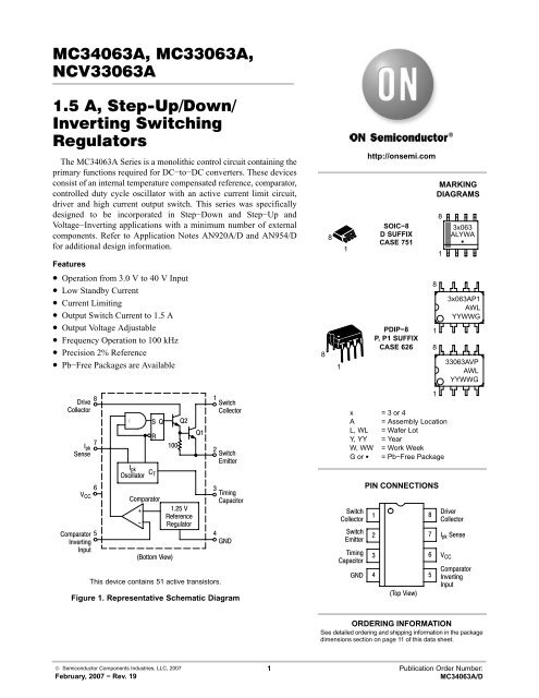
The <strong>MC34063A</strong> Series is a monolithic control circuit containing the<br />
primary functions required for DC−to−DC converters. These devices<br />
consist of an internal temperature compensated reference, comparator,<br />
controlled duty cycle oscillator with an active current limit circuit,<br />
driver and high current output switch. This series was specifically<br />
designed to be incorporated in Step−<strong>Down</strong> and <strong>Step−Up</strong> and<br />
Voltage−<strong>Inverting</strong> applications with a minimum number of external<br />
components. Refer to Application Notes AN920A/D and AN954/D<br />
for additional design information.<br />
Features<br />
• Operation from 3.0 V to 40 V Input<br />
• Low Standby Current<br />
• Current Limiting<br />
• Output Switch Current to <strong>1.5</strong> A<br />
• Output Voltage Adjustable<br />
• Frequency Operation to 100 kHz<br />
• Precision 2% Reference<br />
• Pb−Free Packages are Available<br />
8<br />
8<br />
1<br />
1<br />
http://onsemi.com<br />
SOIC−8<br />
D SUFFIX<br />
CASE 751<br />
PDIP−8<br />
P, P1 SUFFIX<br />
CASE 626<br />
8<br />
1<br />
8<br />
MARKING<br />
DIAGRAMS<br />
8<br />
1<br />
3x063<br />
ALYWA<br />
<br />
3x063AP1<br />
AWL<br />
YYWWG<br />
33063AVP<br />
AWL<br />
YYWWG<br />
Drive<br />
Collector<br />
I pk<br />
Sense<br />
8<br />
7<br />
6<br />
V CC<br />
Comparator<br />
<strong>Inverting</strong><br />
Input<br />
5<br />
I pk<br />
Oscillator<br />
S Q<br />
R<br />
C T<br />
Comparator<br />
+<br />
−<br />
100<br />
(Bottom View)<br />
Figure 1. Representative Schematic Diagram<br />
Q2<br />
1.25 V<br />
Reference<br />
Regulator<br />
Q1<br />
This device contains 51 active transistors.<br />
1<br />
2<br />
3<br />
Switch<br />
Collector<br />
Switch<br />
Emitter<br />
Timing<br />
Capacitor<br />
4<br />
GND<br />
x = 3 or 4<br />
A = Assembly Location<br />
L, WL = Wafer Lot<br />
Y, YY = Year<br />
W, WW = Work Week<br />
G or = Pb−Free Package<br />
Switch<br />
Collector<br />
Switch<br />
Emitter<br />
Timing<br />
Capacitor<br />
GND<br />
PIN CONNECTIONS<br />
1<br />
2<br />
3<br />
4 5<br />
(Top View)<br />
8<br />
7<br />
6<br />
1<br />
Driver<br />
Collector<br />
I pk Sense<br />
V CC<br />
Comparator<br />
<strong>Inverting</strong><br />
Input<br />
ORDERING INFORMATION<br />
See detailed ordering and shipping information in the package<br />
dimensions section on page 11 of this data sheet.<br />
© Semiconductor Components Industries, LLC, 2007<br />
February, 2007 − Rev. 19<br />
1 Publication Order Number:<br />
<strong>MC34063A</strong>/D
<strong>MC34063A</strong>, <strong>MC33063A</strong>, <strong>NCV33063A</strong><br />
MAXIMUM RATINGS<br />
Rating Symbol Value Unit<br />
Power Supply Voltage V CC 40 Vdc<br />
Comparator Input Voltage Range V IR −0.3 to +40 Vdc<br />
Switch Collector Voltage V C(switch) 40 Vdc<br />
Switch Emitter Voltage (V Pin 1 = 40 V) V E(switch) 40 Vdc<br />
Switch Collector to Emitter Voltage V CE(switch) 40 Vdc<br />
Driver Collector Voltage V C(driver) 40 Vdc<br />
Driver Collector Current (Note 1) I C(driver) 100 mA<br />
Switch Current I SW <strong>1.5</strong> A<br />
Power Dissipation and Thermal Characteristics<br />
Plastic Package, P, P1 Suffix<br />
T A = 25°C P D 1.25 W<br />
Thermal Resistance R JA 100 °C/W<br />
SOIC Package, D Suffix<br />
T A = 25°C P D 625 mW<br />
Thermal Resistance R JA 160 °C/W<br />
Operating Junction Temperature T J +150 °C<br />
Operating Ambient Temperature Range T A °C<br />
<strong>MC34063A</strong> 0 to +70<br />
<strong>MC33063A</strong>V, <strong>NCV33063A</strong> −40 to +125<br />
<strong>MC33063A</strong> −40 to +85<br />
Storage Temperature Range T stg −65 to +150 °C<br />
Stresses exceeding Maximum Ratings may damage the device. Maximum Ratings are stress ratings only. Functional operation above the<br />
Recommended Operating Conditions is not implied. Extended exposure to stresses above the Recommended Operating Conditions may affect<br />
device reliability.<br />
1. Maximum package power dissipation limits must be observed.<br />
2. This device series contains ESD protection and exceeds the following tests: Human Body Model 4000 V per MIL−STD−883, Method 3015.<br />
Machine Model Method 400 V.<br />
3. NCV prefix is for automotive and other applications requiring site and change control.<br />
http://onsemi.com<br />
2
<strong>MC34063A</strong>, <strong>MC33063A</strong>, <strong>NCV33063A</strong><br />
ELECTRICAL CHARACTERISTICS (V CC = 5.0 V, T A = T low to T high [Note 4], unless otherwise specified.)<br />
Characteristics Symbol Min Typ Max Unit<br />
OSCILLATOR<br />
Frequency (V Pin 5 = 0 V, C T = 1.0 nF, T A = 25°C) f osc 24 33 42 kHz<br />
Charge Current (V CC = 5.0 V to 40 V, T A = 25°C) I chg 24 35 42 A<br />
Discharge Current (V CC = 5.0 V to 40 V, T A = 25°C) I dischg 140 220 260 A<br />
Discharge to Charge Current Ratio (Pin 7 to V CC , T A = 25°C) I dischg /I chg 5.2 6.5 7.5 −<br />
Current Limit Sense Voltage (I chg = I dischg , T A = 25°C) V ipk(sense) 250 300 350 mV<br />
OUTPUT SWITCH (Note 5)<br />
Saturation Voltage, Darlington Connection<br />
(I SW = 1.0 A, Pins 1, 8 connected)<br />
Saturation Voltage (Note 6)<br />
(I SW = 1.0 A, R Pin 8 = 82 to V CC , Forced 20)<br />
V CE(sat) − 1.0 1.3 V<br />
V CE(sat) − 0.45 0.7 V<br />
DC Current Gain (I SW = 1.0 A, V CE = 5.0 V, T A = 25°C) h FE 50 75 − −<br />
Collector Off−State Current (V CE = 40 V) I C(off) − 0.01 100 A<br />
COMPARATOR<br />
Threshold Voltage<br />
T A = 25°C<br />
T A = T low to T high<br />
V th<br />
1.225<br />
1.21<br />
Threshold Voltage Line Regulation (V CC = 3.0 V to 40 V)<br />
<strong>MC33063A</strong>, <strong>MC34063A</strong><br />
<strong>MC33063A</strong>V, <strong>NCV33063A</strong><br />
Reg line<br />
Input Bias Current (V in = 0 V) I IB − −20 −400 nA<br />
TOTAL DEVICE<br />
Supply Current (V CC = 5.0 V to 40 V, C T = 1.0 nF, Pin 7 = V CC ,<br />
V Pin 5 > V th , Pin 2 = GND, remaining pins open)<br />
−<br />
−<br />
1.25<br />
−<br />
1.4<br />
1.4<br />
1.275<br />
1.29<br />
5.0<br />
6.0<br />
V<br />
mV<br />
I CC − − 4.0 mA<br />
4. T low = 0°C for <strong>MC34063A</strong>, −40°C for <strong>MC33063A</strong>, AV, <strong>NCV33063A</strong><br />
T high = +70°C for <strong>MC34063A</strong>, +85°C for <strong>MC33063A</strong>, +125°C for <strong>MC33063A</strong>V, <strong>NCV33063A</strong><br />
5. Low duty cycle pulse techniques are used during test to maintain junction temperature as close to ambient temperature as possible.<br />
6. If the output switch is driven into hard saturation (non−Darlington configuration) at low switch currents (≤ 300 mA) and high driver currents<br />
(≥ 30 mA), it may take up to 2.0 s for it to come out of saturation. This condition will shorten the off time at frequencies ≥ 30 kHz, and is<br />
magnified at high temperatures. This condition does not occur with a Darlington configuration, since the output switch cannot saturate. If a<br />
non−Darlington configuration is used, the following output drive condition is recommended:<br />
IC output<br />
Forced of output switch :<br />
I C driver – 7.0 mA * 10<br />
* The 100 resistor in the emitter of the driver device requires about 7.0 mA before the output switch conducts.<br />
http://onsemi.com<br />
3
I<br />
<strong>MC34063A</strong>, <strong>MC33063A</strong>, <strong>NCV33063A</strong><br />
, OUTPUT SWITCH ON-OFF TIME ( s)<br />
t on−off μ<br />
1000<br />
500<br />
200<br />
100<br />
50<br />
20<br />
10<br />
5.0<br />
2.0<br />
1.0<br />
V CC = 5.0 V<br />
Pin 7 = V CC<br />
Pin 5 = GND<br />
T A = 25°C<br />
0.01 0.02 0.05 0.1 0.2 0.5 1.0 2.0 5.0 10<br />
C T , OSCILLATOR TIMING CAPACITOR (nF)<br />
t on<br />
t off<br />
, OSCILLATOR VOLTAGE (V)<br />
OSC<br />
V<br />
V CC = 5.0 V<br />
Pin 7 = V CC<br />
Pin 2 = GND<br />
Pins 1, 5, 8 = Open<br />
C T = 1.0 nF<br />
T A = 25°C<br />
10 s/DIV<br />
200 mV/DIV<br />
Figure 2. Output Switch On−Off Time versus<br />
Oscillator Timing Capacitor<br />
Figure 3. Timing Capacitor Waveform<br />
, SATURATION VOLTAGE (V)<br />
CE(sat)<br />
V<br />
1.8<br />
1.7<br />
1.6<br />
<strong>1.5</strong><br />
1.4<br />
1.3<br />
V CC = 5.0 V<br />
1.2<br />
Pins 1, 7, 8 = V CC<br />
Pins 3, 5 = GND<br />
1.1<br />
T A = 25°C<br />
(See Note 7)<br />
1.0<br />
0 0.2 0.4 0.6 0.8 1.0 1.2 1.4 1.6<br />
I E , EMITTER CURRENT (A)<br />
CE(sat), SATURATION VOLTAGE (V)<br />
V<br />
1.1<br />
1.0<br />
0.9<br />
0.8<br />
0.7<br />
0.6<br />
0.5<br />
0.4<br />
0.3<br />
0.2<br />
0.1<br />
0<br />
V CC = 5.0 V<br />
Pin 7 = V CC<br />
Pins 2, 3, 5 = GND<br />
T A = 25°C<br />
(See Note 7)<br />
Darlington Connection<br />
Forced = 20<br />
0 0.2 0.4 0.6 0.8 1.0 1.2 1.4 1.6<br />
I C , COLLECTOR CURRENT(A)<br />
Figure 4. Emitter Follower Configuration Output<br />
Saturation Voltage versus Emitter Current<br />
Figure 5. Common Emitter Configuration Output<br />
Switch Saturation Voltage versus<br />
Collector Current<br />
, CURRENT LIMIT SENSE VOLTAGE (V)<br />
IPK(sense)<br />
V<br />
400<br />
380<br />
3.2<br />
V CC = 5.0 V<br />
360 I chg = I dischg<br />
2.8<br />
340<br />
2.4<br />
320<br />
2.0<br />
300<br />
280<br />
1.6<br />
260<br />
1.2<br />
C T = 1.0 nF<br />
240<br />
0.8<br />
Pin 7 = V CC<br />
Pin 2 = GND<br />
220<br />
0.4<br />
200<br />
0<br />
−55 −25 0 25 50 75 100 125<br />
0 5.0 10 15 20 25 30 35 40<br />
T A , AMBIENT TEMPERATURE (°C)<br />
V CC , SUPPLY VOLTAGE (V)<br />
CC, SUPPLY CURRENT (mA)<br />
3.6<br />
Figure 6. Current Limit Sense Voltage<br />
versus Temperature<br />
Figure 7. Standby Supply Current versus<br />
Supply Voltage<br />
7. Low duty cycle pulse techniques are used during test to maintain junction temperature as close to ambient temperature as possible.<br />
http://onsemi.com<br />
4
<strong>MC34063A</strong>, <strong>MC33063A</strong>, <strong>NCV33063A</strong><br />
170 H<br />
L<br />
8<br />
180<br />
S<br />
Q<br />
Q2<br />
1<br />
R<br />
Q1<br />
7<br />
2<br />
1N5819<br />
V in<br />
12 V<br />
R sc<br />
0.22<br />
6<br />
5<br />
V CC<br />
+<br />
−<br />
I pk<br />
OSC<br />
Comp.<br />
C T<br />
3<br />
C T<br />
1.25 V<br />
Ref<br />
Reg<br />
1500<br />
pF<br />
4<br />
R1<br />
2.2 k<br />
R2<br />
47 k<br />
+<br />
100<br />
Optional Filter<br />
1.0 H<br />
V out<br />
28 V/175 mA V out<br />
+<br />
+<br />
330 C O 100<br />
Test Conditions Results<br />
Line Regulation V in = 8.0 V to 16 V, I O = 175 mA 30 mV = ±0.05%<br />
Load Regulation V in = 12 V, I O = 75 mA to 175 mA 10 mV = ±0.017%<br />
Output Ripple V in = 12 V, I O = 175 mA 400 mVpp<br />
Efficiency V in = 12 V, I O = 175 mA 87.7%<br />
Output Ripple With Optional Filter V in = 12 V, I O = 175 mA 40 mVpp<br />
Figure 8. <strong>Step−Up</strong> Converter<br />
http://onsemi.com<br />
5
<strong>MC34063A</strong>, <strong>MC33063A</strong>, <strong>NCV33063A</strong><br />
V in<br />
8<br />
7<br />
6<br />
1<br />
2<br />
R sc<br />
1<br />
V out<br />
8<br />
V in 6<br />
7<br />
2<br />
R sc<br />
R<br />
R 0 for<br />
constant V in<br />
V out<br />
Figure 9. External Current Boost Connections for I C Peak Greater than <strong>1.5</strong> A<br />
9a. External NPN Switch 9b. External NPN Saturated Switch<br />
(See Note 8)<br />
8. If the output switch is driven into hard saturation (non−Darlington configuration) at low switch currents (≤ 300 mA) and high driver currents<br />
(≥ 30 mA), it may take up to 2.0 s to come out of saturation. This condition will shorten the off time at frequencies ≥ 30 kHz, and is magnified<br />
at high temperatures. This condition does not occur with a Darlington configuration, since the output switch cannot saturate. If a<br />
non−Darlington configuration is used, the following output drive condition is recommended.<br />
http://onsemi.com<br />
6
<strong>MC34063A</strong>, <strong>MC33063A</strong>, <strong>NCV33063A</strong><br />
8<br />
1<br />
7<br />
S<br />
R<br />
Q<br />
Q2<br />
Q1<br />
2<br />
R sc<br />
0.33<br />
V in<br />
25 V<br />
100<br />
+<br />
6<br />
5<br />
V CC<br />
+<br />
−<br />
I pk<br />
OSC<br />
Comp.<br />
C T<br />
1.25 V<br />
Ref<br />
Reg<br />
1N5819<br />
3<br />
C L T<br />
470<br />
pF<br />
4<br />
220 H<br />
R1<br />
1.2 k<br />
R2<br />
3.6 k<br />
+<br />
470 C O<br />
V out<br />
5.0 V/500 mA<br />
1.0 H<br />
V out<br />
+<br />
100<br />
Optional Filter<br />
Test Conditions Results<br />
Line Regulation V in = 15 V to 25 V, I O = 500 mA 12 mV = ±0.12%<br />
Load Regulation V in = 25 V, I O = 50 mA to 500 mA 3.0 mV = ±0.03%<br />
Output Ripple V in = 25 V, I O = 500 mA 120 mVpp<br />
Short Circuit Current V in = 25 V, R L = 0.1 1.1 A<br />
Efficiency V in = 25 V, I O = 500 mA 83.7%<br />
Output Ripple With Optional Filter V in = 25 V, I O = 500 mA 40 mVpp<br />
Figure 10. Step−<strong>Down</strong> Converter<br />
R sc<br />
V in<br />
8<br />
7<br />
6<br />
1<br />
2<br />
1<br />
8<br />
7<br />
2<br />
V out<br />
R sc<br />
V in 6<br />
V<br />
Figure 11. External Current Boost Connections for I C Peak Greater than <strong>1.5</strong> A<br />
11a. External NPN Switch 11b. External PNP Saturated Switch<br />
http://onsemi.com<br />
7
<strong>MC34063A</strong>, <strong>MC33063A</strong>, <strong>NCV33063A</strong><br />
8<br />
1<br />
S<br />
Q<br />
Q2<br />
7<br />
R<br />
Q1<br />
2<br />
V in<br />
4.5 V to 6.0 V<br />
R sc<br />
0.24<br />
6<br />
V CC<br />
I pk<br />
OSC<br />
+<br />
Comp.<br />
−<br />
C T<br />
1.25 V<br />
Ref<br />
Reg<br />
3<br />
L<br />
+<br />
88 H<br />
1500<br />
pF<br />
1N5819<br />
100 + 5<br />
4<br />
R2<br />
8.2 k<br />
R1<br />
953<br />
1000 f<br />
C O<br />
+<br />
V out<br />
−12 V/100 mA<br />
1.0 H<br />
+<br />
100<br />
V out<br />
Optional Filter<br />
Test Conditions Results<br />
Line Regulation V in = 4.5 V to 6.0 V, I O = 100 mA 3.0 mV = ± 0.012%<br />
Load Regulation V in = 5.0 V, I O = 10 mA to 100 mA 0.022 V = ± 0.09%<br />
Output Ripple V in = 5.0 V, I O = 100 mA 500 mVpp<br />
Short Circuit Current V in = 5.0 V, R L = 0.1 910 mA<br />
Efficiency V in = 5.0 V, I O = 100 mA 62.2%<br />
Output Ripple With Optional Filter V in = 5.0 V, I O = 100 mA 70 mVpp<br />
Figure 12. Voltage <strong>Inverting</strong> Converter<br />
8<br />
1<br />
V in 6<br />
3<br />
7<br />
2<br />
+<br />
1<br />
8<br />
7<br />
V<br />
2<br />
out<br />
V in 3 +<br />
6<br />
V out<br />
4<br />
4<br />
Figure 13. External Current Boost Connections for I C Peak Greater than <strong>1.5</strong> A<br />
13a. External NPN Switch 13b. External PNP Saturated Switch<br />
http://onsemi.com<br />
8
<strong>MC34063A</strong>, <strong>MC33063A</strong>, <strong>NCV33063A</strong><br />
5.45′′<br />
2.500′′<br />
(Top view, copper foil as seen through the board from the component side)<br />
<strong>MC34063A</strong> <strong>MC34063A</strong> <strong>MC34063A</strong><br />
(Top View, Component Side)<br />
*Optional Filter.<br />
Figure 14. Printed Circuit Board and Component Layout<br />
(Circuits of Figures 8, 10, 12)<br />
INDUCTOR DATA<br />
Converter Inductance (H) Turns/Wire<br />
<strong>Step−Up</strong> 170 38 Turns of #22 AWG<br />
Step−<strong>Down</strong> 220 48 Turns of #22 AWG<br />
Voltage−<strong>Inverting</strong> 88 28 Turns of #22 AWG<br />
All inductors are wound on Magnetics Inc. 55117 toroidal core.<br />
http://onsemi.com<br />
9
<strong>MC34063A</strong>, <strong>MC33063A</strong>, <strong>NCV33063A</strong><br />
Calculation <strong>Step−Up</strong> Step−<strong>Down</strong> Voltage−<strong>Inverting</strong><br />
t on /t off<br />
V out<br />
V F<br />
V in(min)<br />
V in(min)<br />
V sat<br />
V out<br />
V F<br />
V in(min)<br />
V sat<br />
V out<br />
|V out<br />
| V F<br />
V V in sat<br />
(t on + t off ) 1<br />
f<br />
1<br />
f<br />
1<br />
f<br />
t off<br />
t on t off<br />
t on t off<br />
t on t off<br />
t on<br />
t off<br />
1<br />
t on<br />
t off<br />
1<br />
t on<br />
t off<br />
1<br />
t on (t on + t off ) − t off (t on + t off ) − t off (t on + t off ) − t off<br />
C T 4.0 x 10 −5 t on 4.0 x 10 −5 t on 4.0 x 10 −5 t on<br />
I pk(switch)<br />
2I out(max)<br />
t on<br />
t off<br />
1 2I out(max) 2I out(max)<br />
t on<br />
t off<br />
1<br />
R sc 0.3/I pk(switch) 0.3/I pk(switch) 0.3/I pk(switch)<br />
L (min)<br />
(V in(min) V sat )<br />
I pk(switch)<br />
t on(max)<br />
(V in(min) V sat V out )<br />
I pk(switch)<br />
t on(max)<br />
(V in(min) V sat )<br />
I pk(switch)<br />
t on(max)<br />
C O<br />
9<br />
I out<br />
t on<br />
I pk(switch)<br />
(t on t off<br />
)<br />
9<br />
V ripple(pp) 8V ripple(pp)<br />
I out<br />
t on<br />
V ripple(pp)<br />
V sat = Saturation voltage of the output switch.<br />
V F = Forward voltage drop of the output rectifier.<br />
The following power supply characteristics must be chosen:<br />
V in − Nominal input voltage.<br />
V out − Desired output voltage,<br />
I out − Desired output current.<br />
|V out | 1.25 1 R2<br />
R1 <br />
f min − Minimum desired output switching frequency at the selected values of V in and I O .<br />
V ripple(pp) − Desired peak−to−peak output ripple voltage. In practice, the calculated capacitor value will need to be increased due to its<br />
equivalent series resistance and board layout. The ripple voltage should be kept to a low value since it will directly affect the<br />
line and load regulation.<br />
NOTE: For further information refer to Application Note AN920A/D and AN954/D.<br />
Figure 15. Design Formula Table<br />
http://onsemi.com<br />
10
<strong>MC34063A</strong>, <strong>MC33063A</strong>, <strong>NCV33063A</strong><br />
ORDERING INFORMATION<br />
Device Package Shipping †<br />
<strong>MC33063A</strong>D SOIC−8 98 Units / Rail<br />
<strong>MC33063A</strong>DG<br />
SOIC−8<br />
(Pb−Free)<br />
98 Units / Rail<br />
<strong>MC33063A</strong>DR2 SOIC−8 2500 Units / Tape & Reel<br />
<strong>MC33063A</strong>DR2G<br />
SOIC−8<br />
(Pb−Free)<br />
2500 Units / Tape & Reel<br />
<strong>MC33063A</strong>P1 PDIP−8 50 Units / Rail<br />
<strong>MC33063A</strong>P1G<br />
PDIP−8<br />
(Pb−Free)<br />
50 Units / Rail<br />
<strong>MC33063A</strong>VD SOIC−8 98 Units / Rail<br />
<strong>MC33063A</strong>VDG<br />
SOIC−8<br />
(Pb−Free)<br />
98 Units / Rail<br />
<strong>MC33063A</strong>VDR2<br />
<strong>MC33063A</strong>VDR2G<br />
<strong>NCV33063A</strong>VDR2*<br />
<strong>NCV33063A</strong>VDR2G*<br />
SOIC−8<br />
SOIC−8<br />
(Pb−Free)<br />
SOIC−8<br />
SOIC−8<br />
(Pb−Free)<br />
2500 Units / Tape & Reel<br />
<strong>MC33063A</strong>VP PDIP−8 50 Units / Rail<br />
<strong>MC33063A</strong>VPG<br />
PDIP−8<br />
(Pb−Free)<br />
50 Units / Rail<br />
<strong>MC34063A</strong>D SOIC−8 98 Units / Rail<br />
<strong>MC34063A</strong>DG<br />
SOIC−8<br />
(Pb−Free)<br />
98 Units / Rail<br />
<strong>MC34063A</strong>DR2 SOIC−8 2500 Units / Tape & Reel<br />
<strong>MC34063A</strong>DR2G<br />
SOIC−8<br />
(Pb−Free)<br />
2500 Units / Tape & Reel<br />
<strong>MC34063A</strong>P1 PDIP−8 50 Units / Rail<br />
<strong>MC34063A</strong>P1G<br />
PDIP−8<br />
(Pb−Free)<br />
50 Units / Rail<br />
†For information on tape and reel specifications, including part orientation and tape sizes, please refer to our Tape and Reel Packaging<br />
Specification Brochure, BRD8011/D.<br />
*<strong>NCV33063A</strong>: T low = −40°C, T high = +125°C. Guaranteed by design. NCV prefix is for automotive and other applications requiring site and<br />
change control.<br />
http://onsemi.com<br />
11
<strong>MC34063A</strong>, <strong>MC33063A</strong>, <strong>NCV33063A</strong><br />
PACKAGE DIMENSIONS<br />
SOIC−8 NB<br />
D SUFFIX<br />
CASE 751−07<br />
ISSUE AG<br />
−X−<br />
B<br />
−Y−<br />
−Z−<br />
H<br />
8<br />
1<br />
G<br />
A<br />
D<br />
5<br />
4<br />
S<br />
C<br />
0.25 (0.010) M Z Y S X S<br />
0.25 (0.010) M<br />
SEATING<br />
PLANE<br />
Y<br />
0.10 (0.004)<br />
M<br />
N X 45<br />
M<br />
K<br />
J<br />
NOTES:<br />
1. DIMENSIONING AND TOLERANCING PER<br />
ANSI Y14.5M, 1982.<br />
2. CONTROLLING DIMENSION: MILLIMETER.<br />
3. DIMENSION A AND B DO NOT INCLUDE<br />
MOLD PROTRUSION.<br />
4. MAXIMUM MOLD PROTRUSION 0.15 (0.006)<br />
PER SIDE.<br />
5. DIMENSION D DOES NOT INCLUDE DAMBAR<br />
PROTRUSION. ALLOWABLE DAMBAR<br />
PROTRUSION SHALL BE 0.127 (0.005) TOTAL<br />
IN EXCESS OF THE D DIMENSION AT<br />
MAXIMUM MATERIAL CONDITION.<br />
6. 751−01 THRU 751−06 ARE OBSOLETE. NEW<br />
STANDARD IS 751−07.<br />
MILLIMETERS INCHES<br />
DIM MIN MAX MIN MAX<br />
A 4.80 5.00 0.189 0.197<br />
B 3.80 4.00 0.150 0.157<br />
C 1.35 1.75 0.053 0.069<br />
D 0.33 0.51 0.013 0.020<br />
G 1.27 BSC 0.050 BSC<br />
H 0.10 0.25 0.004 0.010<br />
J 0.19 0.25 0.007 0.010<br />
K 0.40 1.27 0.016 0.050<br />
M 0 8 0 8 <br />
N 0.25 0.50 0.010 0.020<br />
S 5.80 6.20 0.228 0.244<br />
SOLDERING FOOTPRINT*<br />
<strong>1.5</strong>2<br />
0.060<br />
7.0<br />
0.275<br />
4.0<br />
0.155<br />
0.6<br />
0.024<br />
1.270<br />
0.050<br />
SCALE 6:1<br />
mm<br />
inches <br />
*For additional information on our Pb−Free strategy and soldering<br />
details, please download the ON Semiconductor Soldering and<br />
Mounting Techniques Reference Manual, SOLDERRM/D.<br />
http://onsemi.com<br />
12
<strong>MC34063A</strong>, <strong>MC33063A</strong>, <strong>NCV33063A</strong><br />
PACKAGE DIMENSIONS<br />
PDIP−8<br />
P, P1 SUFFIX<br />
CASE 626−05<br />
ISSUE L<br />
8<br />
5<br />
−B−<br />
NOTES:<br />
1. DIMENSION L TO CENTER OF LEAD WHEN<br />
FORMED PARALLEL.<br />
2. PACKAGE CONTOUR OPTIONAL (ROUND OR<br />
SQUARE CORNERS).<br />
3. DIMENSIONING AND TOLERANCING PER ANSI<br />
Y14.5M, 1982.<br />
NOTE 2<br />
−T−<br />
SEATING<br />
PLANE<br />
H<br />
1 4<br />
F<br />
−A−<br />
C<br />
N<br />
D K<br />
G<br />
0.13 (0.005) M T A M B M<br />
L<br />
J<br />
M<br />
MILLIMETERS INCHES<br />
DIM MIN MAX MIN MAX<br />
A 9.40 10.16 0.370 0.400<br />
B 6.10 6.60 0.240 0.260<br />
C 3.94 4.45 0.155 0.175<br />
D 0.38 0.51 0.015 0.020<br />
F 1.02 1.78 0.040 0.070<br />
G 2.54 BSC 0.100 BSC<br />
H 0.76 1.27 0.030 0.050<br />
J 0.20 0.30 0.008 0.012<br />
K 2.92 3.43 0.115 0.135<br />
L 7.62 BSC 0.300 BSC<br />
M −−− 10 −−− 10 <br />
N 0.76 1.01 0.030 0.040<br />
SENSEFET is a trademark of Semiconductor Components Industries, LLC.<br />
ON Semiconductor and are registered trademarks of Semiconductor Components Industries, LLC (SCILLC). SCILLC reserves the right to make changes without further notice<br />
to any products herein. SCILLC makes no warranty, representation or guarantee regarding the suitability of its products for any particular purpose, nor does SCILLC assume any liability<br />
arising out of the application or use of any product or circuit, and specifically disclaims any and all liability, including without limitation special, consequential or incidental damages.<br />
“Typical” parameters which may be provided in SCILLC data sheets and/or specifications can and do vary in different applications and actual performance may vary over time. All<br />
operating parameters, including “Typicals” must be validated for each customer application by customer’s technical experts. SCILLC does not convey any license under its patent rights<br />
nor the rights of others. SCILLC products are not designed, intended, or authorized for use as components in systems intended for surgical implant into the body, or other applications<br />
intended to support or sustain life, or for any other application in which the failure of the SCILLC product could create a situation where personal injury or death may occur. Should<br />
Buyer purchase or use SCILLC products for any such unintended or unauthorized application, Buyer shall indemnify and hold SCILLC and its officers, employees, subsidiaries, affiliates,<br />
and distributors harmless against all claims, costs, damages, and expenses, and reasonable attorney fees arising out of, directly or indirectly, any claim of personal injury or death<br />
associated with such unintended or unauthorized use, even if such claim alleges that SCILLC was negligent regarding the design or manufacture of the part. SCILLC is an Equal<br />
Opportunity/Affirmative Action Employer. This literature is subject to all applicable copyright laws and is not for resale in any manner.<br />
PUBLICATION ORDERING INFORMATION<br />
LITERATURE FULFILLMENT:<br />
Literature Distribution Center for ON Semiconductor<br />
P.O. Box 5163, Denver, Colorado 80217 USA<br />
Phone: 303−675−2175 or 800−344−3860 Toll Free USA/Canada<br />
Fax: 303−675−2176 or 800−344−3867 Toll Free USA/Canada<br />
Email: orderlit@onsemi.com<br />
N. American Technical Support: 800−282−9855 Toll Free<br />
USA/Canada<br />
Europe, Middle East and Africa Technical Support:<br />
Phone: 421 33 790 2910<br />
Japan Customer Focus Center<br />
Phone: 81−3−5773−3850<br />
http://onsemi.com<br />
13<br />
ON Semiconductor Website: www.onsemi.com<br />
Order Literature: http://www.onsemi.com/orderlit<br />
For additional information, please contact your local<br />
Sales Representative<br />
<strong>MC34063A</strong>/D